

Comparative Study: Chiplet Integration vs Traditional Semiconductor Design
OCT 15, 20259 MIN READ
Generate Your Research Report Instantly with AI Agent
PatSnap Eureka helps you evaluate technical feasibility & market potential.
Chiplet Technology Evolution and Objectives
The semiconductor industry has witnessed a remarkable evolution over the past six decades, following Moore's Law which predicted the doubling of transistor density approximately every two years. Traditional monolithic integrated circuit design has been the cornerstone of this progress, with manufacturers continuously shrinking transistor sizes to pack more functionality onto a single silicon die. However, as we approach physical limits at sub-7nm nodes, this approach faces mounting challenges including increased manufacturing complexity, rising costs, and diminishing returns on performance improvements.
Chiplet technology emerged as a revolutionary approach to address these limitations. Rather than fabricating an entire system on a single die, chiplet architecture disaggregates complex systems into smaller functional blocks (chiplets) that are manufactured separately and then integrated using advanced packaging technologies. This paradigm shift began gaining significant traction around 2015-2017, with AMD's introduction of their Infinity Fabric interconnect and subsequent Ryzen processors based on chiplet design.
The evolution of chiplet technology can be traced through several key developments. Initially, multi-chip modules (MCMs) in the 1980s and 1990s represented early attempts at component integration. The true chiplet revolution accelerated with the development of advanced packaging technologies such as 2.5D integration with silicon interposers, followed by more sophisticated approaches including Embedded Multi-die Interconnect Bridge (EMIB) by Intel and Integrated Fan-Out (InFO) by TSMC.
Interconnect technologies have evolved in parallel, progressing from traditional wire bonding to through-silicon vias (TSVs), and now to advanced die-to-die interfaces that support high-bandwidth, low-latency communication between chiplets. Standards like Universal Chiplet Interconnect Express (UCIe) are emerging to establish industry-wide protocols for chiplet integration.
The primary objectives of chiplet technology are multifaceted. First, it aims to overcome the economic barriers of advanced node manufacturing by allowing companies to mix-and-match process nodes, using cutting-edge processes only where necessary while implementing less critical functions on mature, cost-effective nodes. Second, it enables greater design flexibility and reusability, with standardized chiplets potentially serving as building blocks across multiple products. Third, it addresses yield challenges by reducing the effective die size of individual components, thereby improving manufacturing yields and reducing costs.
Looking forward, chiplet technology seeks to enable heterogeneous integration, combining different types of semiconductors (logic, memory, analog, RF) that traditionally couldn't be optimized on a single process. This "More than Moore" approach promises to deliver continued performance scaling even as traditional dimensional scaling slows, positioning chiplet integration as a cornerstone of semiconductor advancement for the coming decades.
Market Demand Analysis for Chiplet Integration
The global semiconductor market is experiencing a significant shift towards chiplet integration technology, driven by increasing demand for more powerful computing solutions while facing the physical limitations of traditional monolithic designs. Market research indicates that the chiplet market is projected to grow at a compound annual growth rate of over 40% from 2023 to 2030, reaching tens of billions of dollars by the end of the decade. This remarkable growth trajectory reflects the urgent industry need for more efficient semiconductor design approaches.
The primary market demand for chiplet integration stems from high-performance computing sectors, including data centers, artificial intelligence applications, and cloud service providers. These segments require exponentially increasing computational power while maintaining energy efficiency. Traditional monolithic designs have reached scaling limitations, creating a performance gap that chiplet technology effectively addresses.
Enterprise customers represent the largest market segment currently adopting chiplet technology, particularly in server and data center applications where performance and power efficiency directly impact operational costs. The hyperscale cloud providers have become early adopters, implementing chiplet-based processors to handle massive computational workloads while reducing energy consumption.
Consumer electronics manufacturers are also showing increasing interest in chiplet technology, particularly for premium devices where performance differentiation provides competitive advantage. Mobile device manufacturers are exploring chiplet designs to deliver enhanced AI capabilities while maintaining battery life. The gaming industry similarly seeks chiplet solutions to deliver console-level performance in portable form factors.
Automotive and industrial sectors represent emerging markets for chiplet technology, driven by the growing computational requirements of autonomous driving systems, advanced driver assistance features, and industrial automation. These applications demand both high performance and reliability in challenging environmental conditions, which modular chiplet designs can potentially address more effectively than traditional approaches.
From a geographical perspective, North America and East Asia dominate the chiplet market demand, with major technology companies and semiconductor manufacturers investing heavily in research and development. Europe is also accelerating investments in chiplet technology as part of broader semiconductor sovereignty initiatives.
The market demand is further characterized by increasing emphasis on customization capabilities. Enterprise customers seek semiconductor solutions tailored to specific workloads, which chiplet technology enables through mix-and-match integration of specialized processing elements. This customization potential represents a significant shift from the more standardized offerings of traditional semiconductor designs.
Current State and Challenges in Chiplet Technology
Chiplet technology has emerged as a revolutionary approach in semiconductor design, offering a modular alternative to traditional monolithic integration. Currently, chiplet implementation has gained significant traction among major semiconductor manufacturers including AMD, Intel, and TSMC. The technology allows for the disaggregation of system-on-chip (SoC) designs into smaller functional blocks that can be manufactured separately and then integrated using advanced packaging technologies.
The global chiplet market is experiencing rapid growth, with projections indicating a compound annual growth rate exceeding 40% through 2027. This acceleration is primarily driven by the increasing complexity of semiconductor designs and the economic challenges associated with scaling monolithic chips to advanced process nodes. Industry adoption has been particularly strong in high-performance computing, data centers, and AI applications where performance and efficiency demands are most stringent.
Despite its promising trajectory, chiplet technology faces several significant technical challenges. The most pressing issue involves die-to-die interconnects, where achieving sufficient bandwidth, low latency, and power efficiency remains difficult. Current solutions like Intel's EMIB, TSMC's CoWoS, and AMD's Infinity Fabric each present different trade-offs between performance, manufacturing complexity, and cost.
Thermal management presents another substantial hurdle, as the integration of multiple dies in close proximity creates hotspots and thermal gradients that can affect reliability and performance. The industry has yet to standardize effective cooling solutions for complex chiplet designs, particularly in high-density applications.
Testing and yield management constitute additional challenges. Unlike traditional monolithic designs, chiplet-based systems require testing at multiple levels: individual chiplets, interconnects, and the integrated package. This multi-level testing complexity increases manufacturing costs and time-to-market. Known-good-die testing methodologies are still evolving to address these challenges effectively.
The lack of standardization across the industry represents perhaps the most significant barrier to widespread adoption. While initiatives like the Universal Chiplet Interconnect Express (UCIe) consortium are making progress, the ecosystem remains fragmented with proprietary interfaces and packaging technologies dominating the landscape. This fragmentation limits interoperability between chiplets from different vendors and increases design complexity.
From a geographical perspective, chiplet technology development is concentrated in several key regions. North America leads in architectural innovation through companies like AMD and Intel, while East Asia, particularly Taiwan and South Korea, dominates in manufacturing and packaging technologies. Europe has established expertise in specific applications, especially automotive and industrial chiplet implementations, though at a smaller scale than its global counterparts.
Technical Approaches to Chiplet Integration
01 Advanced Chiplet Integration Architectures
Modern semiconductor design has evolved to incorporate chiplet-based architectures that allow for more efficient integration of multiple functional blocks. These architectures enable designers to combine different chiplets manufactured using optimal process technologies, resulting in improved performance, reduced power consumption, and enhanced scalability. The integration techniques include advanced packaging technologies, interposer-based connections, and specialized interconnect fabrics that facilitate high-bandwidth, low-latency communication between chiplets.- Chiplet architecture for improved integration efficiency: Chiplet architecture enables more efficient integration of semiconductor components by allowing different functional blocks to be manufactured separately and then combined into a single package. This approach improves yield, reduces costs, and allows for mixing of process technologies. The architecture facilitates better thermal management and power distribution across the integrated system, resulting in higher performance and energy efficiency compared to traditional monolithic designs.
- Advanced interconnect technologies for chiplet integration: Novel interconnect technologies are essential for efficient chiplet integration, enabling high-bandwidth, low-latency communication between chiplets. These technologies include advanced packaging methods, through-silicon vias (TSVs), silicon interposers, and micro-bumps. The interconnect solutions address challenges in signal integrity, power delivery, and thermal management while maintaining high data transfer rates between integrated components, which is critical for overall system performance.
- Design automation tools for chiplet-based systems: Specialized electronic design automation (EDA) tools have been developed to address the unique challenges of chiplet-based system design. These tools facilitate the integration process by providing capabilities for multi-die floorplanning, inter-chiplet communication optimization, and system-level verification. They enable designers to efficiently manage the complexity of chiplet-based designs, optimize performance, and reduce time-to-market compared to traditional monolithic design approaches.
- Heterogeneous integration of diverse technologies: Heterogeneous integration enables the combination of diverse semiconductor technologies (analog, digital, RF, memory) in a single package using chiplets. This approach allows each component to be manufactured using its optimal process technology, overcoming the limitations of traditional monolithic integration. The resulting systems benefit from improved performance, reduced power consumption, and enhanced functionality while maintaining cost efficiency through optimized manufacturing processes for each component.
- Testing and yield management strategies for chiplet systems: Specialized testing and yield management strategies have been developed for chiplet-based systems to ensure reliability and performance. These include known-good-die testing before integration, built-in self-test mechanisms, and redundancy schemes. The approaches enable more efficient identification and isolation of defects compared to traditional monolithic designs, resulting in higher overall yield and reduced manufacturing costs while maintaining system reliability and performance standards.
02 Interconnect Technologies for Chiplet Integration
Specialized interconnect technologies are crucial for efficient chiplet integration. These include advanced die-to-die interfaces, through-silicon vias (TSVs), silicon interposers, and organic substrates that enable high-speed communication between chiplets. The interconnect solutions address challenges related to signal integrity, power delivery, thermal management, and mechanical stability, while supporting the increasing bandwidth requirements of modern semiconductor designs.Expand Specific Solutions03 Design Methodologies and Tools for Chiplet-based Systems
Specialized design methodologies and EDA tools have been developed to address the unique challenges of chiplet-based system design. These include partitioning strategies, floorplanning techniques, and verification methodologies that account for the distributed nature of chiplet architectures. The tools enable designers to optimize the overall system performance while managing the complexity of integrating multiple chiplets with different characteristics and requirements.Expand Specific Solutions04 Manufacturing and Testing Approaches for Chiplet Integration
Novel manufacturing and testing approaches have been developed to ensure the reliability and yield of chiplet-based systems. These include advanced packaging techniques, known-good-die testing methodologies, and post-integration validation strategies. The approaches address challenges related to thermal management, mechanical stress, and electrical performance verification in multi-chiplet systems, ensuring that the integrated solution meets the required specifications and reliability targets.Expand Specific Solutions05 Comparison of Chiplet Integration with Traditional Monolithic Designs
Comparative analyses between chiplet-based integration and traditional monolithic designs highlight the efficiency advantages of the chiplet approach. These include improved yield, cost-effectiveness for large designs, ability to mix process technologies, and enhanced design reuse. The analyses also address the challenges and overhead associated with chiplet integration, such as increased packaging complexity, potential performance penalties from inter-chiplet communication, and design partitioning considerations.Expand Specific Solutions
Key Industry Players in Chiplet Ecosystem
The chiplet integration market is currently in a growth phase, with increasing adoption as an alternative to traditional monolithic semiconductor designs. The market is expanding rapidly, driven by demand for higher performance, lower costs, and improved yields in advanced nodes. Major semiconductor manufacturers including TSMC, Intel, AMD, and Samsung Electronics are heavily investing in chiplet technology, with AMD leading commercial implementation through its Zen architecture. Intel is advancing with its EMIB and Foveros technologies, while TSMC offers advanced packaging solutions like CoWoS and InFO. The technology maturity varies across players, with established semiconductor manufacturers further along the adoption curve compared to newer entrants. This fragmented competitive landscape includes both IDMs and foundries competing to establish dominant interconnect standards and packaging technologies.
Taiwan Semiconductor Manufacturing Co., Ltd.
Technical Solution: TSMC has developed advanced chiplet integration technologies through its 3DFabric platform, which includes TSMC-SoIC (System on Integrated Chips), InFO (Integrated Fan-Out), and CoWoS (Chip on Wafer on Substrate). SoIC enables true 3D stacking with micron-level bonding pitches and up to 10,000 interconnections per mm², achieving near-monolithic performance. Their CoWoS technology provides high-bandwidth, low-latency connections between chiplets on a silicon interposer, supporting HBM memory integration and used in high-performance computing applications. TSMC's InFO technology offers a cost-effective packaging solution for mobile and edge applications, with reduced form factors and improved thermal performance. Their latest advancements include hybrid bonding techniques that achieve sub-10 micron interconnect pitches, enabling bandwidth exceeding 4 TB/s between chiplets while maintaining energy efficiency below 0.3 pJ/bit.
Strengths: Industry-leading process technology enables highest transistor density; extensive ecosystem partnerships provide comprehensive design solutions; proven high-volume manufacturing capability; superior interconnect density and energy efficiency metrics. Weaknesses: Higher manufacturing costs compared to traditional designs; requires specialized design and testing methodologies; thermal challenges in densely packed chiplet arrangements; intellectual property coordination challenges with multiple chiplet vendors.
Intel Corp.
Technical Solution: Intel has pioneered chiplet integration through its EMIB (Embedded Multi-die Interconnect Bridge) and Foveros 3D packaging technologies. EMIB enables high-density connections between chiplets in a planar arrangement using silicon bridges embedded in the package substrate, while Foveros allows for vertical stacking of compute tiles. Intel's Ponte Vecchio GPU utilizes both technologies, incorporating over 47 tiles manufactured on different process nodes. Their Meteor Lake processors feature a disaggregated design with separate compute, graphics, I/O, and SoC tiles. Intel's approach allows mixing of process nodes and IP blocks, with interconnects achieving up to 2 TB/s bandwidth between chiplets. Their Co-EMIB technology combines EMIB and Foveros for complex multi-chiplet designs, enabling a "system-in-package" approach rather than traditional monolithic SoCs.
Strengths: Flexibility to mix process nodes for cost optimization; reduced die size improves yield rates; faster time-to-market through parallel development of chiplets; ability to combine different IP blocks efficiently. Weaknesses: Increased packaging complexity and costs; potential performance overhead from inter-chiplet communication; thermal management challenges in dense chiplet arrangements; requires sophisticated design tools and expertise.
Core Innovations in Die-to-Die Interconnects
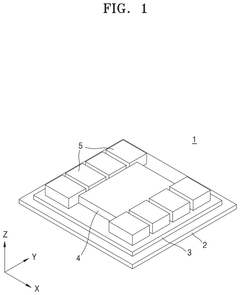
Semiconductor device
PatentPendingUS20250293165A1
Innovation
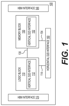
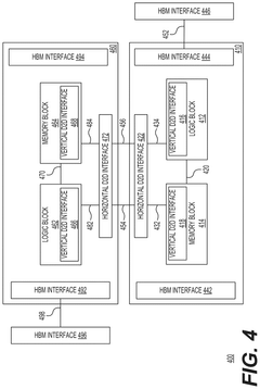
- A semiconductor device with configurable chiplet dies and an interposer, featuring a die-to-die interface with adjustable modules and a selection circuit that allows for variable alignment of connection modules, enabling efficient inter-chiplet communication without the need for new chiplet designs.
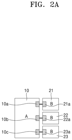
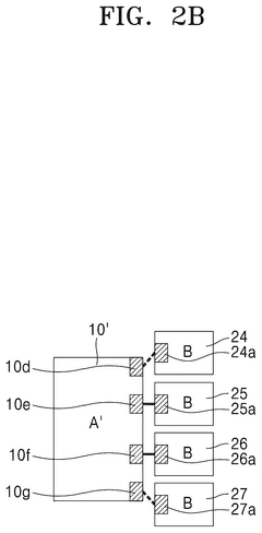
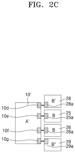
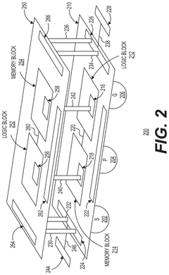
Homogeneous chiplets configurable as a two-dimensional system or a three-dimensional system
PatentPendingUS20250038120A1
Innovation
- A homogeneous chiplet system is introduced, comprising vertically stacked or horizontally coupled chiplets with on-die interconnect structures and vertical die-to-die interconnection structures, allowing for efficient data signal transfer and reducing latency.
Cost-Performance Trade-offs Analysis
The economic implications of chiplet integration versus traditional monolithic design represent a critical decision point for semiconductor manufacturers. Initial capital expenditure for chiplet-based designs typically exceeds that of traditional approaches by 15-25%, primarily due to the need for specialized packaging equipment, advanced interconnect technologies, and more complex testing infrastructure. However, this investment often yields significant long-term cost advantages through improved yield rates.
Yield considerations heavily favor chiplet architectures, particularly at advanced nodes below 7nm. Statistical analysis demonstrates that dividing a 600mm² monolithic die into four 150mm² chiplets can improve final product yield from approximately 70% to over 90%, translating to a 20-30% reduction in per-unit production costs at scale. This yield advantage becomes more pronounced as process nodes shrink, making chiplet designs increasingly economical for cutting-edge applications.
Time-to-market metrics reveal another dimension of the cost-performance equation. Traditional monolithic designs typically require 18-24 months from conception to production, while chiplet-based approaches can reduce this cycle to 12-18 months through parallel development of individual components. This acceleration can provide significant competitive advantages in rapidly evolving markets such as AI accelerators and high-performance computing.
Performance trade-offs must be carefully evaluated against these economic benefits. Inter-chiplet communication introduces latency penalties of 5-15 nanoseconds compared to on-die communication, potentially impacting applications with extreme latency sensitivity. Power consumption increases by 5-10% due to additional I/O requirements for inter-chiplet communication, though this can be partially mitigated through advanced packaging technologies like EMIB or CoWoS.
The economic calculus shifts dramatically based on production volume. For high-volume consumer products exceeding 10 million units annually, the amortized tooling costs and yield benefits of chiplet designs typically deliver 15-25% cost advantages. Conversely, for specialized products with annual volumes below 100,000 units, traditional monolithic approaches often remain more cost-effective despite lower yields, as they avoid the fixed costs associated with complex integration technologies.
Manufacturing flexibility represents an often-overlooked economic advantage of chiplet architectures. The ability to mix process nodes allows companies to optimize cost-performance ratios by implementing only performance-critical components at advanced nodes while utilizing mature, cost-effective nodes for peripheral functions. This selective application of advanced fabrication can reduce overall silicon costs by 20-40% compared to all-advanced-node monolithic implementations.
Standardization Efforts in Chiplet Interfaces
The standardization of chiplet interfaces represents a critical frontier in the evolution of semiconductor design methodologies. As chiplet integration gains momentum across the industry, the lack of universal interface standards has emerged as a significant barrier to widespread adoption. Several industry consortia and leading semiconductor companies have recognized this challenge and initiated collaborative efforts to establish common frameworks for chiplet interconnection.
The Universal Chiplet Interconnect Express (UCIe) consortium, formed in 2022, stands as one of the most prominent standardization initiatives. Founding members including Intel, AMD, Arm, TSMC, and Samsung have collectively developed specifications for die-to-die interconnects that address physical layer, protocol stack, and software considerations. UCIe aims to create an open ecosystem where chiplets from different vendors can seamlessly integrate, fostering innovation while reducing development costs.
Parallel to UCIe, the Open Compute Project (OCP) has advanced the Open Domain-Specific Architecture (ODSA) subproject, which focuses on establishing chiplet design and integration standards. The ODSA has made significant progress in defining physical and logical interfaces through its Bunch of Wires (BoW) specification, which offers a straightforward approach to chiplet connectivity with scalable bandwidth options.
JEDEC, a long-established standards organization in the semiconductor industry, has also entered the chiplet standardization arena with its JC-70 committee working on memory-centric chiplet interfaces. Their efforts complement existing standards by addressing the specific requirements of memory integration in heterogeneous systems.
The Advanced Interface Bus (AIB) developed by Intel represents another important contribution to chiplet interface standardization. While initially proprietary, Intel has made AIB available through open licensing, allowing broader industry adoption. AIB offers high-bandwidth, low-latency connections crucial for high-performance computing applications.
These standardization initiatives face several technical challenges, including signal integrity across different process nodes, power management across chiplet boundaries, and thermal considerations in densely packed multi-chiplet designs. Testing methodologies for multi-vendor chiplet systems present additional complexities that standards must address.
The economic implications of successful chiplet interface standardization are substantial. Industry analysts project that standardized interfaces could reduce design costs by up to 30% while accelerating time-to-market by enabling pre-validated chiplet libraries. Furthermore, standardization may democratize semiconductor innovation by lowering barriers to entry for smaller design houses that can focus on specialized chiplets rather than complete SoC designs.
Unlock deeper insights with PatSnap Eureka Quick Research — get a full tech report to explore trends and direct your research. Try now!
Generate Your Research Report Instantly with AI Agent
Supercharge your innovation with PatSnap Eureka AI Agent Platform!