

Comparing Industry Standards for Chiplet Integration Solutions
OCT 15, 20259 MIN READ
Generate Your Research Report Instantly with AI Agent
PatSnap Eureka helps you evaluate technical feasibility & market potential.
Chiplet Integration Standards Evolution and Objectives
The evolution of chiplet integration technology represents a paradigm shift in semiconductor design and manufacturing, moving from traditional monolithic System-on-Chip (SoC) approaches toward more modular and flexible architectures. This transition began in the early 2010s when semiconductor scaling challenges became increasingly apparent, with Moore's Law facing physical and economic limitations. The industry recognized that disaggregating complex systems into smaller, specialized dies (chiplets) could provide a viable path forward for continued performance improvements and cost optimization.
The initial chiplet implementations were proprietary solutions developed by companies like AMD, with their Infinity Fabric interconnect introduced in 2017, and Intel's Embedded Multi-die Interconnect Bridge (EMIB) technology. These early approaches demonstrated the feasibility of chiplet-based designs but highlighted the need for standardization to enable broader ecosystem adoption and interoperability.
By 2019-2020, industry consortia began forming to address standardization challenges, with the Open Compute Project (OCP) and DARPA's Common Heterogeneous Integration and IP Reuse Strategies (CHIPS) program playing pivotal roles. These initiatives aimed to establish common interfaces, protocols, and design methodologies for chiplet integration across different vendors and technology nodes.
The primary objectives of chiplet integration standards development include enabling a more diverse and competitive semiconductor ecosystem, reducing design and manufacturing costs, accelerating time-to-market for complex systems, and extending the benefits of semiconductor scaling beyond traditional approaches. Standards seek to define physical interfaces, logical protocols, power management schemes, testing methodologies, and design tools that facilitate seamless integration of chiplets from different vendors.
Current standardization efforts focus on several key areas: die-to-die interfaces (both physical and logical), packaging technologies, thermal management, power delivery, signal integrity, and testing methodologies. Major standards initiatives include the Universal Chiplet Interconnect Express (UCIe), Advanced Interface Bus (AIB), Bunch of Wires (BoW), and Open Domain-Specific Architecture (ODSA).
The technology trajectory suggests continued evolution toward more sophisticated integration standards that will eventually enable a true "chiplet marketplace" where system designers can select pre-validated chiplets from various vendors and integrate them with minimal custom engineering. This vision requires not only technical standards but also business models and supply chain frameworks that support chiplet-based design and manufacturing.
Looking forward, chiplet integration standards will likely expand to address emerging requirements such as optical interconnects, advanced packaging technologies like 3D stacking, and specialized interfaces for domain-specific applications including AI accelerators, high-performance computing, and edge devices.
Market Demand Analysis for Chiplet Technology
The chiplet integration market is experiencing unprecedented growth driven by the semiconductor industry's shift away from traditional monolithic designs. As Moore's Law faces physical and economic limitations, chiplet technology has emerged as a strategic solution to continue performance scaling while managing costs. Current market analysis indicates the global chiplet market is projected to reach $57 billion by 2035, with a compound annual growth rate exceeding 40% from 2023 to 2030.
Primary demand drivers include high-performance computing, data centers, and AI applications where computational requirements are growing exponentially. These sectors require solutions that balance performance, power efficiency, and cost-effectiveness—precisely what chiplet architecture offers. Cloud service providers and hyperscalers are particularly aggressive in adopting chiplet-based solutions to address their massive computational needs while optimizing their total cost of ownership.
The automotive and edge computing sectors represent rapidly expanding market segments for chiplet technology. Advanced driver-assistance systems and autonomous driving capabilities demand increasingly sophisticated processing capabilities that can be efficiently delivered through heterogeneous integration. Similarly, IoT applications benefit from chiplet designs that combine various functional blocks optimized for specific tasks.
Market research indicates strong regional variations in chiplet adoption. North America leads in terms of market share, driven by major technology companies and cloud service providers. Asia-Pacific represents the fastest-growing region, supported by substantial investments in semiconductor manufacturing infrastructure and government initiatives promoting technological self-sufficiency.
Customer requirements analysis reveals several critical market demands. First, standardization of interfaces between chiplets from different vendors ranks as the top priority, with 78% of potential adopters citing interoperability as their primary concern. Second, thermal management solutions for densely packed chiplet designs represent a significant market need. Third, testing methodologies specific to multi-die packages are increasingly demanded as companies transition to chiplet architectures.
The market is also witnessing a shift in supply chain dynamics. Traditional integrated device manufacturers are adapting their business models to accommodate chiplet-based designs, while fabless companies are exploring new partnership opportunities. This evolution is creating demand for specialized packaging services and design tools specifically tailored for chiplet integration.
Economic analysis demonstrates compelling cost advantages driving market demand. For advanced nodes below 5nm, chiplet-based designs can reduce development costs by up to 25% compared to monolithic approaches while improving yields and time-to-market. These economic benefits are accelerating adoption across multiple industry segments.
Current Landscape and Technical Challenges in Chiplet Integration
The chiplet integration landscape has evolved significantly over the past decade, transitioning from traditional monolithic system-on-chip (SoC) designs to more modular approaches. Currently, several industry standards are competing for dominance in this rapidly developing field, each with distinct technical foundations and ecosystem support. The Universal Chiplet Interconnect Express (UCIe) has emerged as a prominent standard, backed by industry giants including Intel, AMD, Arm, and TSMC, focusing on die-to-die interconnects with standardized physical and protocol layers.
Concurrently, JEDEC's Chiplet Multi-Die Interconnect (CMI) standard addresses memory-centric integration challenges, while the Open Compute Project's Bunch of Wires (BoW) specification targets cost-effective integration for data centers. Advanced Micro Devices has developed Infinity Fabric as a proprietary solution, demonstrating significant performance advantages in their multi-chip module designs.
Despite these advancements, chiplet integration faces substantial technical challenges. Thermal management remains a critical concern as densely packed chiplets generate significant heat in confined spaces, requiring innovative cooling solutions. Signal integrity issues arise from high-speed communications between chiplets, with crosstalk and impedance matching becoming increasingly problematic as interconnect densities increase.
Testing methodologies present another significant hurdle, as traditional known-good-die testing approaches prove insufficient for complex chiplet architectures. The industry lacks standardized testing protocols that can effectively evaluate chiplet-to-chiplet interactions before final assembly, increasing manufacturing risks and costs.
Power delivery networks face design complexities when distributing power across multiple chiplets with varying voltage and current requirements. This challenge is compounded by the need for sophisticated power management techniques to optimize energy efficiency across heterogeneous components.
Manufacturing yield considerations also impact chiplet integration economics. While chiplets theoretically improve overall yield by allowing smaller die sizes, the increased assembly complexity introduces new failure modes at the integration level. The industry continues to refine processes for handling, alignment, and bonding of chiplets to maximize production yields.
Interoperability between different vendors' chiplets remains limited due to competing standards and proprietary interfaces. This fragmentation hinders the development of a truly open chiplet ecosystem where components from multiple suppliers can be seamlessly integrated, restricting design flexibility and potentially increasing costs through vendor lock-in.
Comparative Analysis of Current Chiplet Integration Standards
01 Standardized Interfaces for Chiplet Integration
Industry standards for chiplet integration focus on developing standardized interfaces that enable seamless communication between different chiplets. These interfaces define protocols, signaling methods, and physical connections that allow chiplets from various manufacturers to work together in a single package. Standardized interfaces reduce integration complexity and promote interoperability across the semiconductor ecosystem.- Standardized Chiplet Interconnect Protocols: Industry standards for chiplet integration focus on developing standardized interconnect protocols that enable seamless communication between different chiplets. These protocols define the electrical and physical interfaces, signaling methods, and data transfer mechanisms to ensure interoperability between chiplets from different manufacturers. Standardization efforts in this area aim to create a unified approach to chiplet-to-chiplet communication, reducing integration challenges and promoting a more open ecosystem for heterogeneous integration.
- Advanced Packaging Technologies for Chiplet Integration: Advanced packaging technologies play a crucial role in chiplet integration standards, focusing on methods to physically connect and house multiple chiplets within a single package. These standards address thermal management, power delivery, and mechanical stability considerations. They include specifications for interposer designs, through-silicon vias (TSVs), and micro-bump technologies that enable high-density connections between chiplets. Standardized packaging approaches help ensure reliable performance and manufacturing scalability for multi-chiplet systems.
- Testing and Validation Standards for Chiplet Systems: Industry standards for testing and validation of chiplet-based systems establish methodologies to ensure functionality, reliability, and performance of integrated chiplets. These standards define test protocols for pre-integration chiplet testing, known-good-die verification, and post-integration system validation. They include specifications for test interfaces, boundary scan techniques, and built-in self-test mechanisms specifically designed for chiplet architectures. Standardized testing approaches help reduce integration risks and improve yield rates in chiplet-based manufacturing.
- Power and Thermal Management Standards for Chiplets: Standards for power and thermal management in chiplet integration address the unique challenges of distributing power and managing heat in multi-die systems. These standards define specifications for power delivery networks, voltage regulation, power state management, and thermal interface materials optimized for chiplet architectures. They include protocols for dynamic power management across chiplets and thermal monitoring mechanisms to prevent hotspots. Standardized approaches to power and thermal management ensure reliable operation and energy efficiency in heterogeneous chiplet systems.
- Design Automation and Integration Tools for Chiplet Ecosystems: Industry standards for design automation and integration tools establish frameworks for the development, simulation, and verification of chiplet-based systems. These standards define common data formats, design methodologies, and modeling approaches that enable efficient chiplet integration workflows. They include specifications for chiplet interface descriptions, system-level simulation models, and design rule checking specific to multi-die integration. Standardized design tools and methodologies help accelerate the adoption of chiplet technology by simplifying the complex process of integrating heterogeneous dies.
02 Advanced Packaging Technologies for Chiplets
Advanced packaging technologies are critical for effective chiplet integration. These include 2.5D and 3D integration methods, through-silicon vias (TSVs), and interposer technologies that enable high-density interconnects between chiplets. Industry standards in this area define specifications for package dimensions, thermal management, and mechanical reliability to ensure consistent performance across different chiplet-based designs.Expand Specific Solutions03 Testing and Verification Standards for Chiplet Systems
Testing and verification standards for chiplet-based systems address the unique challenges of validating multi-die packages. These standards define methodologies for pre-integration testing of individual chiplets, known-good-die testing, and system-level verification of integrated chiplet assemblies. They also establish requirements for fault isolation, performance characterization, and reliability assessment of chiplet-based products.Expand Specific Solutions04 Power Management and Thermal Standards for Chiplet Integration
Industry standards for power management and thermal control in chiplet integration address the challenges of managing heat dissipation and power distribution across multiple dies. These standards define specifications for power delivery networks, thermal interface materials, and cooling solutions specific to chiplet architectures. They also establish protocols for dynamic power management across chiplet boundaries to optimize system efficiency.Expand Specific Solutions05 Design Automation and IP Reuse Standards for Chiplets
Standards for design automation and intellectual property (IP) reuse in chiplet ecosystems focus on enabling efficient development workflows. These standards define formats for chiplet design exchange, IP block integration, and design verification across chiplet boundaries. They establish common methodologies for modeling chiplet characteristics, simulating multi-die systems, and managing the complexity of heterogeneous integration.Expand Specific Solutions
Key Industry Players and Consortiums in Chiplet Ecosystem
The chiplet integration solutions market is currently in a growth phase, characterized by increasing adoption across high-performance computing, AI, and data center applications. The market is projected to expand significantly as traditional monolithic chip scaling faces physical and economic limitations. Leading semiconductor companies including Intel, AMD, TSMC, and Qualcomm are actively developing proprietary chiplet technologies, with varying levels of maturity. Intel's EMIB and Foveros, AMD's Infinity Fabric, and TSMC's advanced packaging solutions represent the most commercially mature implementations. Research institutions like Zhejiang University, National University of Defense Technology, and Institute of Computing Technology (CAS) are contributing to standardization efforts. The industry is moving toward open standards like UCIe (Universal Chiplet Interconnect Express), with Huawei, IBM, and Sony also making strategic investments to position themselves in this emerging ecosystem.
Intel Corp.
Technical Solution: Intel has developed the Advanced Interface Bus (AIB) as an open-source chiplet interconnect standard. AIB provides a die-to-die parallel interface that enables high-bandwidth, low-power connectivity between chiplets. Intel's Embedded Multi-die Interconnect Bridge (EMIB) technology complements AIB by providing a high-density interconnect solution that eliminates the need for silicon interposers. Intel has further evolved its chiplet strategy with the Universal Chiplet Interconnect Express (UCIe) standard, which it co-founded in 2022. UCIe aims to establish an open industry standard for chiplet integration, supporting both package-level and die-to-die interconnects with data rates up to 32 GT/s in its first iteration[1]. Intel's Foveros technology represents their advanced 3D stacking approach, allowing logic-on-logic stacking with through-silicon vias (TSVs) that enable vertical electrical connections between chiplets[2].
Strengths: Open ecosystem approach with AIB and UCIe promotes industry-wide adoption; comprehensive portfolio spanning 2D (EMIB) and 3D (Foveros) integration solutions; established manufacturing capabilities. Weaknesses: Proprietary aspects of implementation may limit some interoperability; higher power consumption compared to some competitors' solutions; complex integration requiring sophisticated packaging technologies.
Advanced Micro Devices, Inc.
Technical Solution: AMD has pioneered the chiplet approach with its Infinity Fabric interconnect technology, which has been instrumental in the company's CPU and GPU architectures. The Infinity Fabric serves as both an on-die interconnect (within a chiplet) and an inter-die interconnect (between chiplets), enabling high-bandwidth, low-latency communication. AMD's implementation allows for modular design with different process nodes for different chiplets, optimizing performance and cost. In their EPYC server processors, AMD utilizes multiple CPU chiplets connected to a central I/O die, achieving high core counts while maintaining manufacturing yield advantages[3]. AMD has evolved this technology through multiple generations, with Infinity Fabric 3.0 supporting data rates up to 25 GT/s. AMD has also joined the UCIe consortium, signaling commitment to industry standardization while maintaining their proprietary advantages in implementation[4]. Their 3D V-Cache technology further extends chiplet capabilities by stacking cache memory directly on top of processor chiplets using TSV technology.
Strengths: Proven scalability in commercial products; flexibility to mix process nodes for cost-efficiency; mature implementation with multiple generations of refinement; demonstrated performance benefits in high-core-count processors. Weaknesses: Proprietary nature of Infinity Fabric may limit broader ecosystem adoption; latency challenges when scaling to very large numbers of chiplets; thermal management complexities in 3D stacked configurations.
Critical Patents and Technical Innovations in Chiplet Integration
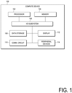
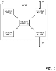
Technologies for a unified test and debug architecture
PatentPendingUS20240329129A1
Innovation
- A unified test and debug architecture is implemented using an external hardware debug interface that supports multiple protocols, including UCIe, JTAG, I2C, and PCIe, allowing debug messages to be sent and routed through a package with multiple chiplets, enabling interoperable debug/test solutions and facilitating infield debugging.
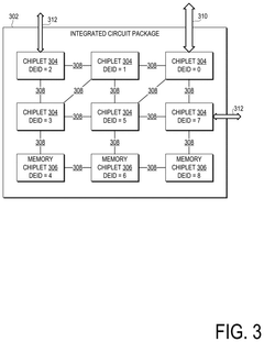
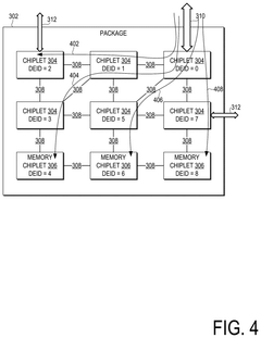
Non-homogeneous chiplets
PatentActiveUS12013810B2
Innovation
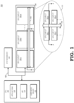
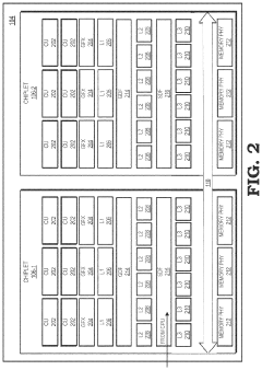
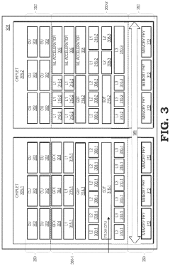
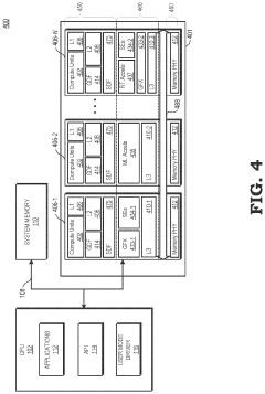
- The implementation of a semiconductor module with multiple interconnected GPU chiplets, each with a common set of circuitry modules and non-homogeneous supporting modules, allows for efficient distribution of workloads across chiplets, utilizing an interconnect that provides coherent memory access and routes commands to appropriate chiplets based on their specific capabilities.
Interoperability Challenges and Cross-vendor Compatibility
The interoperability landscape for chiplet integration presents significant challenges as the industry moves toward heterogeneous integration. Current standards like UCIe (Universal Chiplet Interconnect Express), AIB (Advanced Interface Bus), and BoW (Bunch of Wires) each employ different protocols, physical interfaces, and communication methodologies, creating substantial barriers to cross-vendor compatibility. These differences manifest in varying power requirements, signal integrity specifications, and thermal management approaches that complicate integration efforts.
When chiplets from different vendors are combined, interface mismatches often necessitate complex bridge components or adaptation layers, introducing additional latency, power consumption, and design complexity. These translation mechanisms can significantly diminish the performance benefits that chiplet architectures promise to deliver, particularly in high-bandwidth, low-latency applications such as AI accelerators and high-performance computing systems.
Testing and validation processes further complicate cross-vendor integration. The absence of standardized testing methodologies means that chiplets validated individually may still experience compatibility issues when integrated into a multi-vendor system. This uncertainty increases development cycles and raises costs as extensive system-level testing becomes necessary to ensure reliable operation.
IP protection and licensing considerations create additional friction in the chiplet ecosystem. Vendors must navigate complex agreements regarding interface specifications, often limiting the transparency needed for seamless integration. Some companies maintain proprietary interfaces to protect their competitive advantages, directly conflicting with the open ecosystem needed for true interoperability.
Supply chain dependencies represent another critical challenge. When systems rely on chiplets from multiple vendors, production schedules become vulnerable to disruptions in any single supplier's manufacturing capacity. This interdependence can lead to cascading delays and availability issues that affect entire product lines.
The industry has recognized these challenges and begun forming consortia like the UCIe Consortium and ODSA (Open Domain-Specific Architecture) to establish common standards. However, competing interests and technical disagreements have slowed progress toward a unified approach. The tension between standardization and innovation remains unresolved, as companies balance the benefits of ecosystem participation against the competitive advantages of proprietary solutions.
Addressing these interoperability challenges will require unprecedented collaboration across the semiconductor industry, potentially including the development of certification programs, reference designs, and open-source tools that facilitate cross-vendor integration while protecting intellectual property rights.
Economic Impact and Manufacturing Considerations for Chiplet Adoption
The economic implications of chiplet adoption extend far beyond technical considerations, representing a paradigm shift in semiconductor manufacturing economics. Cost analysis reveals that chiplet-based designs can reduce manufacturing expenses by 25-40% compared to monolithic approaches, primarily through improved yield rates. When fabricating large monolithic dies, even minor defects render entire chips unusable, whereas chiplet architectures isolate defects to individual components, significantly enhancing overall production yield and reducing waste.
Capital expenditure requirements present another compelling economic advantage. Traditional leading-edge fabs require investments exceeding $20 billion, creating substantial barriers to entry. Chiplet strategies allow companies to selectively invest in advanced nodes only for performance-critical components while utilizing mature, cost-effective processes for other elements, democratizing access to advanced semiconductor capabilities for mid-tier manufacturers.
Supply chain resilience has emerged as a critical consideration following recent global disruptions. Chiplet ecosystems enable geographic diversification of manufacturing, with different components potentially produced across multiple facilities or even countries. This distribution mitigates regional manufacturing risks and aligns with governmental initiatives promoting domestic semiconductor production capabilities.
Manufacturing considerations for chiplet adoption necessitate significant infrastructure adjustments. Assembly and packaging facilities require substantial upgrades to handle the precision demands of chiplet integration, with positioning accuracy requirements in the micron range. Advanced packaging techniques like silicon interposers and direct copper bonding demand specialized equipment investments and workforce retraining programs.
Testing methodologies must also evolve substantially. Traditional single-die testing approaches prove insufficient for chiplet architectures, necessitating new protocols for both pre-integration component validation and post-integration system verification. Known-good-die testing becomes particularly crucial, as defective chiplets identified post-integration result in disproportionately higher costs.
Environmental sustainability presents both challenges and opportunities. While chiplet approaches reduce silicon waste through improved yields, advanced packaging materials may introduce new environmental considerations. Life cycle assessments indicate that chiplet-based designs can reduce overall carbon footprints by 15-30% compared to equivalent monolithic implementations, primarily through manufacturing efficiency improvements and extended product lifespans enabled by modular upgradeability.
Unlock deeper insights with PatSnap Eureka Quick Research — get a full tech report to explore trends and direct your research. Try now!
Generate Your Research Report Instantly with AI Agent
Supercharge your innovation with PatSnap Eureka AI Agent Platform!