
Comparison of OLED vs MicroLED Electrode Materials
OCT 24, 20259 MIN READ
Generate Your Research Report Instantly with AI Agent
Patsnap Eureka helps you evaluate technical feasibility & market potential.
OLED and MicroLED Electrode Materials Background and Objectives
Display technologies have undergone significant evolution over the past decades, with OLED (Organic Light-Emitting Diode) establishing itself as a dominant technology in high-end displays since the early 2000s. More recently, MicroLED has emerged as a promising next-generation display technology, potentially offering advantages over OLED in several key performance metrics. At the heart of both technologies are electrode materials that play crucial roles in device efficiency, lifetime, and manufacturing complexity.
OLED technology utilizes organic compounds that emit light when an electric current passes through them. The technology has evolved from simple passive-matrix designs to active-matrix configurations, enabling higher resolution and better performance. The electrode materials in OLEDs typically consist of a transparent anode (commonly Indium Tin Oxide or ITO) and a reflective cathode (often aluminum with lithium fluoride layers), with organic layers sandwiched between them.
MicroLED, in contrast, employs inorganic semiconductor materials to create arrays of microscopic LEDs. Each pixel contains red, green, and blue micro-scale LEDs that directly emit colored light. The electrode configuration in MicroLEDs differs fundamentally from OLEDs, requiring materials that can support higher current densities while maintaining transparency where needed.
The historical development of electrode materials for both technologies reflects ongoing efforts to balance competing requirements: electrical conductivity, optical transparency, mechanical flexibility, chemical stability, and manufacturing cost. For OLEDs, significant milestones include the development of flexible transparent electrodes using materials like PEDOT:PSS and silver nanowires, enabling the creation of bendable and foldable displays.
For MicroLEDs, electrode material development has focused on addressing unique challenges such as efficient current spreading at microscale dimensions and managing heat dissipation. Recent innovations include advanced metal alloys and novel transparent conductive oxides designed specifically for the high-current operation of MicroLED pixels.
The technical objectives of this comparative analysis are to evaluate the performance characteristics, manufacturing considerations, and future potential of electrode materials for both OLED and MicroLED technologies. Specifically, we aim to assess conductivity-transparency trade-offs, processing compatibility with existing manufacturing infrastructure, long-term stability under operating conditions, and scalability to different display sizes and form factors.
Additionally, this analysis seeks to identify emerging electrode materials that could enable breakthrough performance in either technology, including graphene-based electrodes, metal mesh structures, and hybrid organic-inorganic composites. Understanding these materials is crucial for predicting future display technology trajectories and informing strategic R&D investments.
OLED technology utilizes organic compounds that emit light when an electric current passes through them. The technology has evolved from simple passive-matrix designs to active-matrix configurations, enabling higher resolution and better performance. The electrode materials in OLEDs typically consist of a transparent anode (commonly Indium Tin Oxide or ITO) and a reflective cathode (often aluminum with lithium fluoride layers), with organic layers sandwiched between them.
MicroLED, in contrast, employs inorganic semiconductor materials to create arrays of microscopic LEDs. Each pixel contains red, green, and blue micro-scale LEDs that directly emit colored light. The electrode configuration in MicroLEDs differs fundamentally from OLEDs, requiring materials that can support higher current densities while maintaining transparency where needed.
The historical development of electrode materials for both technologies reflects ongoing efforts to balance competing requirements: electrical conductivity, optical transparency, mechanical flexibility, chemical stability, and manufacturing cost. For OLEDs, significant milestones include the development of flexible transparent electrodes using materials like PEDOT:PSS and silver nanowires, enabling the creation of bendable and foldable displays.
For MicroLEDs, electrode material development has focused on addressing unique challenges such as efficient current spreading at microscale dimensions and managing heat dissipation. Recent innovations include advanced metal alloys and novel transparent conductive oxides designed specifically for the high-current operation of MicroLED pixels.
The technical objectives of this comparative analysis are to evaluate the performance characteristics, manufacturing considerations, and future potential of electrode materials for both OLED and MicroLED technologies. Specifically, we aim to assess conductivity-transparency trade-offs, processing compatibility with existing manufacturing infrastructure, long-term stability under operating conditions, and scalability to different display sizes and form factors.
Additionally, this analysis seeks to identify emerging electrode materials that could enable breakthrough performance in either technology, including graphene-based electrodes, metal mesh structures, and hybrid organic-inorganic composites. Understanding these materials is crucial for predicting future display technology trajectories and informing strategic R&D investments.
Market Demand Analysis for Advanced Display Technologies
The display technology market is experiencing a significant shift as advanced technologies like OLED and MicroLED gain prominence. Current market analysis indicates that the global display market is projected to reach $167 billion by 2025, with OLED and MicroLED technologies accounting for an increasingly substantial portion of this growth. Consumer electronics, particularly smartphones and televisions, remain the primary drivers of demand for these advanced display technologies.
OLED technology has established a strong market presence, particularly in premium smartphones and high-end televisions. The demand for OLED displays has been steadily increasing due to their superior color reproduction, contrast ratios, and form factor flexibility. This growth is further accelerated by the expanding market for foldable and rollable displays, where OLED's inherent flexibility provides a significant competitive advantage.
MicroLED technology, though still in its early commercialization stages, is generating substantial market interest due to its potential advantages over OLED, including higher brightness, longer lifespan, and better energy efficiency. Market research indicates growing demand for MicroLED in specialized applications such as AR/VR headsets, automotive displays, and ultra-large-format displays where its superior brightness and durability offer distinct advantages.
The electrode materials used in both technologies represent a critical component affecting performance, manufacturing costs, and environmental impact. Market demand for transparent conductive materials has evolved significantly, with indium tin oxide (ITO) traditionally dominating the OLED market despite its brittleness and limited flexibility. Alternative materials such as silver nanowires, graphene, and metal meshes are gaining traction as the market increasingly demands flexible and foldable displays.
For MicroLED displays, electrode material requirements differ substantially, with emphasis on materials that can support higher current densities and offer enhanced thermal management properties. This has created new market opportunities for specialized conductive materials optimized for MicroLED applications.
Regional analysis shows Asia-Pacific leading the market demand for advanced display technologies, with South Korea, Japan, China, and Taiwan hosting major manufacturing facilities. North America and Europe represent significant consumer markets, particularly for premium display products incorporating cutting-edge electrode materials.
Industry forecasts suggest that environmental considerations will increasingly influence market demand, with growing preference for electrode materials that reduce reliance on rare elements like indium and offer improved recyclability. This trend aligns with broader sustainability initiatives across the consumer electronics industry and represents an important factor in future market development for both OLED and MicroLED electrode materials.
OLED technology has established a strong market presence, particularly in premium smartphones and high-end televisions. The demand for OLED displays has been steadily increasing due to their superior color reproduction, contrast ratios, and form factor flexibility. This growth is further accelerated by the expanding market for foldable and rollable displays, where OLED's inherent flexibility provides a significant competitive advantage.
MicroLED technology, though still in its early commercialization stages, is generating substantial market interest due to its potential advantages over OLED, including higher brightness, longer lifespan, and better energy efficiency. Market research indicates growing demand for MicroLED in specialized applications such as AR/VR headsets, automotive displays, and ultra-large-format displays where its superior brightness and durability offer distinct advantages.
The electrode materials used in both technologies represent a critical component affecting performance, manufacturing costs, and environmental impact. Market demand for transparent conductive materials has evolved significantly, with indium tin oxide (ITO) traditionally dominating the OLED market despite its brittleness and limited flexibility. Alternative materials such as silver nanowires, graphene, and metal meshes are gaining traction as the market increasingly demands flexible and foldable displays.
For MicroLED displays, electrode material requirements differ substantially, with emphasis on materials that can support higher current densities and offer enhanced thermal management properties. This has created new market opportunities for specialized conductive materials optimized for MicroLED applications.
Regional analysis shows Asia-Pacific leading the market demand for advanced display technologies, with South Korea, Japan, China, and Taiwan hosting major manufacturing facilities. North America and Europe represent significant consumer markets, particularly for premium display products incorporating cutting-edge electrode materials.
Industry forecasts suggest that environmental considerations will increasingly influence market demand, with growing preference for electrode materials that reduce reliance on rare elements like indium and offer improved recyclability. This trend aligns with broader sustainability initiatives across the consumer electronics industry and represents an important factor in future market development for both OLED and MicroLED electrode materials.
Current State and Challenges in Electrode Material Development
The electrode materials landscape for both OLED and MicroLED technologies has evolved significantly in recent years, with each technology presenting unique challenges and opportunities. Currently, OLED electrode development is dominated by indium tin oxide (ITO) as the transparent conductive electrode material, which offers good transparency and conductivity. However, ITO faces limitations including brittleness, limited flexibility, and the scarcity of indium resources, driving research toward alternative materials.
For OLED applications, emerging alternatives include silver nanowires, carbon nanotubes, graphene, and PEDOT:PSS conductive polymers. These materials show promise in addressing flexibility requirements for next-generation displays but face challenges in achieving the optimal balance between transparency, conductivity, and long-term stability. Silver nanowire networks, while offering excellent conductivity, struggle with surface roughness issues that can lead to device shorting.
MicroLED electrode materials face different challenges compared to OLEDs. The miniaturization of LED structures to microscale dimensions requires electrode materials with exceptional precision in deposition and patterning capabilities. Current approaches utilize metal stacks including aluminum, titanium, and gold for contacts, but achieving uniform current distribution across ultra-small pixel areas remains problematic.
A significant challenge for both technologies is the trade-off between optical transparency and electrical conductivity. This is particularly critical for MicroLED, where light extraction efficiency directly impacts overall device performance. The development of transparent conductive oxides with improved conductivity and transparency is ongoing, with materials like aluminum-doped zinc oxide (AZO) and fluorine-doped tin oxide (FTO) showing potential.
Manufacturing scalability presents another major hurdle. While OLED electrode deposition has benefited from years of process optimization, MicroLED electrode fabrication requires new approaches compatible with mass transfer processes. The industry is exploring techniques such as selective area deposition and advanced lithography to address these challenges.
Stability under operational conditions differs significantly between technologies. OLED electrodes must withstand organic layer degradation mechanisms, while MicroLED electrodes face thermal management challenges due to higher current densities. This has prompted research into barrier materials and interface engineering to enhance electrode longevity in both technologies.
Geographically, electrode material development shows distinct patterns, with East Asian countries (particularly South Korea, Japan, and China) leading OLED electrode innovation, while MicroLED electrode research demonstrates a more distributed pattern across North America, Europe, and Asia, reflecting the emerging nature of the technology.
For OLED applications, emerging alternatives include silver nanowires, carbon nanotubes, graphene, and PEDOT:PSS conductive polymers. These materials show promise in addressing flexibility requirements for next-generation displays but face challenges in achieving the optimal balance between transparency, conductivity, and long-term stability. Silver nanowire networks, while offering excellent conductivity, struggle with surface roughness issues that can lead to device shorting.
MicroLED electrode materials face different challenges compared to OLEDs. The miniaturization of LED structures to microscale dimensions requires electrode materials with exceptional precision in deposition and patterning capabilities. Current approaches utilize metal stacks including aluminum, titanium, and gold for contacts, but achieving uniform current distribution across ultra-small pixel areas remains problematic.
A significant challenge for both technologies is the trade-off between optical transparency and electrical conductivity. This is particularly critical for MicroLED, where light extraction efficiency directly impacts overall device performance. The development of transparent conductive oxides with improved conductivity and transparency is ongoing, with materials like aluminum-doped zinc oxide (AZO) and fluorine-doped tin oxide (FTO) showing potential.
Manufacturing scalability presents another major hurdle. While OLED electrode deposition has benefited from years of process optimization, MicroLED electrode fabrication requires new approaches compatible with mass transfer processes. The industry is exploring techniques such as selective area deposition and advanced lithography to address these challenges.
Stability under operational conditions differs significantly between technologies. OLED electrodes must withstand organic layer degradation mechanisms, while MicroLED electrodes face thermal management challenges due to higher current densities. This has prompted research into barrier materials and interface engineering to enhance electrode longevity in both technologies.
Geographically, electrode material development shows distinct patterns, with East Asian countries (particularly South Korea, Japan, and China) leading OLED electrode innovation, while MicroLED electrode research demonstrates a more distributed pattern across North America, Europe, and Asia, reflecting the emerging nature of the technology.
Current Electrode Material Solutions Comparison
01 Transparent conductive oxide electrodes for OLED and MicroLED
Transparent conductive oxide (TCO) materials are widely used as electrode materials in OLED and MicroLED devices due to their combination of optical transparency and electrical conductivity. Common TCO materials include indium tin oxide (ITO), zinc oxide (ZnO), and aluminum-doped zinc oxide (AZO). These materials allow light to pass through while providing the necessary electrical conductivity for device operation. TCO electrodes are typically used as anodes in display applications where light must be transmitted through the electrode.- Transparent conductive materials for OLED/MicroLED electrodes: Transparent conductive materials are essential for electrode applications in OLED and MicroLED displays, particularly for the anode which must allow light to pass through. Indium tin oxide (ITO) is commonly used due to its high transparency and conductivity. Alternative materials include conductive polymers, metal nanowires, graphene, and carbon nanotubes, which offer flexibility advantages over traditional ITO. These materials enable the development of flexible and transparent display technologies while maintaining electrical performance.
- Metal and metal alloy electrodes for improved efficiency: Metal and metal alloy electrodes are widely used in OLED and MicroLED devices to enhance electrical conductivity and device efficiency. Materials such as aluminum, silver, gold, and their alloys are commonly employed as cathode materials due to their low work function and high reflectivity. These properties help improve electron injection and light extraction efficiency. Multilayer metal structures can be designed to optimize both electrical performance and optical properties, resulting in devices with higher brightness and lower power consumption.
- Nanostructured electrode materials for enhanced performance: Nanostructured electrode materials offer significant advantages for OLED and MicroLED applications, including increased surface area, improved charge transport, and enhanced light extraction. These materials include metal nanoparticles, nanowires, and nanocomposites that can be engineered to optimize specific properties. Nanostructured electrodes can reduce interface resistance, improve current spreading, and enhance device stability. The controlled morphology at the nanoscale allows for precise tuning of optical and electrical properties, leading to more efficient and longer-lasting display devices.
- Composite and hybrid electrode materials: Composite and hybrid electrode materials combine different types of conductive materials to achieve superior performance characteristics for OLED and MicroLED applications. These materials typically integrate organic and inorganic components or different classes of conductors to overcome limitations of single-material electrodes. Examples include polymer-metal composites, carbon-based materials with metal nanoparticles, and oxide-metal multilayers. These hybrid structures can offer improved flexibility, conductivity, transparency, and stability compared to conventional electrode materials, enabling advanced display technologies with enhanced performance and durability.
- Electrode interface engineering and buffer layers: Electrode interface engineering and buffer layers play a crucial role in optimizing charge injection and extraction in OLED and MicroLED devices. Various materials are used as buffer layers between the electrodes and the emissive layers to improve energy level alignment, reduce barriers to charge transport, and enhance device stability. Common buffer materials include metal oxides, organic semiconductors, and ultrathin metal films. Proper interface engineering can significantly improve device efficiency, operational lifetime, and reduce degradation mechanisms, resulting in higher performance displays with better color accuracy and longevity.
02 Metal and metal alloy electrodes for enhanced conductivity
Metal and metal alloy electrodes offer superior electrical conductivity compared to other electrode materials, making them ideal for applications requiring low resistance and high current density. Common metals used include aluminum, silver, gold, and copper, as well as various alloys. These materials are often used as cathodes in OLED and MicroLED devices. While metals typically lack transparency, they can be made into ultra-thin films or patterned grids to balance conductivity with optical requirements. Advanced deposition techniques help achieve uniform metal electrode layers with minimal defects.Expand Specific Solutions03 Carbon-based electrode materials
Carbon-based materials such as graphene, carbon nanotubes (CNTs), and conductive polymers offer unique advantages as electrode materials for OLED and MicroLED applications. These materials combine flexibility, transparency, and conductivity, making them suitable for next-generation flexible displays. Carbon-based electrodes can be solution-processed, enabling low-cost manufacturing methods like printing. Additionally, these materials can be engineered to have work functions compatible with various emissive layers, improving charge injection efficiency and device performance.Expand Specific Solutions04 Composite and multilayer electrode structures
Composite and multilayer electrode structures combine different materials to achieve optimal electrical, optical, and mechanical properties for OLED and MicroLED applications. These structures often include combinations of metals, transparent conductive oxides, and organic materials arranged in strategic layers. Common configurations include metal/TCO bilayers or metal grid/conductive polymer hybrids. These composite electrodes can be engineered to enhance light extraction, improve charge injection, reduce resistance, and increase device stability while maintaining necessary transparency or reflectivity.Expand Specific Solutions05 Novel electrode materials for improved device performance
Research into novel electrode materials aims to overcome limitations of conventional electrodes in OLED and MicroLED devices. These include silver nanowires, metal meshes, conductive metal-organic frameworks, and doped semiconductors. These materials offer advantages such as enhanced flexibility, improved transparency-to-conductivity ratios, better compatibility with emissive layers, and simplified manufacturing processes. Some novel materials also address issues like work function matching, interface stability, and environmental durability, leading to devices with longer lifetimes and higher efficiency.Expand Specific Solutions
Key Industry Players in OLED and MicroLED Manufacturing
The OLED vs MicroLED electrode materials market is currently in a transitional phase, with OLED technology reaching maturity while MicroLED remains in early commercialization stages. The global display materials market is projected to exceed $30 billion by 2025, with electrode materials representing a significant segment. In terms of technical maturity, companies like Samsung, LG Display, and Universal Display Corporation lead OLED electrode innovation with established manufacturing processes, while BOE Technology and Lumileds are advancing MicroLED electrode materials. Companies including Applied Materials and Intel are developing next-generation transparent conductive materials for both technologies, focusing on improving efficiency, flexibility, and reducing rare metal dependency. The competitive landscape is intensifying as MicroLED approaches commercial viability, challenging OLED's current market dominance.
BOE Technology Group Co., Ltd.
Technical Solution: BOE has developed comprehensive electrode solutions for both OLED and MicroLED technologies. For OLED displays, BOE employs a hybrid electrode system combining indium tin oxide (ITO) with silver nanowire networks, achieving sheet resistance below 15 ohms/square while maintaining transparency above 85%. Their patented electrode structure incorporates specialized buffer layers that enhance charge injection efficiency and improve operational stability. For MicroLED displays, BOE has pioneered a unique electrode architecture using copper-based microgrids with line widths below 2μm and specialized passivation techniques to prevent oxidation. Their MicroLED electrode design features a proprietary current spreading layer that ensures uniform brightness across each pixel, critical for high-resolution displays. BOE has also developed a novel manufacturing process for their electrode materials that reduces production steps by approximately 30% compared to conventional methods, significantly lowering manufacturing costs while maintaining performance specifications.
Strengths: BOE's electrode materials demonstrate excellent cost-efficiency ratio, making them suitable for mass-market applications. Their manufacturing processes for electrode deposition show high throughput and scalability for large panel production. Weaknesses: Their electrode materials may show slightly lower conductivity compared to premium competitors, potentially affecting power efficiency in high-brightness applications. The long-term stability of their electrode materials under extreme operating conditions remains less proven than some industry veterans.
LG Display Co., Ltd.
Technical Solution: LG Display has developed distinctive electrode technologies for both display types. For OLED, LG utilizes a proprietary transparent conductive oxide (TCO) electrode system that combines indium tin oxide with zinc oxide dopants to achieve conductivity of approximately 5×10^4 S/cm while maintaining over 88% transparency. Their OLED electrodes feature a multi-layer structure with silver nanowire networks embedded in conductive polymers, allowing for flexibility while reducing sheet resistance to below 10 ohms/square. For MicroLED displays, LG has pioneered a unique electrode architecture using copper-based metal mesh technology with line widths below 1μm, making them virtually invisible to the naked eye. Their MicroLED electrodes incorporate specialized diffusion barrier layers that prevent metal migration and enhance long-term reliability. LG has also developed a proprietary surface treatment process for their MicroLED electrodes that improves the interface with the emissive material, reducing operating voltage by approximately 15% compared to conventional designs.
Strengths: LG's electrode materials offer excellent balance between transparency and conductivity, particularly important for large-format displays. Their copper-based electrode technology for MicroLEDs provides cost advantages over gold or silver alternatives. Weaknesses: The complex multi-layer electrode structures require precise manufacturing controls, potentially affecting yield rates. Their OLED electrode materials may show faster degradation under high brightness conditions compared to some competitors.
Critical Technical Analysis of Electrode Material Patents
Thermal active delay fluorescent material, method for manufacturing same, and organic light-emitting diode device
PatentActiveUS20200331923A1
Innovation
- A deep red light TADF material with ultrafast reverse intersystem crossing speed and high luminous efficiency is developed, utilizing a chemical structure combining a strong electron donor and acceptor, manufactured through a specific synthesis process involving NaH, dehydrogenation, and column chromatography purification, to achieve 100% internal quantum efficiency.


Organic light emitting diode and organic light emitting device including the same
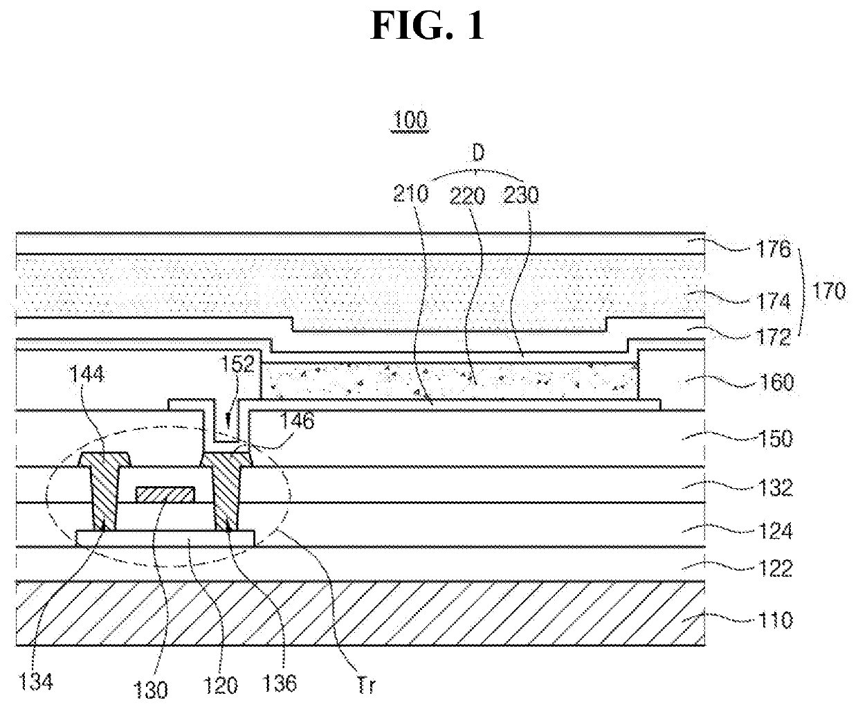
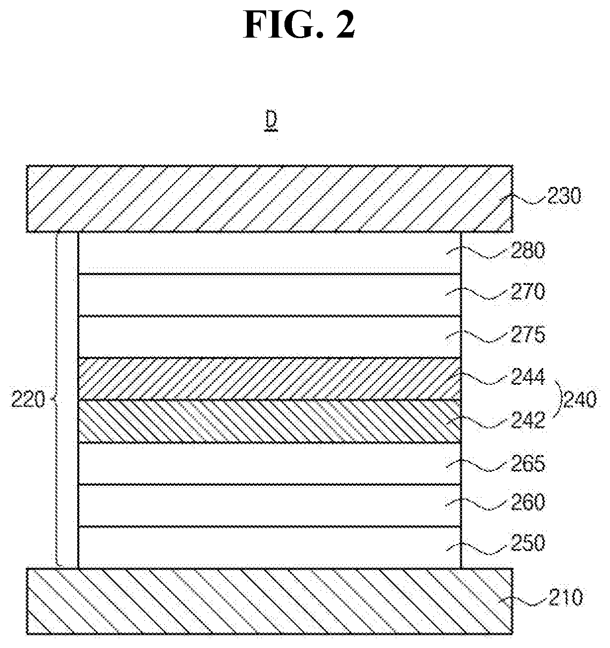
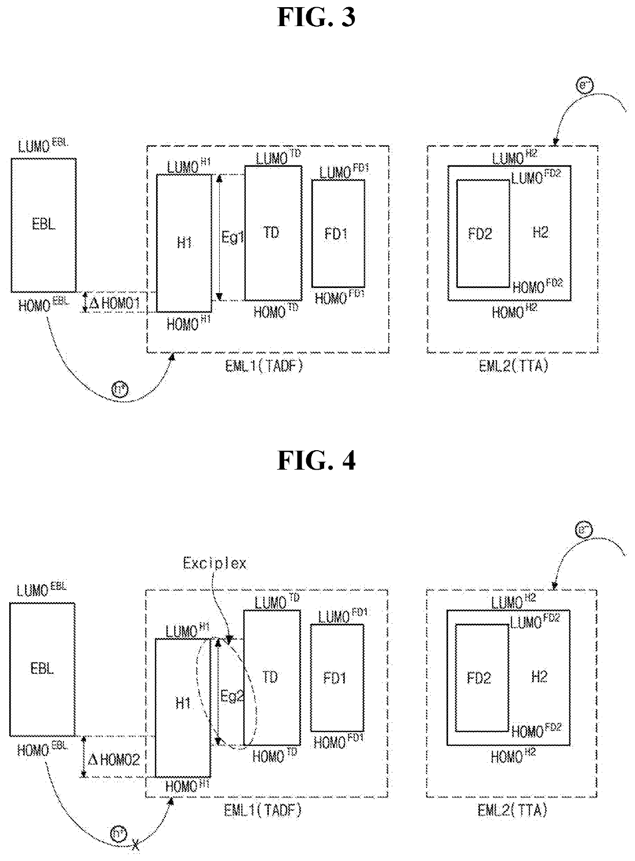
PatentActiveUS20210126205A1
Innovation
- The OLED design incorporates multiple emitting material layers with specific organic compounds, including a first and second emitting material layer with compounds having specific structures, to achieve thermally activated delayed fluorescence and triplet-triplet annihilation, optimizing energy levels for efficient exciton transfer and prolonged luminous efficiency.

Environmental Impact and Sustainability Considerations
The environmental footprint of display technologies has become increasingly important as sustainability considerations gain prominence in consumer electronics. OLED and MicroLED technologies differ significantly in their environmental impact, particularly regarding their electrode materials and manufacturing processes.
OLED displays typically utilize indium tin oxide (ITO) as the primary transparent electrode material, which presents several environmental challenges. Indium is a rare earth element with limited global reserves, raising concerns about resource depletion. The extraction and processing of indium involve energy-intensive mining operations that generate significant carbon emissions and can lead to habitat destruction. Additionally, the chemical processes used to deposit ITO layers often employ hazardous substances that require careful handling and disposal.
In contrast, MicroLED technology offers potential environmental advantages through its electrode material choices. Many MicroLED designs utilize aluminum or copper-based conductors that are more abundant and less environmentally problematic to source than indium. These materials generally have well-established recycling infrastructures, potentially enabling better end-of-life recovery. However, MicroLED manufacturing currently requires more complex fabrication steps, which can offset some of these material advantages through increased energy consumption.
Energy efficiency during operation represents another critical environmental consideration. OLED displays consume less power when displaying darker content due to their emissive nature, while MicroLED technology promises even greater efficiency across all brightness levels. This improved efficiency translates directly to reduced carbon emissions over the product lifecycle, particularly as displays grow larger and more prevalent in various applications.
End-of-life management presents distinct challenges for both technologies. OLED displays contain organic materials that can be difficult to separate and recycle effectively. The electrode materials in OLEDs, particularly those containing indium, represent valuable resources that are currently under-recovered. MicroLED displays may offer better recyclability due to their predominantly inorganic composition and potentially simpler material separation, though the industry has yet to establish large-scale recycling processes for either technology.
Manufacturing waste generation differs significantly between the technologies. OLED production typically involves solution-based processes that generate chemical waste requiring specialized treatment. MicroLED manufacturing currently suffers from yield challenges that result in material wastage, though advances in production techniques are gradually improving efficiency. Both technologies are moving toward more sustainable manufacturing approaches, including reduced solvent usage and improved material utilization.
OLED displays typically utilize indium tin oxide (ITO) as the primary transparent electrode material, which presents several environmental challenges. Indium is a rare earth element with limited global reserves, raising concerns about resource depletion. The extraction and processing of indium involve energy-intensive mining operations that generate significant carbon emissions and can lead to habitat destruction. Additionally, the chemical processes used to deposit ITO layers often employ hazardous substances that require careful handling and disposal.
In contrast, MicroLED technology offers potential environmental advantages through its electrode material choices. Many MicroLED designs utilize aluminum or copper-based conductors that are more abundant and less environmentally problematic to source than indium. These materials generally have well-established recycling infrastructures, potentially enabling better end-of-life recovery. However, MicroLED manufacturing currently requires more complex fabrication steps, which can offset some of these material advantages through increased energy consumption.
Energy efficiency during operation represents another critical environmental consideration. OLED displays consume less power when displaying darker content due to their emissive nature, while MicroLED technology promises even greater efficiency across all brightness levels. This improved efficiency translates directly to reduced carbon emissions over the product lifecycle, particularly as displays grow larger and more prevalent in various applications.
End-of-life management presents distinct challenges for both technologies. OLED displays contain organic materials that can be difficult to separate and recycle effectively. The electrode materials in OLEDs, particularly those containing indium, represent valuable resources that are currently under-recovered. MicroLED displays may offer better recyclability due to their predominantly inorganic composition and potentially simpler material separation, though the industry has yet to establish large-scale recycling processes for either technology.
Manufacturing waste generation differs significantly between the technologies. OLED production typically involves solution-based processes that generate chemical waste requiring specialized treatment. MicroLED manufacturing currently suffers from yield challenges that result in material wastage, though advances in production techniques are gradually improving efficiency. Both technologies are moving toward more sustainable manufacturing approaches, including reduced solvent usage and improved material utilization.
Manufacturing Scalability and Cost Analysis
The manufacturing scalability and cost analysis of electrode materials represents a critical factor in the commercial viability of both OLED and MicroLED technologies. OLED manufacturing has matured significantly over the past decade, with established production lines utilizing vacuum thermal evaporation for small molecule OLEDs and solution processing for polymer-based variants. The electrode materials, primarily ITO (Indium Tin Oxide) and alternative transparent conductive oxides, benefit from economies of scale and established supply chains, resulting in relatively stable costs despite indium's limited availability.
In contrast, MicroLED electrode manufacturing faces substantial challenges in scaling to mass production. The process requires precise deposition of conductive materials on microscopic LED structures, often necessitating advanced lithography techniques and specialized equipment. Current manufacturing approaches include photolithography, inkjet printing, and laser-assisted patterning, each with varying degrees of throughput and precision. The complexity of these processes contributes significantly to the overall higher production costs of MicroLED displays compared to OLEDs.
Cost analysis reveals that electrode materials constitute approximately 15-20% of total material costs in OLED production, whereas for MicroLED, this figure ranges from 25-30% due to more complex electrode architectures and higher precision requirements. The yield rates further amplify this cost differential, with OLED manufacturing achieving industry-standard yields of 70-85% while MicroLED production currently struggles with yields below 60% for high-resolution applications.
Recent advancements in roll-to-roll processing for flexible electrodes show promise for reducing OLED production costs by an estimated 30-40% over the next five years. Meanwhile, MicroLED manufacturing is exploring mass transfer techniques and improved electrode deposition methods that could potentially reduce costs by 50-60%, though from a much higher baseline.
Energy consumption during manufacturing presents another significant cost factor. OLED electrode deposition typically requires 1.2-1.8 kWh per square meter of display area, while MicroLED electrode processing consumes 2.5-3.5 kWh for equivalent output due to more energy-intensive precision processes. This energy differential translates to approximately 15% higher operational costs for MicroLED electrode manufacturing.
Supply chain considerations also impact scalability, with OLED electrode materials benefiting from established global suppliers and relatively stable pricing. MicroLED electrode materials, particularly specialized conductive nanoparticles and advanced metal alloys, face more volatile supply conditions and pricing structures, introducing additional uncertainty to manufacturing cost projections and potentially limiting rapid production scaling.
In contrast, MicroLED electrode manufacturing faces substantial challenges in scaling to mass production. The process requires precise deposition of conductive materials on microscopic LED structures, often necessitating advanced lithography techniques and specialized equipment. Current manufacturing approaches include photolithography, inkjet printing, and laser-assisted patterning, each with varying degrees of throughput and precision. The complexity of these processes contributes significantly to the overall higher production costs of MicroLED displays compared to OLEDs.
Cost analysis reveals that electrode materials constitute approximately 15-20% of total material costs in OLED production, whereas for MicroLED, this figure ranges from 25-30% due to more complex electrode architectures and higher precision requirements. The yield rates further amplify this cost differential, with OLED manufacturing achieving industry-standard yields of 70-85% while MicroLED production currently struggles with yields below 60% for high-resolution applications.
Recent advancements in roll-to-roll processing for flexible electrodes show promise for reducing OLED production costs by an estimated 30-40% over the next five years. Meanwhile, MicroLED manufacturing is exploring mass transfer techniques and improved electrode deposition methods that could potentially reduce costs by 50-60%, though from a much higher baseline.
Energy consumption during manufacturing presents another significant cost factor. OLED electrode deposition typically requires 1.2-1.8 kWh per square meter of display area, while MicroLED electrode processing consumes 2.5-3.5 kWh for equivalent output due to more energy-intensive precision processes. This energy differential translates to approximately 15% higher operational costs for MicroLED electrode manufacturing.
Supply chain considerations also impact scalability, with OLED electrode materials benefiting from established global suppliers and relatively stable pricing. MicroLED electrode materials, particularly specialized conductive nanoparticles and advanced metal alloys, face more volatile supply conditions and pricing structures, introducing additional uncertainty to manufacturing cost projections and potentially limiting rapid production scaling.
Unlock deeper insights with Patsnap Eureka Quick Research — get a full tech report to explore trends and direct your research. Try now!
Generate Your Research Report Instantly with AI Agent
Supercharge your innovation with Patsnap Eureka AI Agent Platform!