Comparison of Photonic Integrated Circuits vs Fiber Optics
SEP 29, 20259 MIN READ
Generate Your Research Report Instantly with AI Agent
Patsnap Eureka helps you evaluate technical feasibility & market potential.
PIC vs Fiber Optics: Evolution and Objectives
The evolution of optical communication technologies represents one of the most significant advancements in modern telecommunications. Fiber optics, introduced commercially in the 1970s, revolutionized data transmission by enabling high-bandwidth, long-distance communication through the propagation of light signals along thin strands of glass or plastic. This technology has formed the backbone of global telecommunications infrastructure for decades, continuously evolving to support increasing bandwidth demands.
Photonic Integrated Circuits (PICs) emerged as the next evolutionary step, applying the principles of electronic integration to photonic components. Beginning in the early 2000s, PICs have gained momentum as a technology that promises to overcome the physical limitations of traditional fiber optics while offering unprecedented levels of integration, miniaturization, and energy efficiency.
The historical trajectory of both technologies reveals a pattern of continuous innovation driven by increasing data transmission requirements. Fiber optics evolved from simple point-to-point connections to complex wavelength division multiplexing (WDM) systems capable of transmitting multiple data streams simultaneously. Similarly, PICs have progressed from basic components to sophisticated systems integrating hundreds of optical elements on a single chip.
Current technological objectives in this field focus on addressing the exponential growth in data traffic while managing power consumption and physical space constraints. PICs aim to achieve higher integration densities, reduced power consumption, and enhanced functionality through the incorporation of multiple optical functions on a single substrate. Meanwhile, fiber optic technology continues to pursue higher transmission capacities through advanced modulation schemes and specialized fiber designs.
The convergence of these technologies presents unique opportunities and challenges. While fiber optics excel in long-distance transmission with minimal signal degradation, PICs offer advantages in compact, energy-efficient processing nodes. The ultimate technological goal appears to be a hybrid approach that leverages the strengths of both technologies: using fiber optics for long-haul transmission and PICs for complex signal processing and routing at network nodes.
Looking forward, research objectives include developing seamless interfaces between fiber optics and PICs, enhancing the manufacturing scalability of photonic integrated circuits, and exploring novel materials that can further improve performance characteristics. The evolution of these complementary technologies will likely define the future landscape of optical communications, data centers, and emerging applications in quantum computing and sensing.
Market Demand Analysis for Integrated Photonics
The integrated photonics market is experiencing robust growth, driven by increasing demand for high-speed data transmission and processing capabilities across multiple industries. Current market projections indicate that the global photonic integrated circuit market is expected to reach $3.2 billion by 2027, growing at a CAGR of 25.3% from 2022 to 2027. This significant growth trajectory reflects the expanding applications of integrated photonics beyond traditional telecommunications.
Telecommunications remains the primary driver of market demand, accounting for approximately 40% of the total market share. The exponential increase in global data traffic, fueled by cloud computing, video streaming, and the proliferation of connected devices, necessitates higher bandwidth solutions that integrated photonics can deliver. Major telecom operators are actively investing in photonic integrated circuit technologies to enhance their network infrastructure.
Data centers represent another substantial market segment, with demand growing at nearly 30% annually. As hyperscale data centers expand to accommodate cloud services, they require energy-efficient solutions for interconnects. Photonic integrated circuits offer significant advantages over traditional fiber optics in this context, reducing power consumption by up to 70% while increasing data throughput.
The emerging application of integrated photonics in sensing and biomedical devices is creating new market opportunities. The biosensing market segment is projected to grow at 35% annually, as photonic integrated circuits enable more compact, sensitive, and cost-effective diagnostic tools. Healthcare providers are increasingly adopting these technologies for point-of-care testing and continuous patient monitoring.
Automotive and aerospace industries are also showing increased interest in integrated photonics for LiDAR systems and high-speed onboard communications. The automotive segment alone is expected to contribute $450 million to the market by 2027, primarily driven by autonomous vehicle development.
Regional analysis reveals that North America currently leads the market with 38% share, followed by Europe (29%) and Asia-Pacific (27%). However, the Asia-Pacific region is demonstrating the fastest growth rate at 28% annually, primarily due to substantial investments in telecommunications infrastructure and manufacturing capabilities in China, Japan, and South Korea.
Customer demand is increasingly focused on miniaturization, integration with electronic components, and cost reduction. End-users are seeking complete photonic systems-on-chip rather than discrete components, driving manufacturers toward higher levels of integration and functionality. This trend is particularly evident in consumer electronics applications, where space constraints and energy efficiency are critical considerations.
Technical Challenges in PIC and Fiber Optic Systems
Despite the significant advancements in both Photonic Integrated Circuits (PICs) and fiber optic technologies, numerous technical challenges persist that limit their full potential. For PICs, one of the most significant hurdles remains the integration complexity of multiple photonic components on a single chip. The precise alignment requirements at nanometer scales create substantial manufacturing difficulties, resulting in lower yields and higher production costs compared to electronic integrated circuits.
Material limitations represent another critical challenge for PICs. Silicon, while compatible with CMOS fabrication processes, exhibits inherent limitations in light emission capabilities. This necessitates the integration of different materials like III-V semiconductors, which introduces additional complexity in fabrication processes and potential interface issues between dissimilar materials.
Thermal management presents ongoing difficulties in PIC systems. Photonic components are often temperature-sensitive, with performance characteristics that can drift significantly with temperature variations. This necessitates sophisticated thermal control systems, adding complexity and cost to PIC implementations.
For fiber optic systems, signal attenuation over long distances remains a persistent challenge despite significant improvements. While modern fibers achieve impressive low-loss performance, ultra-long-haul applications still require periodic signal regeneration or amplification, increasing system complexity and cost.
Dispersion effects in fiber optics continue to limit maximum data rates and transmission distances. Chromatic dispersion causes different wavelengths to travel at slightly different speeds, resulting in pulse broadening and potential signal degradation. Modal dispersion in multimode fibers similarly restricts bandwidth-distance products.
The physical handling of fiber optic cables presents practical challenges in field deployments. Minimum bend radius limitations, connector reliability issues, and fiber fragility concerns impact installation and maintenance operations, particularly in harsh environments or space-constrained applications.
Both technologies face significant challenges in achieving cost-effective scaling. For PICs, the absence of standardized design tools, fabrication processes, and packaging solutions hampers mass production capabilities. Fiber optic systems struggle with installation costs, particularly in last-mile deployments where civil engineering work often dominates the expense profile.
Interfacing between electronic and photonic domains represents a common challenge for both technologies. The efficient conversion between electrical and optical signals requires specialized components that add complexity, power consumption, and potential performance bottlenecks to overall system designs.
Looking forward, addressing these technical challenges will require interdisciplinary approaches combining materials science, manufacturing engineering, thermal management, and system-level design optimization to fully realize the potential of both PIC and fiber optic technologies in next-generation communication systems.
Current Implementation Approaches for Both Technologies
01 Integration of photonic circuits with fiber optics
Photonic integrated circuits (PICs) can be seamlessly integrated with fiber optic systems to enhance data transmission capabilities. This integration involves coupling light between optical fibers and on-chip waveguides, enabling efficient signal transfer between fiber optic networks and integrated photonic components. Advanced coupling techniques minimize insertion losses and maximize bandwidth, creating hybrid systems that leverage the advantages of both technologies for telecommunications, data centers, and sensing applications.- Integration of photonic circuits with fiber optics: Photonic integrated circuits (PICs) can be seamlessly integrated with fiber optic systems to enhance data transmission capabilities. This integration involves coupling light between optical fibers and on-chip waveguides, enabling efficient signal transfer between fiber optic networks and integrated photonic components. Advanced coupling techniques minimize insertion losses and maximize bandwidth, creating high-performance optical communication systems that combine the advantages of both technologies.
- Silicon photonics for high-speed data transmission: Silicon photonics technology enables the fabrication of photonic integrated circuits on silicon substrates, leveraging existing semiconductor manufacturing processes. These circuits incorporate various optical components such as modulators, detectors, and multiplexers on a single chip for high-speed data transmission. The integration of silicon photonics with fiber optic systems allows for compact, energy-efficient solutions that can handle increasing bandwidth demands in telecommunications and data center applications.
- Optical signal processing and routing techniques: Advanced optical signal processing and routing techniques in photonic integrated circuits enable complex manipulation of light signals without conversion to electrical domain. These techniques include wavelength division multiplexing, optical switching, and signal regeneration implemented directly on photonic chips. By integrating these functionalities with fiber optic networks, the systems can achieve higher throughput, lower latency, and improved signal quality for next-generation optical communication networks.
- Novel materials and fabrication methods for PICs: Innovative materials and fabrication methods are being developed to enhance the performance of photonic integrated circuits and their compatibility with fiber optic systems. These include the use of III-V semiconductors, lithium niobate, polymers, and hybrid integration approaches. Advanced fabrication techniques such as nanoimprint lithography, 3D printing, and heterogeneous integration enable the creation of complex photonic structures with improved optical properties, leading to better coupling efficiency with optical fibers and enhanced overall system performance.
- Sensing and measurement applications: Photonic integrated circuits combined with fiber optics enable advanced sensing and measurement applications. These integrated systems can be used for high-precision temperature, pressure, and strain sensing, as well as chemical and biological detection. The combination of on-chip photonic components with fiber optic delivery systems allows for remote sensing capabilities, distributed measurement networks, and miniaturized sensor solutions with high sensitivity and reliability for various industrial, medical, and environmental monitoring applications.
02 Silicon photonics for high-speed optical communication
Silicon photonics technology enables the fabrication of photonic integrated circuits on silicon substrates, leveraging existing semiconductor manufacturing processes. These circuits incorporate various optical components such as modulators, detectors, and multiplexers on a single chip to achieve high-speed optical communication. The integration density and compatibility with CMOS technology make silicon photonics particularly suitable for data center interconnects, high-performance computing, and telecommunications applications where high bandwidth and energy efficiency are critical requirements.Expand Specific Solutions03 Novel waveguide structures for photonic integrated circuits
Advanced waveguide structures are fundamental components in photonic integrated circuits, guiding light with minimal losses and enabling complex optical functionalities. These structures include strip waveguides, rib waveguides, slot waveguides, and photonic crystal waveguides, each offering specific advantages for different applications. Novel designs incorporate materials with tailored refractive indices, specialized geometries, and innovative fabrication techniques to achieve improved light confinement, reduced propagation losses, and enhanced nonlinear optical effects for signal processing applications.Expand Specific Solutions04 Optical signal processing and modulation techniques
Advanced optical signal processing and modulation techniques are essential for high-performance photonic integrated circuits. These include electro-optic modulators, phase shifters, and wavelength converters that manipulate optical signals directly on-chip. Various modulation schemes such as amplitude, phase, and polarization modulation enable high data rates while maintaining signal integrity. Integrated optical filters, resonators, and interferometers provide additional functionality for signal conditioning, multiplexing, and demultiplexing, supporting complex optical networks with increased bandwidth and reduced latency.Expand Specific Solutions05 Hybrid integration of different material platforms
Hybrid integration combines different material platforms to leverage their complementary properties in photonic integrated circuits. This approach integrates materials such as silicon, III-V semiconductors, lithium niobate, and polymers to achieve functionalities that would be difficult to realize using a single material system. Techniques like wafer bonding, transfer printing, and heterogeneous integration enable the combination of active components (lasers, amplifiers) with passive waveguides and other optical elements. This hybrid approach overcomes the limitations of individual materials while enabling advanced functionalities for next-generation optical communication systems.Expand Specific Solutions
Leading Companies in Photonic Integration
The photonic integrated circuits (PICs) versus fiber optics landscape is currently in a growth phase, with the global market expanding rapidly as data demands increase. PICs offer significant advantages in size, power consumption, and integration capabilities compared to traditional fiber optics, driving their adoption in data centers and telecommunications. The technology is approaching maturity with key players like Intel, Huawei, and TSMC investing heavily in silicon photonics platforms, while traditional fiber optics companies such as Fujikura and Corning continue to innovate. Research institutions including IMEC, Ghent University, and CSEM are advancing next-generation PIC technologies. Companies like Infinera, Lumentum, and EFFECT Photonics are bridging the gap between academic research and commercial applications, creating a competitive ecosystem that balances established fiber optic solutions with emerging integrated photonic technologies.
Intel Corp.
Technical Solution: Intel has developed Silicon Photonics technology that integrates laser light sources onto silicon-based PICs, enabling data transmission rates exceeding 400 Gbps. Their platform combines the manufacturing scalability of silicon electronics with the performance of optical communications. Intel's co-packaged optics approach places optical I/O directly in the same package as switch ASICs, significantly reducing power consumption and increasing bandwidth density. Their 400G DR4 transceivers utilize silicon photonics integration to achieve 4x100G PAM4 channels with a reach of 500m, while maintaining compatibility with existing fiber infrastructure. Intel has also demonstrated 800G and 1.6T optical connectivity solutions based on their advanced PIC technology, positioning them at the forefront of data center interconnect solutions.
Strengths: Leverages existing CMOS manufacturing infrastructure; achieves high integration density; offers scalable production capabilities. Weaknesses: Higher propagation losses compared to specialized photonic materials; thermal management challenges in dense integration scenarios; limited optical bandwidth compared to specialized photonic materials.
Huawei Technologies Co., Ltd.
Technical Solution: Huawei has pioneered hybrid integration technology for PICs that combines silicon and III-V materials to overcome the limitations of pure silicon photonics. Their OptiXtrans solution utilizes advanced PICs to achieve 800G per wavelength transmission with a reach of up to 80km without electrical regeneration, significantly outperforming traditional fiber optic systems. Huawei's PICs incorporate multiple optical functions including modulators, detectors, multiplexers, and optical amplifiers on a single chip, reducing the footprint by up to 90% compared to discrete optical components. Their silicon photonic chips employ advanced modulation schemes (PAM4, 16QAM) and DSP algorithms to maximize spectral efficiency while maintaining compatibility with existing fiber infrastructure. Huawei has also demonstrated co-packaged optics solutions that integrate optical engines directly with switch ASICs, reducing power consumption by approximately 30%.
Strengths: Advanced integration of multiple optical functions; high bandwidth density; significant power and space savings compared to discrete components. Weaknesses: Complex manufacturing processes requiring specialized equipment; higher initial production costs; thermal management challenges in high-density applications.
Key Patents and Breakthroughs in Photonic Integration
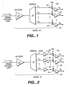
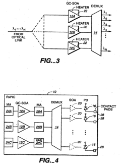
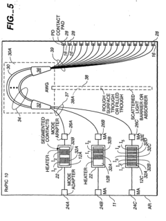
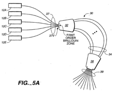
Demultiplexing optical signal receiver photonic integrated circuit
PatentInactiveEP1488265B1
Innovation
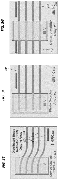
- The implementation of gain-clamped semiconductor optical amplifiers (GC-SOAs) integrated with arrayed waveguide grating (AWG) demultiplexers and photodiodes on a monolithic PIC chip, ensuring equalized intensity of demultiplexed channel signals through on-chip amplification and minimal optical loss, thereby optimizing the responsivity of photodiodes.
Hybrid integration for photonic integrated circuits
PatentActiveUS11340400B2
Innovation
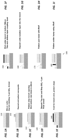
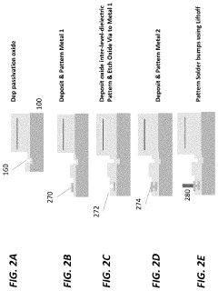
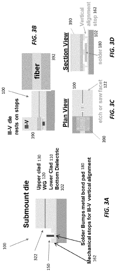
- Hybrid integration techniques that allow coupling of light between silicon PICs and photonic devices from III-V or II-VI materials using silicon oxide claddings, trenches, and pedestals for precise alignment and electrical connection, enabling the integration of light sources, lasers, and optical amplifiers.
Manufacturing Processes and Material Science Considerations
The manufacturing processes for Photonic Integrated Circuits (PICs) and fiber optics represent fundamentally different approaches to light manipulation technologies. PICs typically employ semiconductor fabrication techniques similar to those used in electronic integrated circuits, including photolithography, etching, and deposition processes. Silicon photonics, the most common PIC platform, leverages CMOS-compatible processes that enable high-volume production and potential integration with electronic components. However, these processes require extremely precise control of dimensions at nanometer scales, as optical waveguide geometries directly impact light propagation characteristics.
In contrast, fiber optic manufacturing involves drawing glass preforms into thin strands under carefully controlled temperature conditions. This process, while mature, demands different expertise in materials handling and thermal management. Modern fiber manufacturing can achieve remarkable consistency in core-cladding structures across kilometers of fiber, with specialized techniques for creating complex fiber designs such as photonic crystal fibers or multi-core fibers.
Material considerations for these technologies diverge significantly. PICs primarily utilize silicon-on-insulator (SOI), indium phosphide (InP), silicon nitride, or lithium niobate platforms. Each material system offers distinct advantages: silicon provides cost-effectiveness and electronic integration potential, InP enables efficient light emission, silicon nitride offers lower propagation losses, and lithium niobate excels in high-speed modulation. The selection of materials directly impacts device performance, manufacturing complexity, and cost structures.
Fiber optics predominantly rely on silica glass with precisely controlled dopant profiles to achieve desired refractive index characteristics. Recent advances have expanded material options to include specialized glasses, polymers for flexible applications, and hybrid structures that enhance specific performance parameters. The material purity requirements for fiber optics are extraordinarily stringent, as impurities at parts-per-billion levels can significantly increase signal attenuation over long distances.
Manufacturing yield and scalability present contrasting challenges. PIC fabrication faces issues with process variations that can dramatically affect optical performance, requiring sophisticated testing and quality control measures. The integration density of PICs continues to increase, demanding ever more precise manufacturing tolerances. Fiber optic production, while benefiting from decades of process optimization, faces different challenges in maintaining consistent optical properties during high-speed drawing processes and in the creation of specialty fibers with complex internal structures.
Energy Efficiency and Sustainability Comparison
Energy efficiency represents a critical dimension in comparing Photonic Integrated Circuits (PICs) and traditional fiber optic technologies. PICs demonstrate significant advantages in power consumption, typically requiring only 10-100 fJ per bit compared to discrete optical components that may consume 1-10 pJ per bit. This order-of-magnitude improvement stems from the reduced propagation distances within integrated circuits and the elimination of multiple conversion stages between electrical and optical domains.
The compact nature of PICs contributes substantially to their sustainability profile. With footprints measured in square millimeters rather than square centimeters or meters for equivalent fiber optic systems, PICs enable dramatic reductions in material usage. This miniaturization translates directly to decreased resource consumption during manufacturing and reduced waste at end-of-life disposal.
Thermal management represents another area where PICs offer sustainability advantages. Traditional fiber optic transceivers often require active cooling systems that consume additional power. In contrast, many PIC designs can operate efficiently with passive cooling solutions, further reducing the overall energy footprint of optical communication systems.
Manufacturing processes for PICs have evolved toward greater sustainability. While early fabrication techniques involved toxic chemicals and energy-intensive processes, modern PIC manufacturing increasingly adopts environmentally friendly approaches. Silicon photonics, in particular, leverages existing semiconductor manufacturing infrastructure, benefiting from decades of optimization for resource efficiency.
Lifecycle assessment studies indicate that PIC-based systems typically demonstrate 30-60% lower carbon footprints compared to equivalent fiber optic implementations when considering the entire product lifecycle. This advantage becomes particularly pronounced in high-density data center environments where thousands of optical connections operate simultaneously.
Despite these advantages, fiber optic technology maintains certain sustainability benefits in specific applications. The raw materials for fiber optics—primarily silica—are abundant and relatively environmentally benign. Additionally, deployed fiber infrastructure demonstrates exceptional longevity, with installed cables often functioning reliably for 25+ years with minimal maintenance, reducing replacement frequency and associated environmental impacts.
The energy efficiency gap between these technologies continues to evolve as both undergo continuous improvement. Recent advances in ultra-low-loss waveguides for PICs and reduced-diameter, lower-mass fiber cables represent parallel sustainability innovations that will shape the comparative environmental impact of these technologies in coming years.
Unlock deeper insights with Patsnap Eureka Quick Research — get a full tech report to explore trends and direct your research. Try now!
Generate Your Research Report Instantly with AI Agent
Supercharge your innovation with Patsnap Eureka AI Agent Platform!