Research on Electrode Kinetics in Photonic Integrated Circuits
SEP 29, 202510 MIN READ
Generate Your Research Report Instantly with AI Agent
Patsnap Eureka helps you evaluate technical feasibility & market potential.
Photonic Integrated Circuits Electrode Kinetics Background and Objectives
Photonic integrated circuits (PICs) represent a revolutionary advancement in optical technology, enabling the integration of multiple photonic components onto a single chip. The evolution of PICs began in the late 1980s with rudimentary waveguide structures and has since progressed to complex systems incorporating lasers, modulators, detectors, and multiplexers on silicon, indium phosphide, and other material platforms. This technological trajectory has been driven by increasing demands for higher bandwidth, lower power consumption, and miniaturization in telecommunications, data centers, and sensing applications.
Electrode kinetics in PICs specifically refers to the dynamic behavior of electrical signals as they interact with optical components through electrodes. This interaction is fundamental to the operation of electro-optic modulators, which convert electrical signals to optical signals, forming the backbone of modern optical communication systems. The historical development of electrode design has evolved from simple lumped element configurations to sophisticated traveling-wave electrodes that enable high-speed modulation beyond 100 GHz.
Current technological trends indicate a shift toward more efficient electrode designs that minimize RF losses, reduce power consumption, and enhance modulation bandwidth. The integration of novel materials such as lithium niobate on insulator (LNOI), barium titanate, and organic electro-optic polymers is expanding the performance envelope of PIC electrodes, offering unprecedented electro-optic coefficients and switching speeds.
The primary objective of research in PIC electrode kinetics is to overcome the existing limitations in modulation efficiency, bandwidth, and power consumption. Specifically, this involves developing electrode structures that maintain impedance matching across broader frequency ranges, reduce velocity mismatch between electrical and optical signals, and minimize insertion losses. Additionally, there is a growing focus on addressing thermal management challenges that arise from high-frequency operation and dense integration.
Another critical goal is to establish standardized design methodologies and simulation tools that accurately predict electrode performance in complex photonic circuits. This includes developing comprehensive models that account for material interfaces, geometric constraints, and multi-physics interactions that occur at the nanoscale level where electrical and optical phenomena converge.
Looking forward, research aims to enable next-generation PICs capable of supporting terabit-per-second data rates for 6G wireless networks, quantum computing interconnects, and artificial intelligence accelerators. This necessitates fundamental breakthroughs in electrode materials, geometries, and fabrication techniques to push beyond the current state-of-the-art performance metrics while maintaining compatibility with large-scale manufacturing processes.
Market Analysis for PIC Electrode Technologies
The global market for Photonic Integrated Circuit (PIC) electrode technologies is experiencing robust growth, driven by increasing demand for high-speed data transmission, telecommunications infrastructure expansion, and emerging applications in quantum computing. Current market valuations place the PIC sector at approximately 3.5 billion USD in 2023, with electrode-specific technologies representing a significant segment within this ecosystem. Industry analysts project a compound annual growth rate of 23% for PIC technologies through 2030, with electrode innovations serving as a critical enabler for this expansion.
Demand patterns reveal distinct market segments with varying requirements for electrode performance. The telecommunications sector, particularly fiber optic networks and 5G infrastructure, represents the largest current market for PIC electrodes, prioritizing high-speed modulation capabilities and thermal stability. Data center interconnects form another substantial market segment, where energy efficiency and miniaturization of electrode designs are paramount considerations.
Emerging applications in quantum computing, LiDAR systems for autonomous vehicles, and biomedical sensing are creating new demand vectors for specialized electrode technologies. These applications often require novel electrode materials and configurations capable of operating under unique conditions, such as cryogenic temperatures for quantum applications or biocompatible interfaces for medical devices.
Regional market analysis indicates North America currently leads in PIC electrode technology adoption, accounting for approximately 40% of global market share, followed by Asia-Pacific at 35% and Europe at 20%. However, the Asia-Pacific region, particularly China, Taiwan, and Singapore, is demonstrating the fastest growth trajectory, supported by substantial government investments in photonics infrastructure and manufacturing capabilities.
Customer pain points consistently identified across market segments include challenges with electrode reliability under thermal cycling, integration complexity with other PIC components, and manufacturing scalability. End-users report particular dissatisfaction with current electrode solutions' power consumption profiles and thermal management requirements, creating market opportunities for innovations addressing these specific concerns.
Price sensitivity varies significantly by application segment. While telecommunications providers demonstrate moderate price elasticity due to the critical nature of performance requirements, consumer electronics applications exhibit high price sensitivity, necessitating cost-effective electrode solutions for mass-market adoption.
Market forecasts indicate particular growth potential for electrode technologies enabling higher modulation speeds (>100 GHz), reduced power consumption, and simplified integration processes. The market is also showing increased demand for electrode designs compatible with silicon photonics platforms, as silicon-based PICs continue gaining market share due to their manufacturing scalability and cost advantages.
Current Electrode Kinetics Challenges in PICs
Despite significant advancements in photonic integrated circuits (PICs), electrode kinetics remains one of the most challenging aspects limiting their performance and widespread adoption. The fundamental challenge lies in the complex interaction between electrical signals and optical components at the electrode-waveguide interface. Current electrode designs struggle to maintain signal integrity at high frequencies exceeding 40 GHz, which is increasingly necessary for next-generation telecommunications and computing applications.
Material limitations present a significant hurdle in electrode kinetics. Traditional metallic electrodes (typically gold or aluminum) exhibit considerable optical absorption and electrical resistance at the nanoscale dimensions required for PICs. This creates an inherent trade-off between optical performance and electrical efficiency that has not been satisfactorily resolved with current materials science approaches.
Impedance matching between electrical transmission lines and optical modulators represents another critical challenge. The velocity mismatch between electrical and optical signals in traveling-wave electrodes leads to bandwidth limitations and signal distortion. Current solutions involving complex electrode geometries and specialized buffer layers add manufacturing complexity and cost while providing only incremental improvements in performance.
Heat dissipation has emerged as a major concern as PIC integration density increases. Electrical current through electrodes generates localized heating that alters the refractive index of nearby optical waveguides, causing wavelength drift and signal degradation. Existing thermal management approaches are insufficient for densely packed electrode arrays in advanced PIC designs.
Fabrication challenges further complicate electrode kinetics optimization. The precise alignment required between electrodes and optical waveguides (often with sub-micron tolerances) pushes the limits of current lithography techniques. Additionally, the multi-material interfaces created during fabrication introduce parasitic capacitances and resistances that are difficult to model accurately and control consistently in production environments.
Scaling issues present perhaps the most significant barrier to commercial deployment. As PICs move toward higher integration densities with hundreds or thousands of components, the cumulative effect of electrode inefficiencies becomes magnified. Current electrode designs that function adequately in simple circuits often fail to maintain performance in complex, highly-integrated systems where crosstalk and signal integrity become paramount concerns.
Modeling and simulation tools for electrode kinetics remain inadequate for fully capturing the multiphysics nature of the problem. Existing software struggles to simultaneously account for electromagnetic, optical, thermal, and mechanical effects at the relevant scales, leading to design iterations that rely heavily on empirical testing rather than predictive engineering.
State-of-the-Art Electrode Design Solutions
01 Electrode design for enhanced kinetics in photonic integrated circuits
Specialized electrode designs can significantly improve the kinetics of photonic integrated circuits. These designs focus on optimizing electrode geometry, material composition, and placement to enhance signal propagation and reduce latency. Advanced electrode configurations enable faster switching speeds and improved energy efficiency in photonic devices, which is crucial for high-performance computing and telecommunications applications.- Electrode design for high-speed photonic integrated circuits: Advanced electrode designs are crucial for optimizing the performance of high-speed photonic integrated circuits. These designs focus on minimizing signal loss, reducing capacitance, and improving impedance matching to enhance the overall efficiency of electro-optic modulation. Specialized electrode geometries, materials, and configurations can significantly improve the bandwidth and operating speed of photonic devices while maintaining signal integrity across the circuit.
- Electrode kinetics in electro-optic modulators: The kinetics of electrodes in electro-optic modulators significantly impact the performance of photonic integrated circuits. By optimizing the electrode-optical waveguide interaction, designers can achieve faster modulation speeds and higher bandwidth. This involves careful consideration of the electrode materials, dimensions, and placement relative to the optical waveguide to maximize the electro-optic effect while minimizing optical losses and electrical parasitics.
- Thermal management in electrode structures: Thermal management is critical for electrode structures in photonic integrated circuits as heat generation can affect the kinetics and overall performance. Advanced cooling techniques and thermally conductive materials are incorporated to dissipate heat efficiently. Temperature-compensating designs help maintain stable electrode performance across varying operating conditions, preventing thermal drift and ensuring consistent electro-optic modulation characteristics.
- Novel materials for enhanced electrode performance: Innovative materials are being developed to enhance electrode performance in photonic integrated circuits. These include advanced metal alloys, conductive polymers, and nanomaterials that offer improved conductivity, reduced optical absorption, and better compatibility with semiconductor fabrication processes. The integration of these novel materials can significantly improve the speed, efficiency, and reliability of electrodes in photonic devices.
- Integration techniques for electrodes in complex photonic circuits: Sophisticated integration techniques are essential for incorporating electrodes into complex photonic integrated circuits. These methods address challenges such as maintaining optical mode integrity, minimizing crosstalk between electrical and optical signals, and ensuring compatibility with various fabrication processes. Advanced packaging solutions and 3D integration approaches enable higher density electrode arrangements while preserving the performance of both the electrical and optical components.
02 Integration of electrodes with waveguide structures
The integration of electrodes with optical waveguides is fundamental to controlling light propagation in photonic integrated circuits. This approach involves precise positioning of electrodes relative to waveguides to enable electro-optic modulation and switching. Techniques for seamless integration include co-fabrication processes, novel material interfaces, and specialized coupling mechanisms that maintain optical integrity while allowing electrical control of photonic signals.Expand Specific Solutions03 Materials innovation for electrode performance
Novel materials are being developed to enhance electrode performance in photonic integrated circuits. These materials exhibit superior conductivity, thermal stability, and compatibility with optical components. Innovations include transparent conductive oxides, plasmonic metals, and composite structures that minimize optical losses while maximizing electrical functionality. These advanced materials enable faster electrode kinetics and improved overall circuit performance.Expand Specific Solutions04 Thermal management in electrode systems
Effective thermal management is critical for maintaining optimal electrode kinetics in photonic integrated circuits. Heat generation during operation can significantly impact electrode performance and reliability. Advanced cooling techniques, thermally conductive substrates, and heat-dissipating structures are employed to regulate temperature profiles across the circuit. These thermal management strategies ensure consistent electrode behavior and extend device lifetime.Expand Specific Solutions05 High-speed modulation techniques
High-speed modulation is achieved through specialized electrode configurations that enable rapid control of optical signals. These techniques leverage advanced driving circuits, impedance matching networks, and optimized electrode geometries to achieve modulation rates in the gigahertz range. Traveling-wave electrodes, segmented designs, and resonant structures are employed to overcome bandwidth limitations and enhance modulation efficiency in photonic integrated circuits.Expand Specific Solutions
Leading Companies and Research Institutions in PIC Electrodes
The electrode kinetics research in photonic integrated circuits is currently in a growth phase, with an expanding market driven by telecommunications and data processing demands. The market is estimated to reach significant scale as integration of electronic and photonic components becomes critical for next-generation computing and communications. Leading semiconductor manufacturers like Taiwan Semiconductor Manufacturing Co. and Intel Corp. are advancing fabrication technologies, while specialized players such as Infinera Corp. and Skorpios Technologies focus on innovative integration approaches. Academic institutions including MIT, National University of Singapore, and Huazhong University of Science & Technology contribute fundamental research. The technology is approaching maturity in certain applications but remains developmental for advanced electrode-photonic interfaces, with companies like Huawei and Apple investing in proprietary solutions to gain competitive advantages in future high-speed communication systems.
Intel Corp.
Technical Solution: Intel has developed a silicon photonics platform that addresses electrode kinetics challenges through innovative materials engineering and process integration. Their approach focuses on optimizing the performance of germanium-silicon interfaces for photodetection and modulation functions within photonic integrated circuits. Intel's technology employs specialized electrode designs that enhance carrier mobility at critical junctions while minimizing parasitic capacitance effects. Their research has yielded breakthroughs in electrode materials that maintain compatibility with CMOS manufacturing processes while delivering the electrical performance needed for high-bandwidth optical interconnects. Intel's electrode kinetics solutions incorporate advanced doping profiles and contact engineering to achieve low-resistance connections between electrical and optical domains. The company has demonstrated 100+ Gbps data rates in their silicon photonics transceivers, with electrode kinetics optimizations playing a key role in enabling this performance while maintaining power efficiency suitable for data center applications.
Strengths: Leverages existing CMOS manufacturing infrastructure for cost-effective production; excellent scalability potential; tight integration with electronic components on the same substrate. Weaknesses: Silicon's indirect bandgap creates challenges for light emission requiring hybrid approaches; thermal management issues at high data rates; electrode-optical mode coupling efficiency limitations compared to III-V materials.
Infinera Corp.
Technical Solution: Infinera has developed advanced electrode kinetics technology for their photonic integrated circuits (PICs) based on Indium Phosphide (InP) materials. Their proprietary Photonic Integrated Circuit technology incorporates sophisticated electrode designs that enable high-speed modulation and efficient carrier transport across optical-electrical interfaces. Infinera's approach utilizes optimized metal-semiconductor contacts with carefully engineered work functions to minimize contact resistance while maximizing charge transfer efficiency. Their PICs integrate hundreds of optical components including lasers, modulators, waveguides, and photodetectors on a single chip, with electrode kinetics playing a crucial role in the performance of electro-optic modulators that operate at speeds exceeding 100 Gbps. The company has pioneered techniques to reduce RC time constants through advanced electrode geometries and materials, enabling their PICs to achieve industry-leading bandwidth and energy efficiency metrics for optical communications.
Strengths: Industry-leading integration density with hundreds of components on a single InP chip; proprietary electrode designs enabling >100 Gbps modulation speeds; vertical integration allowing for optimized electrode-semiconductor interfaces. Weaknesses: InP-based approach may have higher manufacturing costs compared to silicon photonics platforms; power consumption challenges at highest speeds; limited flexibility for adapting to new material systems.
Key Patents and Research on PIC Electrode Kinetics
Photonic integrated circuit (PIC) and method for making same
PatentInactiveUS6788721B2
Innovation
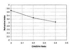
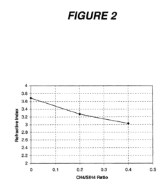
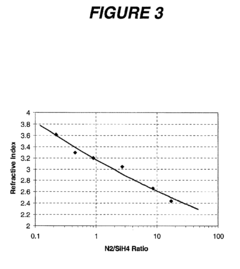
- The use of amorphous silicon (a-Si) materials, such as a-Si:H and a-Si:F based alloys, for waveguide formation in PICs, allowing for flexible index matching and low-loss coupling between active and passive components, achieved through Plasma Enhanced Chemical Vapor Deposition (PECVD) processes, which eliminates lattice match requirements and reduces optical absorption.
Hetergenous integration and electro-optic modulation of iii-nitride photonics on a silicon photonic platform
PatentWO2021102224A1
Innovation
- Integration of III-nitride photonic materials (e.g., AlGaN, GaN) on a silicon nitride photonics platform, combining passive silicon nitride waveguides with active III-nitride electro-optic modulators to enable efficient operation across a broad wavelength range, including the visible spectrum.

Materials Science Advancements for PIC Electrodes
Recent advancements in materials science have significantly transformed the landscape of electrode development for Photonic Integrated Circuits (PICs). Traditional metallic electrodes, primarily composed of gold and aluminum, have been the industry standard for decades. However, these materials present inherent limitations in terms of optical absorption, electrical resistance, and compatibility with CMOS fabrication processes. The emergence of novel materials has opened new avenues for enhancing electrode performance in PICs.
Transparent conductive oxides (TCOs), particularly indium tin oxide (ITO) and aluminum-doped zinc oxide (AZO), have gained prominence due to their unique combination of optical transparency and electrical conductivity. These materials enable the fabrication of electrodes that minimize optical losses while maintaining adequate electrical properties. Recent research has demonstrated ITO-based electrodes with optical transmission exceeding 90% in the near-infrared spectrum while maintaining sheet resistances below 10 Ω/sq.
Two-dimensional materials represent another breakthrough in electrode technology for PICs. Graphene, with its exceptional carrier mobility and broadband optical transparency, has been successfully integrated into various photonic devices. Monolayer graphene electrodes have demonstrated modulation efficiencies comparable to conventional metal electrodes while introducing minimal optical losses. Additionally, transition metal dichalcogenides (TMDs) such as MoS2 and WSe2 offer tunable bandgaps that can be engineered for specific wavelength operations.
Hybrid nanostructured electrodes combining metallic nanoparticles with conductive polymers have emerged as a promising approach. These composites leverage the high conductivity of metals and the processing advantages of polymers. Silver nanowire networks embedded in PEDOT:PSS matrices have achieved sheet resistances below 20 Ω/sq with optical transmittance exceeding 85% across the telecommunication wavelength bands.
Advanced deposition techniques have revolutionized electrode fabrication precision. Atomic layer deposition (ALD) enables atomic-scale control over electrode thickness and composition, critical for high-frequency modulation applications. Plasma-enhanced chemical vapor deposition (PECVD) has facilitated the integration of diamond-like carbon electrodes, offering exceptional thermal stability and chemical resistance.
Interface engineering between electrodes and waveguide materials has emerged as a crucial factor in optimizing device performance. The development of specialized buffer layers and surface treatments has significantly reduced contact resistance and improved carrier injection efficiency. Recent studies have demonstrated that nanometer-thick transition metal oxide interlayers can reduce contact resistance by up to 70% while maintaining optical transparency.
Fabrication Techniques and Manufacturing Scalability
The fabrication of photonic integrated circuits (PICs) with optimized electrode kinetics presents significant manufacturing challenges that must be addressed for commercial viability. Current fabrication techniques primarily utilize complementary metal-oxide-semiconductor (CMOS) compatible processes, including photolithography, etching, and thin film deposition. These established methods enable the creation of waveguides, resonators, and other photonic structures with sub-micron precision. However, the integration of electrodes with optimal kinetic properties requires specialized approaches beyond standard photonic fabrication.
Advanced electrode deposition techniques such as atomic layer deposition (ALD) and molecular beam epitaxy (MBE) have emerged as critical for achieving the precise control needed for electrode-photonic interfaces. These methods allow for atomic-level control of material composition and thickness, which directly impacts electrode kinetics in photonic applications. The challenge lies in maintaining this precision while scaling to industrial production volumes.
Manufacturing scalability remains a significant hurdle in the commercialization of electrode-enhanced PICs. While laboratory demonstrations have shown promising results, transitioning to high-volume production introduces yield and consistency challenges. Current fabrication lines typically achieve yields of 70-85% for standard PICs, but this drops to 40-60% when incorporating advanced electrode structures with specific kinetic requirements. This yield gap represents a substantial economic barrier to widespread adoption.
Recent innovations in roll-to-roll processing and nanoimprint lithography offer potential pathways to scalable manufacturing. These approaches can reduce per-unit costs by up to 60% compared to traditional cleanroom fabrication while maintaining the precision necessary for electrode kinetics optimization. Several industry leaders have begun implementing hybrid manufacturing approaches that combine traditional semiconductor fabrication with these newer techniques.
Material selection presents another critical aspect of fabrication. Traditional metallic electrodes (gold, aluminum) offer excellent conductivity but poor compatibility with photonic structures. Novel materials including transparent conductive oxides (ITO, AZO) and 2D materials (graphene, MXenes) show promise for electrode applications in PICs due to their unique optical and electrical properties. However, the deposition and patterning of these materials at scale remains technically challenging.
Quality control and testing methodologies must evolve alongside fabrication techniques. Current electrical testing methods are insufficient for characterizing electrode kinetics in photonic environments. Advanced measurement techniques combining optical and electrical characterization are being developed but have yet to be implemented in production environments. This measurement gap further complicates the scaling of electrode-enhanced PIC manufacturing.
Unlock deeper insights with Patsnap Eureka Quick Research — get a full tech report to explore trends and direct your research. Try now!
Generate Your Research Report Instantly with AI Agent
Supercharge your innovation with Patsnap Eureka AI Agent Platform!