

Photonic Integrated Circuits: Applications in Quantum Computing
SEP 29, 20259 MIN READ
Generate Your Research Report Instantly with AI Agent
Patsnap Eureka helps you evaluate technical feasibility & market potential.
PIC Evolution and Quantum Computing Goals
Photonic Integrated Circuits (PICs) have evolved significantly over the past decades, transitioning from simple optical components to complex integrated systems capable of performing sophisticated operations. The evolution began in the 1980s with basic waveguide structures and has progressed to today's advanced circuits that integrate multiple optical functions on a single chip. This technological trajectory has been driven by telecommunications needs, but is now expanding into quantum computing applications, representing a convergence of photonics and quantum information science.
The fundamental advantage of PICs in quantum computing stems from photons' inherent quantum properties. Light-based qubits can maintain quantum coherence at room temperature, unlike many material-based quantum systems that require extreme cooling. Additionally, photons naturally exhibit low decoherence rates, making them excellent carriers of quantum information. The integration density achievable with modern photonic fabrication techniques enables the creation of complex quantum circuits with unprecedented scalability potential.
Current technical goals for PICs in quantum computing focus on several critical areas. First is the development of deterministic single-photon sources that can reliably produce indistinguishable photons on demand—a fundamental requirement for photonic quantum computing. Second is the creation of low-loss optical circuits capable of maintaining quantum coherence throughout complex operations. Third is the integration of efficient photon detectors directly on-chip to enable complete quantum processing systems.
The quantum computing community has established specific performance metrics for PIC-based quantum systems. These include achieving quantum advantage demonstrations using at least 50-100 qubits with sufficient fidelity to perform meaningful quantum algorithms. Additionally, error rates must be reduced to levels manageable by quantum error correction techniques, typically requiring physical error rates below 10^-3 per gate operation.
Long-term objectives include scaling photonic quantum processors to thousands of qubits while maintaining quantum coherence. This will require significant advances in integrated photonic manufacturing techniques, particularly in areas of precision, reproducibility, and yield. The ultimate goal is to develop fault-tolerant photonic quantum computers capable of solving problems intractable for classical computers, particularly in areas such as quantum simulation, cryptography, and optimization problems.
The convergence of PICs and quantum computing represents a promising pathway toward practical quantum information processing. Unlike electronic approaches that face fundamental thermal and electromagnetic interference challenges, photonic implementations offer unique advantages in coherence time and operational temperature, potentially enabling more accessible quantum computing systems.
Market Analysis for Quantum PIC Solutions
The quantum computing market is experiencing unprecedented growth, with the global market value projected to reach $1.3 billion by 2023 and expected to grow at a CAGR of 56% through 2028. Within this expanding landscape, Photonic Integrated Circuit (PIC) solutions for quantum computing represent a particularly promising segment, estimated to account for approximately 15% of the overall quantum computing hardware market currently.
Demand for quantum PIC solutions is primarily driven by their unique advantages in maintaining quantum coherence at higher temperatures compared to superconducting qubits, potentially reducing the extreme cooling requirements that have traditionally limited quantum computing scalability. This advantage translates to significant cost reductions in infrastructure and operational expenses, making quantum computing more accessible to a broader range of organizations.
The market for quantum PIC solutions shows distinct regional characteristics. North America leads with approximately 45% market share, bolstered by substantial government funding and strong private investment ecosystems. Europe follows at 30%, with particular strength in academic-industrial partnerships advancing photonic quantum technologies. The Asia-Pacific region, growing at the fastest rate, represents 20% of the market with aggressive national quantum initiatives in China, Japan, and Singapore.
Industry verticals showing the strongest demand for quantum PIC solutions include financial services, pharmaceuticals, materials science, and cybersecurity. Financial institutions are particularly interested in quantum advantage for portfolio optimization and risk assessment, while pharmaceutical companies seek breakthroughs in molecular modeling for drug discovery.
Market adoption faces several challenges, including the current limited qubit count in photonic systems, integration complexities with existing computing infrastructure, and the need for specialized programming expertise. However, the market shows strong positive indicators with venture capital investment in quantum photonics startups exceeding $500 million in 2022 alone.
Customer requirements are evolving rapidly, with enterprise clients increasingly seeking hybrid quantum-classical solutions that can deliver near-term value while positioning for longer-term quantum advantage. This has created a growing market for quantum PIC components that can interface with conventional electronic systems, estimated at $120 million annually and growing at over 40% year-over-year.
The market is further stimulated by government initiatives worldwide, with the EU Quantum Flagship, US National Quantum Initiative, and China's national quantum program collectively allocating billions in funding that partially benefits photonic quantum computing research and commercialization efforts.
PIC Technology Status and Quantum Integration Challenges
Photonic Integrated Circuits (PICs) have emerged as a promising platform for quantum computing applications, yet the current technological landscape presents both significant advancements and formidable challenges. At present, PIC technology has reached a maturity level that enables the integration of hundreds to thousands of optical components on a single chip, primarily using silicon photonics, silicon nitride, and indium phosphide platforms.
The global research community has demonstrated remarkable progress in developing key quantum photonic components, including single-photon sources, quantum gates, and detectors. Silicon photonics, leveraging CMOS compatibility, has achieved integration densities exceeding 5,000 components per chip, while maintaining optical losses below 0.1 dB/cm in optimized waveguides. Indium phosphide platforms excel in active component integration, particularly for on-chip light sources crucial for quantum applications.
Despite these advances, significant technical hurdles remain for quantum computing applications. The primary challenge lies in achieving deterministic single-photon generation with high purity, indistinguishability, and efficiency simultaneously. Current approaches using parametric down-conversion or four-wave mixing produce photons probabilistically, limiting scalability for large-scale quantum computation.
Another critical obstacle is the integration of ultra-low-loss optical circuits with efficient quantum light sources and detectors. Quantum states are extremely fragile, and even minimal optical losses can severely degrade quantum information processing capabilities. Current best-in-class integrated photonic circuits still exhibit losses that are prohibitive for fault-tolerant quantum computing operations.
The geographical distribution of PIC technology development shows concentration in North America, Europe, and East Asia. The United States leads in fundamental research through institutions like NIST and MIT, while the European Quantum Flagship program has established strong collaborative networks across multiple countries. China has made substantial investments in quantum photonics, particularly in quantum communication applications, while Japan excels in specialized materials development for quantum photonic integration.
Temperature stability presents another significant challenge, as quantum operations often require cryogenic conditions, while conventional PICs are designed for room temperature operation. The thermal expansion coefficient mismatch between different materials in hybrid integration approaches creates reliability issues that must be addressed for practical quantum computing implementations.
Fabrication precision requirements for quantum photonic circuits exceed those of classical PICs by orders of magnitude. Current lithography techniques struggle to achieve the sub-nanometer precision needed for quantum interference effects, particularly for path-matched circuits where phase stability is critical.
AI-assisted design tools are emerging to address the complexity of quantum photonic circuit design, though the computational resources required for simulating even modest-sized quantum photonic systems remain substantial, highlighting the need for continued advancement in both fabrication technologies and design methodologies.
Current PIC Architectures for Quantum Applications
01 Integration of optical components on a single chip
Photonic integrated circuits (PICs) involve the integration of multiple optical components such as waveguides, modulators, detectors, and light sources on a single chip. This integration enables compact, high-performance optical systems with reduced size, weight, and power consumption compared to discrete optical components. The integration technology allows for complex optical functionalities while maintaining signal integrity across the chip.- Integration of optical components on photonic integrated circuits: Photonic integrated circuits (PICs) involve the integration of multiple optical components such as waveguides, modulators, detectors, and light sources on a single chip. This integration enables complex optical functionalities while reducing size, power consumption, and cost compared to discrete optical components. Various materials including silicon, indium phosphide, and silicon nitride are used as platforms for these integrated optical systems, allowing for different performance characteristics and applications.
- Waveguide structures and coupling techniques in PICs: Advanced waveguide structures are fundamental to photonic integrated circuits, enabling efficient light propagation and manipulation. These structures include various coupling techniques such as grating couplers, edge couplers, and tapered waveguides that facilitate efficient light transfer between different components or between the PIC and external optical fibers. Specialized waveguide designs can control light propagation characteristics, minimize losses, and enable specific functionalities like wavelength filtering or mode conversion.
- Integration of active and passive components in PICs: Modern photonic integrated circuits combine both active components (lasers, modulators, detectors) and passive components (waveguides, splitters, filters) on the same chip. This heterogeneous integration presents challenges in terms of material compatibility and fabrication processes but enables complete optical systems on a single substrate. Various techniques such as wafer bonding, epitaxial growth, and monolithic integration are employed to achieve this integration, with each approach offering different trade-offs in terms of performance, cost, and manufacturability.
- Packaging and interconnection technologies for PICs: Advanced packaging solutions are critical for photonic integrated circuits to interface with the outside world. These include fiber-to-chip coupling techniques, electrical interconnects, and thermal management solutions. Packaging technologies must address challenges such as alignment precision, environmental stability, and compatibility with existing manufacturing processes. Novel approaches include flip-chip bonding, through-silicon vias, and specialized optical interposers that enable efficient connections between the PIC and other components in a system.
- Applications and specialized PIC designs: Photonic integrated circuits are being developed for diverse applications including telecommunications, data centers, sensing, quantum computing, and biomedical devices. Specialized PIC designs address the unique requirements of each application domain, such as high-speed modulators for communications, low-loss waveguides for sensing, or specialized structures for quantum information processing. These application-specific designs often incorporate novel materials, structures, or integration approaches to optimize performance for particular use cases.
02 Silicon photonics and material platforms
Various material platforms are used for photonic integrated circuits, with silicon photonics being particularly prominent due to its compatibility with CMOS manufacturing processes. Other materials include III-V semiconductors, silicon nitride, lithium niobate, and polymer-based platforms. Each material offers specific advantages for different applications, such as low loss, high-speed modulation, or efficient light emission. Hybrid integration approaches combine different materials to leverage their respective strengths.Expand Specific Solutions03 Optical interconnects and data communication
Photonic integrated circuits enable high-bandwidth optical interconnects for data communication applications. These circuits support high-speed data transmission with reduced power consumption compared to electronic interconnects. PICs incorporate components for wavelength division multiplexing, optical modulation, and photodetection to achieve multi-gigabit or terabit data rates. They are crucial for next-generation data centers, telecommunications, and high-performance computing systems.Expand Specific Solutions04 Integration with electronic circuits
The co-integration of photonic and electronic circuits creates powerful electro-optical systems. These hybrid circuits combine the high-speed data processing capabilities of electronics with the bandwidth advantages of photonics. Various approaches include monolithic integration, 3D stacking, and interposer-based solutions. The electronic components provide control, signal processing, and power management functions while the photonic elements handle optical signal generation, modulation, and detection.Expand Specific Solutions05 Novel photonic circuit architectures and applications
Advanced photonic integrated circuit architectures enable emerging applications beyond traditional telecommunications. These include optical sensing, quantum computing, LiDAR systems, biomedical devices, and neuromorphic computing. Novel circuit designs incorporate resonant structures, photonic crystals, metamaterials, and programmable optical elements. These architectures support functions such as optical signal processing, machine learning acceleration, and specialized sensing applications.Expand Specific Solutions
Leading Companies in Quantum PIC Development
Photonic Integrated Circuits (PICs) in quantum computing are in an early growth phase, with the market expected to expand significantly as quantum technologies mature. Currently, the market size is relatively small but projected to grow rapidly due to increasing investments in quantum computing infrastructure. Leading players include PsiQuantum, which is developing photonic qubits for fault-tolerant quantum computing, and academic powerhouses like MIT and Caltech driving fundamental research. Industry giants such as Intel and TSMC are leveraging their semiconductor expertise to advance PIC manufacturing capabilities. Specialized companies like Rockley Photonics and Shanghai Xizhi Technology are developing innovative photonic chip solutions, while research institutions like CNRS and University of California are contributing to technological breakthroughs. The ecosystem is characterized by strategic collaborations between academia, startups, and established semiconductor manufacturers.
Taiwan Semiconductor Manufacturing Co., Ltd.
Technical Solution: TSMC has developed advanced photonic integrated circuit manufacturing capabilities specifically tailored for quantum computing applications. Their technology leverages their industry-leading semiconductor fabrication processes to create high-performance PICs with exceptional precision and yield. TSMC's quantum photonics platform integrates multiple photonic components including low-loss waveguides, high-efficiency grating couplers, and tunable beam splitters on a single chip. The company has pioneered specialized fabrication techniques to achieve ultra-low waveguide losses below 0.1 dB/cm in their silicon photonic platform, critical for maintaining quantum coherence[7]. TSMC has also developed advanced packaging solutions that enable efficient coupling between photonic chips and optical fibers with coupling losses under 1 dB per connection. Their manufacturing process supports the integration of phase shifters with sub-microsecond switching times and precise phase control better than π/1000, enabling high-fidelity quantum operations. TSMC's photonic foundry services now include specialized process design kits for quantum photonic applications, allowing quantum computing researchers and companies to fabricate custom designs with predictable performance characteristics[8].
Strengths: Unparalleled manufacturing expertise and quality control; ability to produce photonic circuits at scale with high yield; advanced process technologies enabling integration of multiple photonic and electronic components. Weaknesses: Primary focus on manufacturing rather than quantum algorithm implementation; requires partnerships with quantum computing specialists to develop complete systems; current processes still being optimized specifically for quantum photonic requirements.
PsiQuantum Corp.
Technical Solution: PsiQuantum has developed a unique approach to quantum computing using photonic integrated circuits (PICs). Their technology leverages silicon photonics to build fault-tolerant quantum computers with millions of qubits. The company's architecture uses photons as quantum bits, which naturally maintain quantum coherence at room temperature and can be manipulated using standard integrated photonic components. PsiQuantum has partnered with GlobalFoundries to manufacture their quantum photonic chips using conventional semiconductor fabrication techniques[1]. Their approach integrates single-photon sources, detectors, and linear optical components on a single chip, enabling complex quantum operations through optical interference. The company has developed specialized error correction protocols specifically designed for photonic quantum computing systems, addressing the unique challenges of photon loss and detection inefficiencies[2].
Strengths: Scalability through established semiconductor manufacturing processes; room temperature operation without requiring extreme cooling; inherent compatibility with fiber optic networks for quantum communication. Weaknesses: Challenges in achieving high-efficiency single-photon sources and detectors; requires complex error correction due to probabilistic nature of some photonic quantum gates; higher overhead for certain quantum operations compared to superconducting approaches.
Key Patents in Quantum Photonic Integration
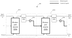
Time bin qubit converter
PatentWO2024054261A2
Innovation
- A system comprising a first photonic integrated circuit with a qubit encoder that converts spatial-mode qubits to temporal-mode qubits using an optical delay and switch, and a second photonic integrated circuit with a qubit decoder that converts them back, utilizing a dual-rail qubit bus with waveguide delay lines and optical switches synchronized with a clock signal.

Quantum PIC Fabrication Techniques
The fabrication of Quantum Photonic Integrated Circuits (QPICs) represents one of the most challenging aspects in the development of quantum computing platforms. Current fabrication techniques have evolved from traditional photonic integration methods but require significantly higher precision and lower loss characteristics to maintain quantum coherence.
Silicon photonics has emerged as a leading platform for QPIC fabrication due to its compatibility with CMOS manufacturing processes. The 220nm SOI (Silicon-On-Insulator) platform allows for the creation of low-loss waveguides with propagation losses as low as 0.1 dB/cm. Advanced lithography techniques, including deep-UV and electron-beam lithography, enable feature sizes below 100nm, critical for creating structures that can manipulate single photons effectively.
Thin-film lithium niobate (TFLN) has gained significant attention as an alternative material platform. TFLN offers exceptional electro-optic properties with modulation bandwidths exceeding 100 GHz and lower optical losses compared to bulk lithium niobate. The plasma-enhanced chemical vapor deposition (PECVD) technique has been refined to create high-quality TFLN films with thicknesses controlled to within a few nanometers.
For quantum applications requiring non-classical light sources, III-V semiconductor integration has proven valuable. Techniques such as wafer bonding and epitaxial growth allow for the integration of quantum dot single-photon sources with silicon photonic circuits. Recent advances in heterogeneous integration have reduced the coupling losses between disparate material platforms to below 1 dB per interface.
Precision doping techniques have been developed to create on-chip single-photon detectors, particularly using superconducting nanowire single-photon detectors (SNSPDs). These require specialized thin-film deposition of materials like niobium nitride or tungsten silicide with thickness control at the nanometer scale, followed by electron-beam lithography to define nanowires with widths as narrow as 50nm.
Multi-layer fabrication processes have become essential for creating 3D photonic circuits that enable more complex quantum operations. Techniques such as chemical-mechanical polishing (CMP) and wafer bonding allow for the vertical integration of multiple photonic layers with precise alignment between layers (typically <100nm misalignment).
Packaging remains a significant challenge, with fiber-to-chip coupling requiring specialized grating couplers or edge couplers to achieve coupling efficiencies exceeding 90%. Cryogenic packaging solutions have been developed to interface QPICs with superconducting control electronics while maintaining thermal isolation and mechanical stability at temperatures below 4 Kelvin.
Standardization Efforts in Quantum PICs
The standardization of Quantum Photonic Integrated Circuits (QPICs) represents a critical frontier in the maturation of quantum computing technologies. Currently, several international bodies are actively developing frameworks to establish common protocols, interfaces, and performance metrics for QPICs. The IEEE Quantum Computing Standards Working Group has initiated specific task forces focused on standardizing quantum photonic components, with particular emphasis on defining standard specifications for single-photon sources, detectors, and waveguide interfaces.
In parallel, the International Electrotechnical Commission (IEC) has formed dedicated technical committees addressing quantum technology standardization, including Working Group 14 which specifically targets photonic integration for quantum applications. These efforts aim to create universally accepted testing methodologies for characterizing quantum photonic devices, ensuring reliability and reproducibility across different manufacturing platforms.
Industry consortia are also making significant contributions to standardization. The Quantum Economic Development Consortium (QED-C) has established a Photonics Technical Advisory Committee that brings together industry leaders to develop best practices for QPIC fabrication and testing. Similarly, the European Quantum Industry Consortium (QuIC) has launched initiatives to harmonize QPIC specifications across European research institutions and commercial entities.
A key focus area in current standardization efforts is the development of standard interfaces between classical electronic control systems and quantum photonic components. The AIM Photonics consortium, in collaboration with NIST, has proposed preliminary specifications for electronic-photonic interfaces specifically designed for quantum applications, addressing challenges in timing synchronization and signal integrity that are crucial for quantum operations.
Material standardization represents another critical domain, with organizations like SEMI developing standards for materials used in quantum photonic fabrication. These standards address the unique requirements of quantum coherence preservation in materials used for waveguides, resonators, and other photonic structures.
Interoperability standards are emerging to ensure that QPICs from different manufacturers can work together in larger quantum computing systems. The OpenQASM initiative has expanded to include specific extensions for photonic quantum computing, allowing for hardware-agnostic programming of quantum photonic devices regardless of their underlying implementation details.
These standardization efforts collectively aim to accelerate the commercialization of quantum photonic technologies by reducing development costs, enabling supply chain diversification, and facilitating system integration across the quantum computing ecosystem. As these standards mature, they will likely serve as catalysts for broader adoption of photonic approaches to quantum information processing.
Unlock deeper insights with Patsnap Eureka Quick Research — get a full tech report to explore trends and direct your research. Try now!
Generate Your Research Report Instantly with AI Agent
Supercharge your innovation with Patsnap Eureka AI Agent Platform!