Thermal Management Techniques for Photonic Integrated Circuits
SEP 29, 20259 MIN READ
Generate Your Research Report Instantly with AI Agent
Patsnap Eureka helps you evaluate technical feasibility & market potential.
PIC Thermal Management Background and Objectives
Photonic Integrated Circuits (PICs) have emerged as a transformative technology in the field of optoelectronics, enabling the integration of multiple optical components onto a single chip. The evolution of PICs began in the late 1980s, with significant advancements occurring in the 2000s as fabrication techniques improved. However, as integration density increases, thermal management has become a critical challenge that threatens to impede further progress in this field.
Thermal issues in PICs arise primarily from active components such as lasers, modulators, and detectors that generate heat during operation. Unlike electronic integrated circuits, PICs are particularly sensitive to temperature variations, as optical properties including refractive index, absorption coefficients, and bandgap energies are temperature-dependent. Even small temperature fluctuations can cause wavelength shifts, bandwidth reduction, and overall performance degradation.
The historical trajectory of thermal management in PICs has evolved from simple passive cooling techniques to more sophisticated approaches. Early solutions focused on substrate material selection and basic heat sinking, while current research explores advanced materials, active cooling systems, and novel architectural designs that distribute heat-generating components more effectively across the chip.
Industry trends indicate a growing demand for higher integration density and increased functionality in PICs, particularly for applications in telecommunications, data centers, sensing, and quantum computing. This push toward miniaturization and enhanced performance intensifies thermal challenges, making effective thermal management a key enabler for next-generation photonic technologies.
The primary technical objectives for PIC thermal management include developing solutions that can maintain temperature uniformity across the chip, efficiently dissipate heat from active components, minimize thermal crosstalk between adjacent elements, and achieve these goals without significantly increasing manufacturing complexity or cost. Additionally, thermal management techniques must be compatible with existing fabrication processes and scalable for mass production.
Recent research has begun exploring biomimetic approaches, phase-change materials, and three-dimensional integration techniques to address thermal challenges. The convergence of nanotechnology and photonics also offers promising avenues for innovative thermal management solutions, such as phononic crystals and metamaterials engineered specifically for heat manipulation at the nanoscale.
As the field advances, the ultimate goal is to develop thermal management techniques that not only solve current challenges but anticipate future needs as PIC technology continues to evolve toward higher integration densities, novel materials, and more diverse application domains. This requires a holistic approach that considers thermal effects from the earliest stages of design through to final implementation and operation.
Market Demand Analysis for Thermally Efficient PICs
The global market for thermally efficient Photonic Integrated Circuits (PICs) is experiencing robust growth, driven by increasing data traffic demands and the expansion of optical communication networks. Current market analysis indicates that the PIC market is projected to grow at a compound annual growth rate of 23% through 2028, with thermal management solutions representing a critical segment of this expansion.
Telecommunications remains the primary driver for thermally efficient PICs, accounting for approximately 40% of market demand. As 5G networks continue to deploy globally and 6G research accelerates, the need for high-performance, thermally stable optical components has become paramount. Network operators are specifically seeking PICs that can maintain consistent performance under varying thermal conditions while supporting higher data rates.
Data center applications represent the fastest-growing segment for thermally efficient PICs, with demand increasing by 30% annually. The shift toward optical interconnects within data centers has intensified requirements for PICs that can operate reliably in dense computing environments where heat dissipation presents significant challenges. Major cloud service providers are actively investing in thermally optimized photonic solutions to reduce cooling costs and improve energy efficiency metrics.
Consumer electronics applications are emerging as a significant market opportunity, particularly in augmented reality/virtual reality (AR/VR) devices and advanced sensing systems. These applications demand miniaturized PICs with excellent thermal stability to ensure consistent performance in variable ambient conditions and confined spaces. The consumer segment is expected to grow substantially as photonic components become more integrated into everyday devices.
Regional analysis reveals that North America currently leads the market for thermally efficient PICs, followed closely by Asia-Pacific. However, the Asia-Pacific region is demonstrating the highest growth rate, fueled by extensive investments in optical communication infrastructure across China, Japan, and South Korea. European markets show steady growth, supported by research initiatives focused on sustainable photonic technologies.
End-user surveys indicate that thermal management capabilities now rank among the top three purchasing criteria for PIC solutions, alongside performance specifications and cost considerations. This represents a significant shift from five years ago when thermal characteristics were often secondary considerations in procurement decisions.
Industry stakeholders are increasingly willing to pay premium prices for PICs with superior thermal management features, recognizing the long-term operational benefits and reliability improvements. This price elasticity has created market opportunities for specialized thermal management solutions that can command 15-25% higher prices compared to standard offerings while delivering demonstrable improvements in system-level performance and energy efficiency.
Current Thermal Management Challenges in Photonics
Photonic integrated circuits (PICs) face significant thermal management challenges that impede their performance, reliability, and integration density. As these devices continue to miniaturize while handling increasing optical power densities, heat dissipation has emerged as a critical bottleneck in their development trajectory. Current PICs typically experience temperature gradients of 20-50°C across the chip during operation, severely affecting wavelength stability and optical coupling efficiency.
The fundamental challenge stems from the inherent thermal sensitivity of photonic components. Waveguides, resonators, and modulators exhibit temperature-dependent refractive indices, with typical thermal-optic coefficients ranging from 10^-5 to 10^-4 K^-1. This translates to wavelength shifts of approximately 0.1nm/°C in silicon photonics, which can completely disrupt device functionality in wavelength-critical applications like WDM systems.
Material interfaces present another significant thermal management hurdle. The thermal boundary resistance between dissimilar materials in multilayer PIC structures creates barriers to efficient heat transfer. For instance, the thermal conductivity mismatch between silicon (149 W/m·K) and silicon dioxide (1.4 W/m·K) creates substantial thermal bottlenecks in SOI-based photonic platforms. These interface effects become increasingly problematic as device dimensions shrink below the micron scale.
Active photonic components such as lasers, semiconductor optical amplifiers, and electro-optic modulators generate substantial heat during operation. In particular, heterogeneously integrated III-V lasers on silicon can generate heat fluxes exceeding 10^4 W/cm², concentrated in extremely small active regions. This localized heating creates hotspots that can lead to thermal runaway effects and catastrophic device failure if not properly managed.
The integration of electronics with photonics in emerging electro-photonic integrated circuits (EPICs) compounds these thermal challenges. Electronic components typically operate optimally at lower temperatures than their photonic counterparts, creating conflicting thermal management requirements within the same package. Current thermal solutions often compromise either electronic or photonic performance.
Packaging constraints further exacerbate thermal management difficulties. As PICs move toward 3D integration and higher density packaging, thermal pathways become increasingly restricted. Traditional heat sinking approaches that work for electronic ICs often prove inadequate for photonic components due to optical access requirements and the need to maintain precise alignment between optical components.
Measurement and modeling of thermal effects in PICs remain challenging due to the complex interplay between electrical, optical, and thermal phenomena. Current simulation tools often fail to accurately capture the multiphysics nature of heat generation and dissipation in photonic devices, leading to suboptimal thermal management strategies and unexpected thermal behaviors in fabricated devices.
Current Thermal Dissipation Approaches for PICs
01 Heat dissipation structures for photonic integrated circuits
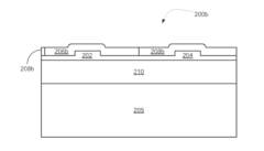
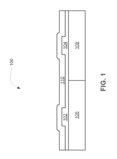
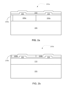
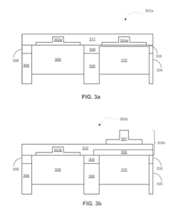
Various heat dissipation structures can be integrated with photonic integrated circuits to manage thermal issues. These include heat sinks, thermal vias, and specialized thermal conductive layers that efficiently transfer heat away from critical optical components. These structures are designed to maintain optimal operating temperatures and prevent performance degradation due to thermal effects in high-density photonic circuits.- Heat dissipation structures for photonic integrated circuits: Various heat dissipation structures can be integrated with photonic integrated circuits to manage thermal issues. These include heat sinks, thermal vias, and specialized thermal conductive layers that efficiently transfer heat away from critical optical components. These structures are designed to maintain optimal operating temperatures and prevent performance degradation due to thermal effects in high-density photonic circuits.
- Active cooling techniques for photonic integrated circuits: Active cooling methods are employed to manage thermal issues in photonic integrated circuits, including thermoelectric coolers, microfluidic cooling channels, and active temperature control systems. These techniques provide dynamic thermal management capabilities that can respond to changing operational conditions and heat loads, maintaining optimal performance of temperature-sensitive photonic components.
- Thermally optimized materials and substrates: Specialized materials and substrates with enhanced thermal conductivity properties are used in photonic integrated circuits to improve heat dissipation. These include thermally conductive polymers, ceramic substrates, and composite materials designed to efficiently spread and dissipate heat while maintaining optical performance. The selection of appropriate materials plays a crucial role in passive thermal management strategies.
- Thermal isolation techniques for temperature-sensitive components: Thermal isolation strategies are implemented to protect temperature-sensitive photonic components from heat sources within the circuit. These include creating thermal barriers, using isolation trenches, implementing suspended structures, and designing thermal breaks in the circuit layout. These techniques help maintain stable operating conditions for critical components like lasers, modulators, and detectors that require precise temperature control.
- Integrated thermal monitoring and control systems: Advanced photonic integrated circuits incorporate on-chip thermal sensors and control systems that continuously monitor temperature distributions and actively manage thermal conditions. These systems can include distributed temperature sensors, feedback control loops, and adaptive thermal management algorithms that optimize performance while preventing thermal damage. This approach enables real-time thermal management across the entire photonic circuit.
02 Active cooling techniques for photonic integrated circuits
Active cooling methods provide dynamic thermal management for photonic integrated circuits. These techniques include thermoelectric coolers, microfluidic cooling channels, and active temperature control systems that can adjust cooling capacity based on operational demands. Active cooling is particularly important for temperature-sensitive photonic components that require precise thermal control to maintain wavelength stability and optical performance.Expand Specific Solutions03 Thermally optimized packaging for photonic integrated circuits
Specialized packaging designs can significantly improve thermal management in photonic integrated circuits. These include thermally conductive encapsulation materials, optimized substrate designs with improved thermal conductivity, and packaging architectures that facilitate efficient heat flow. The packaging approaches focus on creating thermal paths that direct heat away from sensitive optical components while maintaining mechanical stability and optical alignment.Expand Specific Solutions04 Thermal isolation techniques for temperature-sensitive components
Thermal isolation strategies protect temperature-sensitive photonic components from heat generated by other circuit elements. These include creating thermal barriers, implementing isolation trenches, using materials with low thermal conductivity as buffers, and designing circuit layouts that physically separate heat-generating components from temperature-sensitive optical elements. These approaches help maintain stable operating conditions for critical photonic components.Expand Specific Solutions05 Integrated thermal sensors and feedback control systems
Incorporating thermal sensors directly into photonic integrated circuits enables real-time temperature monitoring and adaptive thermal management. These systems include on-chip temperature sensors, feedback control mechanisms, and intelligent thermal management algorithms that can dynamically adjust operating parameters or cooling responses based on thermal conditions. This approach allows for precise temperature control and helps prevent thermal-induced performance degradation in complex photonic systems.Expand Specific Solutions
Key Industry Players in Photonic Thermal Management
Thermal Management for Photonic Integrated Circuits is currently in a growth phase, with the market expanding as photonic integration becomes critical for data centers and telecommunications. The global market is projected to reach significant scale as thermal issues become limiting factors in PIC performance. Technology maturity varies across players: Intel, IBM, and TSMC lead with advanced cooling solutions; Huawei and Nokia are developing telecom-specific approaches; while specialized firms like Applied Optoelectronics and FormFactor focus on niche thermal management technologies. Academic-industry partnerships, particularly involving MIT and Huazhong University, are accelerating innovation in this space, with emerging techniques including microfluidic cooling and thermally-optimized materials gaining traction.
Intel Corp.
Technical Solution: Intel has developed advanced thermal management solutions for photonic integrated circuits (PICs) through their Silicon Photonics platform. Their approach includes integrated micro-thermoelectric coolers (μTECs) directly fabricated on silicon photonic chips, providing localized cooling to temperature-sensitive components. Intel's thermal management architecture employs a hierarchical cooling strategy with on-chip thermal sensors for real-time monitoring and feedback control. They've implemented specialized heat spreading layers using materials with high thermal conductivity like diamond-like carbon films to efficiently dissipate heat from active photonic components. Intel has also pioneered 3D integration techniques that incorporate dedicated thermal vias and thermal interposers to manage heat flow between stacked photonic and electronic layers, enabling higher integration density while maintaining thermal stability.
Strengths: Industry-leading integration of cooling solutions directly into manufacturing process; comprehensive thermal design ecosystem that spans from chip to package level; extensive manufacturing capabilities for volume production. Weaknesses: Higher implementation costs compared to passive solutions; increased power consumption for active cooling components; added design complexity requiring specialized expertise.
Huawei Technologies Co., Ltd.
Technical Solution: Huawei has developed a comprehensive thermal management approach for their photonic integrated circuits focusing on both active and passive cooling technologies. Their solution incorporates phase-change materials (PCMs) embedded within the PIC packaging that absorb heat during operation peaks and release it during low-activity periods, effectively dampening thermal fluctuations. Huawei's thermal management system utilizes advanced computational fluid dynamics modeling to optimize heat sink designs specifically for their optical transceivers and network equipment. They've implemented micro-channel liquid cooling directly integrated with silicon photonics platforms, allowing for more efficient heat removal from high-power-density regions. Their approach also includes thermally-aware circuit layout techniques that strategically position heat-generating components to minimize thermal crosstalk between sensitive photonic elements.
Strengths: Holistic approach combining materials science, packaging innovation, and system-level thermal management; strong integration with their telecommunications equipment ecosystem; proven deployment in real-world high-density networking environments. Weaknesses: Proprietary solutions may limit broader industry adoption; liquid cooling approaches increase complexity and potential reliability concerns; higher manufacturing costs compared to conventional cooling methods.
Critical Patents in PIC Thermal Management
Thermal management for photonic integrated circuits
PatentActiveUS20170205577A1
Innovation
- The implementation of locally tailored high and low thermal impedance regions on PICs, achieved through the use of materials like silicon nitride and diamond with similar refractive indices but different thermal conductivities, allows for improved heat dissipation and thermal isolation without affecting optical performance.
Integrated circuit
PatentWO2015059226A1
Innovation
- A heterogeneous photonic integrated device with a micro-thermoelectric module integrally formed next to temperature-sensitive semiconductor components, allowing for efficient temperature control by reducing thermal resistance and eliminating the need for separate cooling and heating components, thereby optimizing thermal management.
Materials Science Advancements for Thermal Conductivity
Recent advancements in materials science have significantly contributed to improving thermal management in Photonic Integrated Circuits (PICs). Traditional semiconductor materials like silicon and indium phosphide, while excellent for optical functionality, often present thermal conductivity limitations that hinder heat dissipation in densely packed photonic circuits.
Novel composite materials incorporating diamond particles have emerged as promising solutions for enhanced thermal conductivity. Chemical Vapor Deposition (CVD) diamond films, with thermal conductivity values exceeding 2000 W/mK, represent a five-fold improvement over conventional silicon substrates. These materials can be strategically integrated as heat spreading layers without compromising the optical performance of PICs.
Two-dimensional materials such as graphene and hexagonal boron nitride (h-BN) have demonstrated exceptional in-plane thermal conductivity values reaching 5000 W/mK and 2000 W/mK respectively. Their atomic thinness allows for integration as thermal interface materials between active photonic components and heat sinks, significantly reducing thermal boundary resistance that typically impedes heat transfer across material interfaces.
Metal-matrix composites incorporating copper or aluminum with ceramic reinforcements have been engineered specifically for PIC applications. These materials offer customizable thermal expansion coefficients that can be matched to photonic substrates, minimizing thermomechanical stress while maintaining thermal conductivity values between 200-500 W/mK, substantially higher than standard packaging materials.
Phase-change materials (PCMs) represent another innovative approach, absorbing excess heat through solid-liquid phase transitions. Advanced PCMs with nanoparticle enhancement have demonstrated heat absorption capacities exceeding 200 J/g, providing effective thermal buffering during transient temperature spikes in high-power photonic operations.
Aerogel-based thermal insulators with engineered thermal conductivity gradients enable precise thermal channeling within PICs. These materials create controlled heat flow pathways, directing heat away from temperature-sensitive components while maintaining thermal isolation between adjacent photonic elements operating at different temperature requirements.
Conformal thermal interface materials utilizing liquid metal alloys (primarily gallium-based) have achieved thermal interface resistances below 5 mm²K/W, representing a significant advancement over conventional thermal greases. These materials ensure maximum thermal contact between photonic chips and cooling systems, eliminating microscopic air gaps that traditionally impede efficient heat transfer.
Integration Strategies with Electronic Cooling Systems
The integration of photonic integrated circuits (PICs) with electronic cooling systems represents a critical frontier in thermal management strategies. As PICs continue to advance in complexity and power density, leveraging existing electronic cooling technologies offers significant advantages for comprehensive thermal solutions. This integration approach enables synergistic thermal management across both electronic and photonic components within the same package.
Traditional electronic cooling systems, including heat sinks, fans, and liquid cooling solutions, can be adapted for PIC applications with appropriate modifications. The key challenge lies in addressing the unique thermal characteristics of photonic components while maintaining compatibility with electronic cooling infrastructure. Thermal interface materials (TIMs) specifically designed for optical-electronic interfaces play a crucial role in this integration, requiring both high thermal conductivity and optical transparency in relevant regions.
Co-designed thermal management systems that simultaneously address both electronic and photonic components demonstrate superior performance compared to isolated approaches. These integrated solutions typically incorporate shared cooling paths, unified thermal spreaders, and common heat sinks that efficiently extract heat from both component types. Recent research indicates that such co-designed systems can reduce overall thermal resistance by 15-30% compared to separate cooling mechanisms.
Thermoelectric coolers (TECs) represent a particularly promising integration strategy, as they can provide localized cooling for temperature-sensitive photonic components while being controlled by the same electronic systems managing the overall thermal environment. Advanced integration approaches incorporate embedded microfluidic channels that service both electronic and photonic regions, with carefully designed flow patterns that prioritize cooling for thermally critical areas.
3D integration techniques further enhance cooling system integration by enabling vertical stacking of cooling layers between electronic and photonic components. This approach maximizes cooling efficiency while minimizing the overall footprint of the integrated system. Thermal vias and through-silicon vias (TSVs) serve as critical thermal conduits in these 3D-integrated structures, facilitating heat transfer between layers.
Industry standards for thermal management integration are emerging, with organizations like JEDEC and IEEE developing specifications for combined electronic-photonic thermal solutions. These standards address thermal interface requirements, testing methodologies, and reliability metrics specific to integrated cooling systems. The development of unified simulation tools that accurately model both electronic and photonic thermal behaviors represents another important advancement in this field, enabling more effective co-design processes.
Unlock deeper insights with Patsnap Eureka Quick Research — get a full tech report to explore trends and direct your research. Try now!
Generate Your Research Report Instantly with AI Agent
Supercharge your innovation with Patsnap Eureka AI Agent Platform!