The Evolution of Photonic Integrated Circuits in Space Exploration
SEP 29, 20259 MIN READ
Generate Your Research Report Instantly with AI Agent
Patsnap Eureka helps you evaluate technical feasibility & market potential.
Photonic IC Evolution and Space Exploration Objectives
Photonic Integrated Circuits (PICs) represent a revolutionary technology that integrates multiple photonic functions on a single chip, similar to electronic integrated circuits but utilizing light instead of electrons. The evolution of PICs has been marked by significant milestones since their conceptualization in the 1960s, with practical implementations emerging in the 1980s and accelerating development in the 2000s as fabrication techniques matured.
In space exploration, PICs offer transformative capabilities due to their inherent advantages of reduced size, weight, and power consumption (SWaP) - critical parameters for space missions where every gram and watt matters. The historical trajectory shows a transition from bulky optical components to increasingly miniaturized and integrated photonic systems capable of withstanding the harsh conditions of space.
The technological evolution has been driven by several key factors: advancements in material science, particularly silicon photonics and III-V compound semiconductors; improvements in fabrication techniques enabling nanometer-scale precision; and the development of hybrid integration approaches combining different material platforms. These advancements have collectively pushed PICs toward higher levels of integration, functionality, and reliability.
Current space exploration objectives heavily influence PIC development trajectories. NASA, ESA, CNSA, and other space agencies are increasingly focusing on deep space missions, extended lunar presence, Mars exploration, and asteroid mining - all requiring sophisticated communication, sensing, and computing capabilities that PICs can potentially provide. Commercial space companies like SpaceX and Blue Origin are similarly driving demand for advanced space-based technologies.
The primary technical objectives for PICs in space applications include radiation hardening to withstand the intense radiation environment beyond Earth's magnetosphere; thermal stability to function across extreme temperature variations; enhanced reliability for long-duration missions where repairs are impossible; and increased integration density to maximize functionality while minimizing payload mass.
Looking forward, the convergence of PICs with quantum technologies presents particularly promising avenues for space exploration. Quantum communication using entangled photons could enable secure communications across vast distances, while quantum sensing could provide unprecedented measurement precision for navigation and scientific instruments.
The roadmap for PIC evolution in space applications envisions progressive integration of increasingly complex photonic systems, transitioning from current discrete components to fully integrated photonic systems-on-chip that combine sensing, communication, and computing functions. This evolution aims to enable autonomous spacecraft with enhanced capabilities for deep space exploration, interplanetary communications, and potentially even interstellar missions in the distant future.
Market Analysis for Space-Grade Photonic ICs
The space-grade photonic integrated circuits (PICs) market is experiencing significant growth driven by the increasing demand for high-performance, radiation-resistant communication systems in space applications. Current market valuations estimate the space-grade PIC sector at approximately $320 million in 2023, with projections indicating a compound annual growth rate of 17.8% through 2030, potentially reaching $1.1 billion by the end of the decade.
This robust growth trajectory is primarily fueled by the expansion of satellite constellations for global internet coverage, with companies like SpaceX's Starlink, Amazon's Project Kuiper, and OneWeb deploying thousands of satellites requiring advanced optical communication systems. The market demand is further strengthened by governmental space agencies' increasing investments in deep space exploration missions, which require reliable, high-bandwidth communication technologies capable of operating in extreme environments.
Market segmentation reveals that laser communication terminals represent the largest application segment, accounting for approximately 42% of the total space-grade PIC market. This is followed by optical sensors and quantum communication devices at 28% and 18% respectively. Geographically, North America dominates with 45% market share, followed by Europe (30%) and Asia-Pacific (20%), with the latter showing the fastest growth rate at 22% annually.
Customer requirements are evolving toward smaller form factors, lower power consumption, and higher radiation tolerance. Space-grade PICs that can withstand total ionizing doses exceeding 100 krad while maintaining operational integrity are in particularly high demand. Additionally, there is growing interest in PICs capable of supporting wavelength division multiplexing with data rates exceeding 100 Gbps for inter-satellite links.
The market faces several constraints, including high development costs, lengthy qualification processes for space-grade components, and limited manufacturing capabilities for radiation-hardened photonic devices. The average development cycle for space-qualified PICs currently stands at 3-4 years, significantly longer than their commercial counterparts.
Emerging trends include the integration of artificial intelligence processors with PICs for on-board data processing, the development of reconfigurable optical add-drop multiplexers for flexible communication networks in space, and the adoption of silicon photonics platforms modified for radiation resistance. Additionally, there is growing interest in quantum-secure communication systems based on entangled photon sources integrated into PICs for satellite-based quantum key distribution networks.
The competitive landscape features established aerospace contractors like Northrop Grumman and Lockheed Martin alongside specialized photonics companies such as Infinera and NeoPhotonics, with recent market entries from startups developing radiation-hardened silicon photonics platforms specifically for space applications.
Current State and Challenges of PICs in Space Applications
Photonic Integrated Circuits (PICs) have emerged as a transformative technology in space exploration, yet their current implementation faces significant challenges. As of 2023, PICs in space applications have reached a moderate level of technological readiness, with several successful demonstrations on satellite platforms and the International Space Station. These implementations primarily focus on optical communication systems, quantum key distribution, and limited sensing applications.
The miniaturization advantages of PICs have proven particularly valuable in the space sector, where payload weight and volume constraints are critical. Current PIC technologies deployed in space typically achieve 10-100 times reduction in size and weight compared to discrete optical components, while consuming 30-50% less power—a crucial benefit for power-limited space systems.
Despite these advancements, significant technical challenges persist. Radiation hardening remains a primary concern, as space radiation can cause performance degradation through ionizing damage to waveguides and active components. Current radiation-hardened PICs demonstrate limited functionality compared to their terrestrial counterparts, with approximately 30-40% fewer integrated components and reduced performance metrics.
Thermal management presents another substantial challenge. The extreme temperature fluctuations in space environments (ranging from -170°C to +120°C in low Earth orbit) can cause misalignment, material stress, and performance drift in PICs. Current thermal compensation techniques add complexity and reduce the integration density advantages of photonic circuits.
Manufacturing reliability and yield issues further complicate space deployment. The space industry requires components with exceptionally high reliability, yet current PIC fabrication processes typically achieve yields below 80% for complex circuits, insufficient for mission-critical applications. This limitation has restricted the complexity of PICs deployed in space missions.
The global distribution of space-qualified PIC technology remains highly concentrated, with primary development centers in the United States, Europe (particularly France and Germany), and increasingly in China. This geographical concentration creates potential supply chain vulnerabilities for space agencies and commercial entities.
Integration challenges with existing spacecraft systems also persist. Current PICs often require specialized interfaces and control electronics that are not standardized across the industry, limiting their plug-and-play capability. The lack of standardized testing protocols for space-qualified PICs further complicates their adoption in mission-critical systems.
Recent technological breakthroughs, such as silicon nitride platforms with enhanced radiation resistance and hybrid integration approaches combining multiple material systems, show promise in addressing these challenges. However, these solutions remain at relatively low Technology Readiness Levels (TRLs 3-5) and require further development before widespread deployment in space missions.
Existing PIC Solutions for Space Environment
01 Integration of optical components on a single chip
Photonic integrated circuits (PICs) involve the integration of multiple optical components such as waveguides, modulators, detectors, and light sources on a single substrate. This integration enables miniaturization of optical systems, reduces power consumption, and improves reliability by eliminating the need for multiple discrete components. The technology allows for complex optical functionalities to be performed within a compact footprint, making it suitable for high-bandwidth communications and data processing applications.- Integration of optical components on a single chip: Photonic integrated circuits (PICs) involve the integration of multiple optical components such as waveguides, modulators, detectors, and lasers on a single chip. This integration enables compact, high-performance optical systems with reduced size, weight, and power consumption compared to discrete optical components. The integration technology allows for complex optical functionalities while maintaining signal integrity and minimizing coupling losses between components.
- Silicon photonics manufacturing techniques: Silicon photonics leverages established CMOS manufacturing processes to create photonic integrated circuits, enabling cost-effective mass production. These techniques include lithography, etching, deposition, and wafer bonding to create optical waveguides, resonators, and other photonic structures on silicon substrates. The compatibility with electronic integrated circuit manufacturing allows for the co-integration of photonic and electronic components, facilitating high-bandwidth optical communication systems with improved performance and reduced power consumption.
- Novel materials and structures for enhanced PIC performance: Advanced materials and innovative structures are being developed to enhance the performance of photonic integrated circuits. These include III-V semiconductor compounds, silicon nitride, lithium niobate, and various hybrid material platforms that enable improved light generation, modulation, and detection capabilities. Novel structures such as photonic crystals, metamaterials, and subwavelength gratings are utilized to manipulate light propagation, enhance nonlinear effects, and improve coupling efficiency between different components within the photonic integrated circuit.
- Optical interconnects for high-speed data transmission: Photonic integrated circuits enable high-speed optical interconnects for data centers, telecommunications, and computing applications. These optical interconnects utilize wavelength division multiplexing, optical modulators, and photodetectors to achieve data transmission rates exceeding traditional electronic interconnects while consuming less power. The integration of multiple optical channels on a single chip allows for parallel data transmission, reducing latency and increasing bandwidth density for next-generation communication networks and high-performance computing systems.
- Packaging and testing of photonic integrated circuits: Specialized packaging and testing techniques are essential for photonic integrated circuits to ensure reliable optical coupling between the chip and external optical fibers or components. These techniques include fiber-to-chip coupling methods, optical alignment, hermetic sealing, and thermal management to maintain optical performance over varying environmental conditions. Advanced testing methodologies have been developed to characterize optical parameters such as insertion loss, crosstalk, wavelength accuracy, and modulation efficiency at both the wafer and package levels, ensuring quality and reliability of the final photonic integrated circuit products.
02 Silicon photonics technology
Silicon photonics is a key technology platform for photonic integrated circuits that leverages existing CMOS manufacturing infrastructure. By using silicon as the optical medium, these circuits can be fabricated using standard semiconductor processes, enabling cost-effective mass production. Silicon photonic integrated circuits can incorporate various optical elements including waveguides, resonators, and modulators on silicon substrates, facilitating integration with electronic components for enhanced functionality in data centers, telecommunications, and high-performance computing applications.Expand Specific Solutions03 Optical interconnects and signal processing
Photonic integrated circuits enable high-speed optical interconnects for data transmission between chips, boards, and systems. These optical interconnects overcome the bandwidth and power consumption limitations of traditional electrical interconnects. PICs can perform various signal processing functions including multiplexing, demultiplexing, switching, and routing of optical signals. Advanced designs incorporate wavelength division multiplexing to increase data throughput by transmitting multiple data streams simultaneously on different wavelengths through the same waveguide.Expand Specific Solutions04 Novel materials and fabrication techniques
Advanced materials beyond silicon, such as III-V semiconductors, lithium niobate, and polymers, are being incorporated into photonic integrated circuits to enhance performance. These materials offer advantages like direct bandgap for efficient light emission, stronger electro-optic effects, or specialized optical properties. Novel fabrication techniques including heterogeneous integration, wafer bonding, and 3D integration enable the combination of different material platforms to create hybrid PICs with optimized functionality. These approaches allow for the integration of active and passive components with complementary properties on a single chip.Expand Specific Solutions05 Applications in quantum photonics and sensing
Photonic integrated circuits are enabling emerging applications in quantum information processing and sensing. Quantum photonic integrated circuits can generate, manipulate, and detect quantum states of light for quantum computing, communications, and cryptography. PICs are also being developed for sensing applications including biosensing, environmental monitoring, and LIDAR systems. The high sensitivity, compact size, and potential for mass production make PIC-based sensors attractive for various industrial and scientific applications, offering advantages in terms of performance, cost, and portability.Expand Specific Solutions
Leading Organizations in Space Photonics Development
The photonic integrated circuits (PICs) market in space exploration is transitioning from early development to growth phase, with an estimated market size of $500-700 million and projected annual growth of 25-30%. The technology maturity varies across applications, with telecommunications leading while quantum and sensing applications remain emergent. Key industry players demonstrate diverse specialization: Infinera and Intel lead in commercial telecom PICs; research institutions like IMEC, Shanghai Institute of Microsystem, and Caltech drive fundamental innovation; while TSMC and Advanced Micro Foundry provide manufacturing infrastructure. Space-specific applications are being pioneered by Thales, BAE Systems, and Honeywell, focusing on radiation-hardened solutions for satellite communications and sensing platforms.
Infinera Corp.
Technical Solution: Infinera has pioneered the development of Photonic Integrated Circuits (PICs) specifically designed for space applications through their Infinite Capacity Engine (ICE) technology. Their PICs integrate hundreds of optical components on a single indium phosphide chip, enabling high-capacity optical transmission in the harsh environment of space. Infinera's XR optics technology implements digital subcarrier multiplexing that allows for efficient point-to-multipoint optical connections, critical for satellite constellations. Their PICs feature radiation-hardened designs with redundant pathways and error correction capabilities to withstand cosmic radiation. Infinera has demonstrated transmission rates exceeding 800 Gbps on a single wavelength using their fifth-generation ICE technology, with reduced power consumption of approximately 60% compared to traditional discrete optical components, making them ideal for power-constrained satellite platforms.
Strengths: Industry-leading integration density with hundreds of components on a single chip; radiation-hardened designs specifically engineered for space environments; significant power efficiency advantages critical for satellite power budgets. Weaknesses: Higher initial costs compared to discrete optical solutions; custom fabrication processes may limit rapid iteration cycles; thermal management challenges in vacuum environments.
California Institute of Technology
Technical Solution: Caltech's Jet Propulsion Laboratory (JPL) has pioneered revolutionary PIC technologies for deep space exploration through their Advanced Optical Communication program. Their PICs utilize radiation-hardened silicon nitride waveguides with ultra-low propagation losses (< 0.1 dB/cm), enabling long-distance optical communications from deep space missions. JPL has developed specialized frequency comb generators on PICs that provide precise optical frequency references for interplanetary laser communications, maintaining frequency stability better than 10^-12 over extended mission durations. Their PICs incorporate novel phase-sensitive amplification techniques that approach the quantum limit for optical signal detection, enabling communication from the outer solar system with significantly reduced transmit power requirements. JPL has flight-validated their PIC technology on multiple NASA deep space missions, including the Deep Space Optical Communications (DSOC) demonstration on the Psyche mission, achieving data rates over 100 times higher than traditional radio frequency systems at similar power levels.
Strengths: World-leading expertise in radiation-hardened photonics for deep space environments; demonstrated flight heritage on actual space missions; quantum-limited optical detection capabilities. Weaknesses: Highly specialized designs may have limited commercial applications; dependent on government/NASA funding cycles; longer development timelines compared to commercial applications.
Key Innovations in Radiation-Hardened Photonic Circuits
Photonic integrated circuit (PIC) and method for making same
PatentInactiveUS6788721B2
Innovation
- The use of amorphous silicon (a-Si) materials, such as a-Si:H and a-Si:F based alloys, for waveguide formation in PICs, allowing for flexible index matching and low-loss coupling between active and passive components, achieved through Plasma Enhanced Chemical Vapor Deposition (PECVD) processes, which eliminates lattice match requirements and reduces optical absorption.
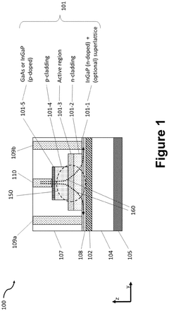
Heterogeneously integrated photonic platform with ingap layers
PatentPendingEP4462618A1
Innovation
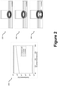
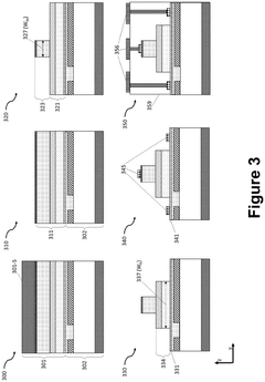
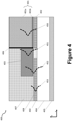
- The development of a heterogeneously integrated laser structure using butt-coupling and mode conversion with a detailed design that includes a high-bandgap InGaP contact layer and a dielectric waveguide structure, allowing for efficient coupling between active and passive waveguides, enabling high-yield bonding and robust semiconductor processing at short wavelengths.
Reliability Testing Standards for Space Photonics
Reliability testing standards for space photonics have evolved significantly to address the unique challenges posed by the harsh environment of space. These standards are critical for ensuring that photonic integrated circuits (PICs) can withstand extreme temperature fluctuations, radiation exposure, vacuum conditions, and mechanical stresses encountered during launch and operation in space.
The International Organization for Standardization (ISO) and the European Space Agency (ESA) have developed comprehensive testing protocols specifically for space photonics. These include the ECSS-Q-ST-60-13C standard, which outlines requirements for radiation hardness assurance, and MIL-STD-883, which provides test methods for microelectronic devices adaptable to photonic components.
Radiation testing forms a cornerstone of these standards, with Total Ionizing Dose (TID) tests simulating accumulated radiation exposure over a mission lifetime. Single Event Effects (SEE) testing evaluates the circuit's resilience against high-energy particle strikes. These tests typically require specialized facilities capable of generating particle beams that mimic space radiation environments.
Thermal cycling tests represent another critical aspect, subjecting PICs to temperature extremes ranging from -170°C to +125°C over hundreds or thousands of cycles. This process reveals potential failure modes related to coefficient of thermal expansion mismatches between different materials in the integrated circuits.
Vacuum testing standards require components to operate in pressures below 10^-6 torr, evaluating outgassing properties and potential for contamination of optical surfaces. The ASTM E595 standard specifically addresses material outgassing characteristics critical for maintaining optical performance in space.
Mechanical reliability standards include random vibration testing (20-2000 Hz frequency range), shock testing (up to 10,000g), and acoustic testing to simulate launch conditions. These tests follow standards such as NASA-STD-7001B and GSFC-STD-7000A, ensuring PICs can survive the violent mechanical stresses of launch.
Long-term reliability prediction methodologies have also been standardized, incorporating accelerated life testing protocols based on the Arrhenius equation and Weibull statistical analysis. These approaches enable manufacturers to estimate the mean time between failures (MTBF) for photonic components in space applications, typically requiring demonstration of 15+ year operational lifetimes.
Recent updates to these standards have begun incorporating specific provisions for integrated photonics, addressing unique failure modes such as waveguide degradation, optical coupling stability, and laser reliability in radiation environments. The emerging JEDEC JEP180 standard specifically addresses reliability test methods for silicon photonics, representing an important step toward standardization in this rapidly evolving field.
International Collaboration in Space Photonics Research
The field of photonic integrated circuits (PICs) for space exploration has witnessed unprecedented growth in international collaboration over the past decade. Space agencies including NASA, ESA, JAXA, and CNSA have established formal frameworks for joint research initiatives, recognizing that the complex challenges of space photonics require diverse expertise and resources beyond any single nation's capabilities. These collaborations have accelerated technology development while distributing costs across multiple stakeholders.
The International Space Photonics Consortium (ISPC), formed in 2018, represents a milestone in global cooperation, bringing together 27 research institutions from 14 countries. This consortium has standardized testing protocols for space-grade photonic components and established shared facilities for radiation hardness testing, significantly reducing redundant efforts and accelerating qualification processes for flight hardware.
University partnerships have emerged as another crucial dimension of international collaboration. The Space Photonics Research Network connects academic institutions across North America, Europe, and Asia, facilitating researcher exchanges and joint laboratory initiatives. These academic collaborations have proven particularly effective in addressing fundamental research challenges in areas such as radiation-resistant materials and novel waveguide architectures.
Industry-led international partnerships have also flourished, with companies like Airbus, Thales Alenia Space, and Lockheed Martin forming strategic alliances with specialized photonics firms across multiple countries. These partnerships have focused on transitioning laboratory innovations into flight-qualified hardware, addressing the critical "valley of death" between research breakthroughs and practical implementation in space systems.
Data sharing represents perhaps the most transformative aspect of international collaboration in space photonics. The Open Space Photonics Database, launched in 2020, provides researchers worldwide with access to performance data from in-orbit photonic systems, creating an unprecedented resource for understanding how these technologies perform in the actual space environment. This open science approach has accelerated learning cycles and prevented repeated failures across different missions.
Challenges remain in harmonizing intellectual property frameworks across different national jurisdictions, with varying approaches to patent protection and technology transfer creating occasional friction in collaborative projects. Nevertheless, the trend toward greater international cooperation continues to strengthen, with new bilateral and multilateral agreements being established annually, reflecting the growing recognition that space photonics advancement requires global scientific cooperation.
Unlock deeper insights with Patsnap Eureka Quick Research — get a full tech report to explore trends and direct your research. Try now!
Generate Your Research Report Instantly with AI Agent
Supercharge your innovation with Patsnap Eureka AI Agent Platform!