The Role of Photonic Integrated Circuits in Virtual Reality Systems
SEP 29, 202510 MIN READ
Generate Your Research Report Instantly with AI Agent
Patsnap Eureka helps you evaluate technical feasibility & market potential.
PIC Technology Evolution and VR Integration Goals
Photonic Integrated Circuits (PICs) represent a revolutionary advancement in optical technology, miniaturizing complex optical systems onto chip-scale platforms. The evolution of PIC technology has followed a trajectory similar to electronic integrated circuits but with unique challenges related to light manipulation at microscale. Initially developed for telecommunications in the 1980s, PICs have expanded into diverse applications including sensing, biomedical diagnostics, and increasingly, virtual reality systems.
The historical progression of PIC technology shows significant milestones: from basic waveguide structures to complex systems integrating lasers, modulators, detectors, and multiplexers on a single chip. Material platforms have diversified from traditional indium phosphide to include silicon photonics, silicon nitride, and polymer-based solutions, each offering distinct advantages for specific applications. This diversification has been crucial for addressing the multifaceted requirements of emerging technologies like VR.
For virtual reality applications, PIC technology aims to overcome fundamental limitations in current systems. Traditional VR displays suffer from bulkiness, limited field of view, vergence-accommodation conflict, and high power consumption. PICs offer potential solutions through miniaturized optical engines that can deliver higher resolution, wider field of view, and reduced form factor while maintaining energy efficiency. The integration of PICs into VR headsets represents a convergence of optical computing, display technology, and advanced manufacturing techniques.
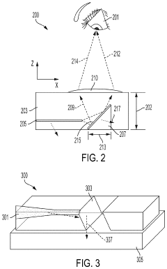
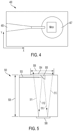
The technical goals for PIC integration in VR systems are multifaceted. Primary objectives include developing waveguide-based display systems that can project images directly onto the retina with unprecedented resolution and field of view. Secondary goals involve creating compact optical tracking systems using PIC-based LiDAR or structured light approaches for precise motion tracking without external sensors. Additionally, researchers aim to implement foveated rendering techniques using PICs to optimize computational resources by focusing rendering detail where the human eye is most sensitive.
Current technological trends indicate a push toward heterogeneous integration, where different material platforms are combined to leverage their respective strengths. Silicon photonics offers high integration density and CMOS compatibility, while III-V materials provide efficient light sources. This hybrid approach is particularly promising for VR applications requiring both high performance and miniaturization.
Looking forward, the roadmap for PIC technology in VR systems includes achieving sub-micron waveguide structures for higher resolution displays, developing efficient on-chip optical phase arrays for beam steering, and integrating advanced sensing capabilities for eye tracking and gesture recognition. These advancements will collectively enable next-generation VR experiences that are more immersive, comfortable, and accessible than current solutions.
The historical progression of PIC technology shows significant milestones: from basic waveguide structures to complex systems integrating lasers, modulators, detectors, and multiplexers on a single chip. Material platforms have diversified from traditional indium phosphide to include silicon photonics, silicon nitride, and polymer-based solutions, each offering distinct advantages for specific applications. This diversification has been crucial for addressing the multifaceted requirements of emerging technologies like VR.
For virtual reality applications, PIC technology aims to overcome fundamental limitations in current systems. Traditional VR displays suffer from bulkiness, limited field of view, vergence-accommodation conflict, and high power consumption. PICs offer potential solutions through miniaturized optical engines that can deliver higher resolution, wider field of view, and reduced form factor while maintaining energy efficiency. The integration of PICs into VR headsets represents a convergence of optical computing, display technology, and advanced manufacturing techniques.
The technical goals for PIC integration in VR systems are multifaceted. Primary objectives include developing waveguide-based display systems that can project images directly onto the retina with unprecedented resolution and field of view. Secondary goals involve creating compact optical tracking systems using PIC-based LiDAR or structured light approaches for precise motion tracking without external sensors. Additionally, researchers aim to implement foveated rendering techniques using PICs to optimize computational resources by focusing rendering detail where the human eye is most sensitive.
Current technological trends indicate a push toward heterogeneous integration, where different material platforms are combined to leverage their respective strengths. Silicon photonics offers high integration density and CMOS compatibility, while III-V materials provide efficient light sources. This hybrid approach is particularly promising for VR applications requiring both high performance and miniaturization.
Looking forward, the roadmap for PIC technology in VR systems includes achieving sub-micron waveguide structures for higher resolution displays, developing efficient on-chip optical phase arrays for beam steering, and integrating advanced sensing capabilities for eye tracking and gesture recognition. These advancements will collectively enable next-generation VR experiences that are more immersive, comfortable, and accessible than current solutions.
Market Analysis for PIC-Enabled VR Applications
The global market for Photonic Integrated Circuits (PICs) in Virtual Reality (VR) applications is experiencing robust growth, driven by increasing demand for more immersive and realistic VR experiences. Current market valuations indicate that the PIC-enabled VR segment reached approximately $1.2 billion in 2022, with projections suggesting a compound annual growth rate of 24% through 2028. This growth trajectory significantly outpaces the broader VR hardware market, which is growing at about 15% annually.
Consumer entertainment represents the largest market segment for PIC-enabled VR applications, accounting for roughly 45% of the total market share. Gaming applications dominate this segment, with users increasingly demanding higher resolution displays, wider field of view, and reduced latency—all areas where PICs offer substantial advantages over traditional electronic solutions.
Professional applications constitute the second-largest market segment at 30%, encompassing fields such as healthcare (surgical training and planning), industrial design, and architectural visualization. These professional applications typically have higher performance requirements and less price sensitivity than consumer applications, making them particularly suitable for early adoption of advanced PIC technologies.
The education and training sector represents approximately 15% of the market, with significant growth potential as educational institutions increasingly incorporate immersive technologies into their curricula. The remaining 10% is distributed across various niche applications including military training, tourism, and real estate visualization.
Geographically, North America leads the market with approximately 40% share, followed by Asia-Pacific at 35% and Europe at 20%. China and South Korea are showing the fastest growth rates within the Asia-Pacific region, driven by substantial government investments in photonics research and manufacturing infrastructure.
Key market drivers include the push for miniaturization of VR headsets, demand for higher resolution displays, requirements for reduced power consumption, and the need for increased data processing capabilities. PICs address these needs by enabling more efficient light manipulation, reduced form factors, and lower power requirements compared to electronic-only solutions.
Market barriers include high initial manufacturing costs, complex integration challenges with existing electronic systems, and limited production capacity for specialized photonic components. However, these barriers are gradually being overcome through increased investment in manufacturing infrastructure and the development of standardized design and fabrication processes.
The competitive landscape features both established photonics companies expanding into VR applications and VR hardware manufacturers developing in-house photonics capabilities. Strategic partnerships between photonics specialists and VR system integrators are becoming increasingly common, indicating a trend toward collaborative innovation in this rapidly evolving market space.
Current PIC Implementation Challenges in VR
Despite significant advancements in photonic integrated circuit (PIC) technology, implementing PICs in virtual reality systems presents several substantial challenges. The miniaturization requirements for VR headsets create severe space constraints for PIC integration. Current PIC designs often require several square centimeters of real estate, which conflicts with the trend toward lighter, more compact VR devices. This dimensional incompatibility necessitates novel approaches to PIC architecture and packaging to achieve the necessary form factors.
Thermal management represents another critical challenge. PICs generate considerable heat during operation, particularly when handling the high data throughput required for immersive VR experiences. In the confined space of a head-mounted display, this heat can lead to performance degradation, reduced component lifespan, and user discomfort. Existing cooling solutions are often bulky or power-intensive, further complicating integration efforts.
Power consumption remains a significant obstacle, especially for wireless VR applications. Current PIC implementations typically require several watts of power, which quickly depletes battery reserves in portable systems. The energy requirements for high-resolution, high-frame-rate displays further exacerbate this issue, creating a fundamental tension between performance and operational longevity.
Manufacturing complexity and associated costs present substantial barriers to widespread adoption. PICs require specialized fabrication processes with extremely tight tolerances, often utilizing exotic materials that are difficult to integrate with conventional CMOS manufacturing. This manufacturing divergence results in higher production costs and lower yields compared to electronic integrated circuits, limiting commercial viability for mass-market VR applications.
Coupling efficiency between optical components represents a persistent technical challenge. The interfaces between PICs and other optical elements in VR systems, such as waveguides and micro-displays, suffer from significant signal losses. These coupling inefficiencies can reach 50% or more, necessitating higher initial power inputs and contributing to the aforementioned thermal and power consumption issues.
Standardization remains underdeveloped in the PIC ecosystem, with multiple competing platforms and protocols. This fragmentation complicates integration efforts and inhibits economies of scale. Unlike the electronic semiconductor industry, which benefits from well-established standards, the photonic integration landscape lacks unified approaches to design, testing, and implementation specifically tailored for VR applications.
Achieving the necessary optical performance for VR applications presents additional challenges. Current PICs struggle to simultaneously deliver the wide field of view, high resolution, and low latency required for truly immersive experiences. The complex optical pathways needed for eye tracking, foveated rendering, and other advanced VR features further complicate PIC design and implementation.
State-of-the-Art PIC Solutions for VR Systems
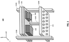
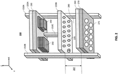
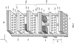
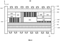
01 Integration of optical components on a single chip
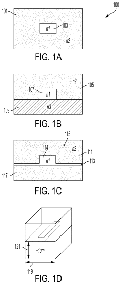
Photonic integrated circuits (PICs) involve the integration of multiple optical components such as waveguides, modulators, detectors, and light sources on a single chip. This integration enables miniaturization of optical systems while maintaining or improving performance. The technology allows for complex optical functionalities to be implemented in a compact form factor, reducing size, weight, and power consumption compared to discrete optical components.- Integration of optical components on photonic integrated circuits: Photonic integrated circuits (PICs) involve the integration of multiple optical components such as waveguides, modulators, detectors, and light sources on a single chip. This integration enables compact, high-performance optical systems with reduced size, weight, and power consumption compared to discrete optical components. The integration techniques include monolithic integration on materials like silicon, indium phosphide, or silicon nitride, allowing for complex optical functionalities in telecommunications, data centers, and sensing applications.
- Silicon photonics technology for high-speed data transmission: Silicon photonics technology enables the fabrication of photonic integrated circuits using CMOS-compatible processes, facilitating the integration of optical and electronic components on the same chip. This technology is particularly valuable for high-speed data transmission applications, offering bandwidth capabilities exceeding electronic interconnects while maintaining energy efficiency. Silicon photonic devices include high-speed modulators, photodetectors, and wavelength division multiplexing components that support data rates of multiple terabits per second for next-generation computing and communication systems.
- Novel waveguide structures and designs for PICs: Advanced waveguide structures are fundamental to photonic integrated circuits, enabling efficient light propagation, manipulation, and coupling. These structures include strip waveguides, rib waveguides, slot waveguides, and photonic crystal waveguides, each offering specific advantages for different applications. Novel waveguide designs focus on minimizing propagation losses, enhancing mode confinement, reducing bend radii, and enabling polarization management. These innovations allow for more compact circuit layouts, improved performance, and expanded functionality in applications ranging from telecommunications to quantum computing.
- Heterogeneous integration of III-V materials with silicon photonics: Heterogeneous integration combines the light-emitting capabilities of III-V semiconductor materials with the processing advantages of silicon photonics. This approach addresses silicon's inherent limitation in light generation by bonding or growing III-V materials (such as indium phosphide or gallium arsenide) onto silicon substrates. The resulting hybrid platforms enable efficient lasers, amplifiers, and photodetectors directly integrated with silicon waveguides. Various bonding techniques, including direct wafer bonding, adhesive bonding, and epitaxial growth methods, are employed to achieve this integration while maintaining optical performance and reliability.
- Packaging and fiber coupling solutions for photonic integrated circuits: Efficient packaging and fiber coupling are critical challenges in photonic integrated circuit deployment. Advanced solutions include edge coupling, grating couplers, and mode size converters to efficiently transfer light between optical fibers and on-chip waveguides. Packaging technologies address thermal management, hermetic sealing, and electrical connections while maintaining optical alignment precision. Automated assembly processes, passive alignment features, and integrated optical interposers help reduce coupling losses and packaging costs. These innovations enable the practical implementation of PICs in real-world applications by bridging the gap between chip-scale photonics and fiber-optic networks.
02 Silicon photonics and material platforms
Various material platforms are used for photonic integrated circuits, with silicon photonics being particularly prominent due to its compatibility with CMOS manufacturing processes. Other materials include III-V semiconductors, silicon nitride, lithium niobate, and polymer-based platforms. Each material system offers different advantages in terms of optical properties, integration capabilities, and application-specific performance. Hybrid integration approaches combine different materials to leverage their respective strengths.Expand Specific Solutions03 Coupling and interconnect technologies
Efficient coupling between photonic integrated circuits and external optical components or fibers is crucial for system performance. Various coupling techniques include edge coupling, grating couplers, and tapered waveguides. On-chip optical interconnects enable communication between different sections of the PIC or between multiple chips. Advanced coupling solutions address challenges related to alignment tolerance, polarization sensitivity, and bandwidth limitations while minimizing insertion losses.Expand Specific Solutions04 Integration with electronic circuits
The co-integration of photonic and electronic circuits creates powerful optoelectronic systems that leverage the advantages of both domains. Electronic-photonic integration approaches include monolithic integration, where both electronic and photonic components are fabricated on the same substrate, and hybrid integration using techniques like flip-chip bonding. These integrated circuits enable high-speed data processing, efficient signal conversion between optical and electrical domains, and advanced sensing capabilities.Expand Specific Solutions05 Applications in telecommunications and data centers
Photonic integrated circuits are widely deployed in telecommunications infrastructure and data centers to meet increasing bandwidth demands. Applications include optical transceivers for high-speed data transmission, wavelength division multiplexing systems, optical switches, and signal processing elements. PICs enable higher data rates, longer transmission distances, and reduced energy consumption compared to traditional electronic solutions, making them essential components in modern communication networks.Expand Specific Solutions
Leading Companies in PIC and VR Ecosystem
The photonic integrated circuits (PICs) market in virtual reality systems is in a growth phase, with increasing market size driven by demand for higher performance VR experiences. The technology is approaching maturity but still evolving, with key players demonstrating varying levels of advancement. Companies like Intel, PsiQuantum, and Magic Leap are leading innovation in photonic integration for VR applications, while display specialists including BOE Technology Group and China Star Optoelectronics are incorporating PICs into their visual systems. Telecommunications giants such as Huawei and academic institutions like UC Berkeley (through nEye Systems) are advancing the underlying optical technologies. Taiwan Semiconductor and other manufacturers are working to scale production capabilities, indicating the technology's transition toward commercial viability in next-generation VR systems.
PsiQuantum Corp.
Technical Solution: PsiQuantum has adapted their quantum photonic technology for VR applications, creating ultra-high-bandwidth PICs that leverage quantum properties for enhanced performance. Their approach utilizes silicon nitride waveguides with proprietary quantum dot integration for efficient light generation and manipulation. PsiQuantum's PICs feature quantum-enhanced photodetectors that achieve near-single-photon sensitivity, enabling extremely low-power operation critical for mobile VR systems. Their technology incorporates specialized entangled photon sources that can be used for secure data transmission within VR environments, addressing growing privacy concerns. PsiQuantum has developed unique optical switching architectures that achieve sub-picosecond switching times, enabling ultra-low latency data transmission essential for immersive VR experiences. Their photonic chips utilize specialized non-linear optical materials integrated directly into the waveguide structures, allowing for efficient wavelength conversion and signal processing. Recent developments include the integration of quantum random number generators directly on their photonic chips to enhance encryption for sensitive VR applications in enterprise and defense sectors.
Strengths: PsiQuantum's quantum-enhanced technology offers theoretical performance advantages over conventional photonics, particularly in terms of power efficiency and security features. Their specialized fabrication techniques result in exceptionally low optical losses. Weaknesses: The technology remains relatively expensive and challenging to manufacture at scale. Their quantum-enhanced features may be overengineered for many consumer VR applications, creating unnecessary cost and complexity.
Intel Corp.
Technical Solution: Intel has developed silicon photonics technology specifically targeting VR applications through their RealSense platform. Their photonic integrated circuits (PICs) combine multiple optical components on a single chip, enabling high-bandwidth data transmission with significantly reduced latency compared to traditional electronic circuits. Intel's PICs utilize wavelength division multiplexing (WDM) to transmit multiple data streams simultaneously through a single optical waveguide, achieving data rates exceeding 400 Gbps. This technology integrates directly with their neuromorphic computing chips to process visual data for VR applications with minimal power consumption. Intel has also pioneered hybrid integration approaches that combine silicon photonics with III-V materials to create efficient on-chip light sources, crucial for compact VR headset designs. Their recent developments include integrated optical phased arrays for beam steering applications in next-generation VR display technologies.
Strengths: Intel's mature silicon fabrication infrastructure allows for cost-effective mass production of PICs. Their vertical integration of computing and photonics technologies creates a comprehensive ecosystem for VR applications. Weaknesses: Their solutions typically require active cooling systems, increasing the overall size and weight of VR headsets. The technology also faces challenges in achieving the ultra-low latency required for fully immersive VR experiences.
Key Patents and Research in PIC-VR Integration
Photonic integrated circuits and low-coherence interferometry for in-field sensing
PatentInactiveUS20240061170A1
Innovation
- The development of a fully integrated photonic integrated circuit system with novel optical input/output couplers and beam shaping optics for out-of-plane in-field sensing, featuring reduced dispersion and high integration, enabling compact and high-see-through quality, suitable for AR/VR headsets and eye tracking systems.
Photonic integrated circuit packages with scalable heterogeneous integration
PatentPendingEP4456134A1
Innovation
- The implementation of a microelectronic assembly with a stack of microelectronic units that enable both vertical and horizontal optical communications, featuring light source layers, an optical interconnect layer, and pillars for power and mechanical support, along with a channel for enhanced heat dissipation, allowing for increased scalability and improved thermo-mechanical capabilities.
Thermal Management Strategies for PIC-VR Systems
The integration of Photonic Integrated Circuits (PICs) in Virtual Reality (VR) systems introduces significant thermal management challenges that must be addressed to ensure optimal performance and reliability. As PICs process high volumes of optical data at unprecedented speeds, they generate substantial heat that can compromise both the optical components and the user experience if not properly managed.
Conventional cooling methods such as passive heat sinks and fans prove inadequate for PIC-VR applications due to the compact form factor requirements and the proximity to the user's face. This necessitates innovative thermal management strategies specifically tailored for these systems.
Microfluidic cooling channels embedded within PIC substrates represent one of the most promising approaches. These microscale channels allow for targeted cooling of hotspots by circulating thermally conductive fluids directly through the substrate material. Recent implementations have demonstrated temperature reductions of up to 35°C compared to passive cooling methods, while adding minimal bulk to the overall system design.
Phase-change materials (PCMs) offer another effective solution by absorbing excess heat during operation through their solid-to-liquid transition. Silicon-based PCMs with melting points between 40-60°C have shown particular promise for PIC-VR applications, providing thermal buffering during peak processing loads while maintaining temperatures below critical thresholds for optical performance degradation.
Advanced thermal interface materials (TIMs) with enhanced thermal conductivity are being developed specifically for PIC applications. Graphene-enhanced TIMs have demonstrated thermal conductivity values exceeding 25 W/mK, significantly outperforming traditional thermal compounds while maintaining the flexibility required for VR headset designs.
Distributed thermal sensors and dynamic thermal management systems represent the cutting edge of PIC-VR thermal solutions. These systems employ arrays of microscale temperature sensors integrated directly into the photonic circuits, providing real-time thermal mapping. This data feeds into algorithms that dynamically adjust optical routing and processing loads to prevent localized hotspots from forming.
The industry is increasingly moving toward heterogeneous integration approaches that strategically position heat-generating components to optimize thermal dissipation pathways. By physically separating high-power laser sources from temperature-sensitive modulators and detectors, these designs can reduce thermal crosstalk while maintaining the compact form factors required for VR applications.
Future thermal management strategies will likely incorporate AI-driven predictive cooling systems that anticipate thermal loads based on application demands and user behavior patterns, activating cooling mechanisms preemptively rather than reactively.
Manufacturing Scalability of PICs for Consumer VR
The manufacturing scalability of Photonic Integrated Circuits (PICs) represents a critical factor in their widespread adoption for consumer Virtual Reality (VR) applications. Current manufacturing processes for PICs face significant challenges when transitioning from laboratory-scale production to mass manufacturing required for consumer electronics markets. The primary fabrication methods include silicon photonics platforms, indium phosphide-based integration, and silicon nitride processes, each with distinct scalability profiles.
Silicon photonics manufacturing has benefited substantially from leveraging existing CMOS infrastructure, allowing for relatively high-volume production compared to other PIC platforms. Major semiconductor foundries have begun offering silicon photonics process design kits (PDKs), enabling fabless companies to design PICs without investing in fabrication facilities. However, the integration of optical components with different material requirements still presents yield challenges at scale.
Indium phosphide-based PICs offer superior light emission capabilities essential for VR applications but face more significant manufacturing scalability hurdles. The specialized equipment and processes required for III-V semiconductor fabrication limit production capacity and increase unit costs. Recent advances in heterogeneous integration, where different materials are bonded together, show promise for combining the manufacturing advantages of silicon with the optical performance of III-V materials.
Yield management represents a particular challenge for PIC manufacturing in the VR context. The complex optical structures required for VR applications demand nanometer-scale precision, where even minor fabrication variations can significantly impact device performance. Statistical process control methods adapted from the semiconductor industry are being implemented to improve yield rates, though they require further refinement for photonic-specific parameters.
Cost structures for PIC manufacturing currently prohibit mass-market VR adoption. While silicon photonics benefits from economies of scale, the specialized packaging requirements for optical interfaces add substantial costs. Industry analysts project that PIC costs need to decrease by approximately 60-70% to meet consumer VR price points. Automated testing procedures are being developed to reduce quality assurance costs, which currently represent up to 30% of production expenses.
Supply chain development for PIC manufacturing remains in its early stages compared to mature electronic component ecosystems. The specialized materials, equipment, and expertise required create potential bottlenecks as production volumes increase. Strategic partnerships between foundries, design houses, and packaging specialists are forming to address these limitations, though significant investment in manufacturing infrastructure is still needed to support consumer VR-scale production volumes.
Unlock deeper insights with Patsnap Eureka Quick Research — get a full tech report to explore trends and direct your research. Try now!
Generate Your Research Report Instantly with AI Agent
Supercharge your innovation with Patsnap Eureka AI Agent Platform!