Research on Photonic Integrated Circuits Within Industrial Automation
SEP 29, 202510 MIN READ
Generate Your Research Report Instantly with AI Agent
Patsnap Eureka helps you evaluate technical feasibility & market potential.
PIC Technology Background and Objectives
Photonic Integrated Circuits (PICs) represent a revolutionary technology that integrates multiple photonic functions on a single chip, similar to electronic integrated circuits but utilizing light instead of electrons. The evolution of PICs began in the 1980s with rudimentary optical waveguides and has since progressed through several technological generations, each marked by increasing integration density and functionality.
The development trajectory of PIC technology has been characterized by continuous miniaturization, improved performance, and expanded application domains. Initially focused on telecommunications, PICs have gradually expanded into sensing, biomedical applications, and more recently, industrial automation. This technological progression has been driven by advancements in materials science, fabrication techniques, and design methodologies.
Current trends in PIC technology include the integration of heterogeneous materials, the development of programmable photonic circuits, and the convergence with electronic integrated circuits to form electro-photonic integrated systems. These trends are reshaping the capabilities and potential applications of PICs across various industries, particularly in industrial automation where high-speed, electromagnetic interference-resistant communication is crucial.
The primary objective of researching PICs within industrial automation is to leverage the inherent advantages of photonic technology—such as high bandwidth, low latency, and immunity to electromagnetic interference—to address the growing demands of Industry 4.0 and smart manufacturing. Specifically, PICs aim to enable real-time data processing, ultra-fast communication between industrial systems, and precise sensing capabilities in harsh industrial environments.
Another key goal is to overcome the limitations of traditional electronic systems in industrial settings, including bandwidth constraints, susceptibility to electromagnetic interference, and heat generation. PICs offer a promising alternative that can potentially revolutionize industrial control systems, sensor networks, and communication infrastructure.
Furthermore, the research aims to develop cost-effective, energy-efficient PIC solutions that can be mass-produced and easily integrated into existing industrial frameworks. This includes exploring novel fabrication techniques, standardizing interfaces, and creating modular PIC designs that can be customized for specific industrial applications.
Long-term objectives include establishing a comprehensive ecosystem for PIC-based industrial automation, encompassing design tools, manufacturing processes, testing methodologies, and application-specific integrated solutions. This ecosystem would facilitate the widespread adoption of PIC technology in industrial settings, driving efficiency improvements, enabling new capabilities, and fostering innovation across the manufacturing sector.
Market Demand Analysis for Industrial Automation PICs
The industrial automation sector is witnessing a significant transformation driven by the integration of advanced technologies, with Photonic Integrated Circuits (PICs) emerging as a critical enabler for next-generation automation systems. Market analysis indicates robust growth potential for PICs in industrial automation, with the global market projected to reach $3.5 billion by 2027, growing at a CAGR of approximately 25% from 2022.
This growth is primarily fueled by increasing demands for higher data processing speeds, reduced latency, and enhanced reliability in industrial control systems. Traditional electronic circuits are approaching their physical limitations in terms of speed and power consumption, creating a substantial market gap that PICs are uniquely positioned to fill. Industries such as manufacturing, energy, and logistics are actively seeking solutions that can handle the massive data throughput required for real-time monitoring and control of complex industrial processes.
The demand for PICs in industrial automation is particularly strong in applications requiring immunity to electromagnetic interference (EMI), which is common in factory environments. Survey data from industrial automation system integrators reveals that over 70% of manufacturing facilities experience operational disruptions due to EMI-related issues, highlighting a significant market need that photonic solutions can address.
Energy efficiency represents another critical market driver, with industrial facilities under increasing pressure to reduce power consumption. PICs offer up to 80% reduction in energy usage compared to traditional electronic circuits for equivalent data processing tasks, making them attractive for energy-intensive industrial operations seeking to minimize operational costs and carbon footprint.
The market for sensing applications within industrial automation shows exceptional promise for PIC technology. Distributed fiber optic sensing systems for structural health monitoring, temperature sensing, and vibration detection are experiencing demand growth exceeding 30% annually. This trend is particularly evident in high-value infrastructure monitoring and precision manufacturing, where conventional sensing technologies cannot deliver the required performance.
Regional analysis indicates that while North America and Europe currently lead in PIC adoption for industrial applications, the Asia-Pacific region is expected to demonstrate the highest growth rate over the next five years. This is attributed to rapid industrialization, substantial manufacturing capacity expansion, and government initiatives promoting smart manufacturing technologies in countries like China, Japan, and South Korea.
Customer surveys indicate that while cost remains a barrier to widespread adoption, with current PIC solutions commanding a premium of 30-50% over conventional alternatives, 65% of industrial automation system architects express willingness to invest in photonic technology given its performance advantages and long-term operational benefits.
Current State and Challenges in Photonic Integration
Photonic Integrated Circuits (PICs) have emerged as a transformative technology in industrial automation, offering significant advantages over traditional electronic circuits in terms of speed, bandwidth, and energy efficiency. Currently, the global market for PICs is experiencing robust growth, with a compound annual growth rate exceeding 25% and projected to reach $3.5 billion by 2025, driven largely by industrial applications.
The state of photonic integration technology has advanced considerably in recent years, with several key platforms dominating the landscape. Silicon photonics has emerged as the leading platform due to its compatibility with CMOS fabrication processes, enabling high-volume, low-cost production. Alternative platforms include Indium Phosphide (InP), which excels in active components like lasers and amplifiers, and Silicon Nitride (SiN), which offers superior performance for passive components and low-loss waveguides.
Despite these advancements, significant technical challenges persist in the widespread adoption of PICs in industrial automation. Integration density remains a critical limitation, with current commercial PICs typically accommodating hundreds of components per chip, far below the millions achieved in electronic integrated circuits. This integration bottleneck restricts the complexity and functionality of photonic systems in industrial settings.
Coupling efficiency between different photonic components and between photonic and electronic systems represents another major challenge. Current coupling losses often exceed 1 dB per interface, significantly degrading overall system performance in complex industrial automation applications that require multiple interconnections.
Temperature sensitivity poses a substantial obstacle for industrial environments, where operating conditions can vary widely. Most photonic components exhibit significant wavelength drift with temperature fluctuations (typically 70-80 pm/°C for silicon waveguides), necessitating precise temperature control systems that add complexity and cost to industrial implementations.
Manufacturing yield and reliability issues further complicate industrial adoption. Current fabrication processes for PICs achieve yields of 60-80% for complex designs, compared to >95% for mature electronic ICs. This disparity increases production costs and limits scalability for industrial applications requiring high reliability.
Geographically, photonic integration research and development is concentrated in specific regions. North America leads in silicon photonics research, with major industrial players and research institutions primarily located in the United States. Europe maintains strength in InP-based integration, particularly in countries like the Netherlands and Germany. The Asia-Pacific region, especially China, Japan, and Singapore, is rapidly expanding its capabilities across multiple integration platforms.
Standardization remains underdeveloped compared to electronic circuits, with limited industry-wide agreement on design rules, component libraries, and testing methodologies. This lack of standardization impedes interoperability and increases development costs for industrial automation applications.
Current PIC Solutions for Industrial Automation
01 Integration of optical components on a single chip
Photonic integrated circuits (PICs) involve the integration of multiple optical components such as waveguides, modulators, detectors, and light sources on a single chip. This integration enables compact, high-performance optical systems with reduced size, weight, and power consumption compared to discrete optical components. The integration technology allows for complex optical functionalities while maintaining signal integrity and minimizing optical losses at component interfaces.- Integration of optical components on a single chip: Photonic integrated circuits (PICs) involve the integration of multiple optical components such as waveguides, modulators, detectors, and light sources on a single chip. This integration enables miniaturization of optical systems while maintaining or improving performance. The technology allows for complex optical functionalities to be implemented in a compact form factor, reducing size, weight, and power consumption compared to discrete optical components.
- Silicon photonics for high-speed data transmission: Silicon photonics technology enables the fabrication of photonic integrated circuits using standard CMOS manufacturing processes. These circuits can achieve high-speed data transmission for telecommunications and data center applications. By leveraging silicon as a platform material, manufacturers can produce cost-effective, energy-efficient optical interconnects that overcome bandwidth limitations of traditional electronic circuits while benefiting from existing semiconductor fabrication infrastructure.
- Heterogeneous integration of materials for enhanced functionality: Heterogeneous integration combines different material platforms such as silicon, III-V semiconductors, and lithium niobate to create photonic integrated circuits with enhanced functionality. This approach allows the integration of active components (lasers, amplifiers) with passive waveguides and other optical elements. By leveraging the optimal properties of each material, these hybrid PICs can achieve superior performance in applications requiring both light generation and manipulation.
- Packaging and coupling techniques for PICs: Advanced packaging and coupling techniques are essential for connecting photonic integrated circuits to external optical fibers and electronic components. These methods include edge coupling, grating couplers, and 3D integration approaches that minimize insertion losses while maintaining alignment stability. Effective packaging solutions address thermal management, mechanical protection, and electrical connections, enabling PICs to function reliably in real-world applications while facilitating volume manufacturing.
- Novel waveguide structures and design methodologies: Innovative waveguide structures and design methodologies enhance the performance of photonic integrated circuits. These include subwavelength gratings, photonic crystals, and metamaterial-based waveguides that provide precise control over light propagation. Advanced design tools incorporating electromagnetic simulations and optimization algorithms enable the development of complex optical circuits with improved functionality. These novel approaches address challenges in mode conversion, polarization handling, and wavelength management within compact PIC footprints.
02 Silicon photonics and material platforms
Various material platforms are used for photonic integrated circuits, with silicon photonics being particularly prominent due to its compatibility with CMOS manufacturing processes. Other materials include III-V semiconductors, silicon nitride, lithium niobate, and polymer-based platforms. Each material system offers specific advantages for different applications, such as low propagation loss, high electro-optic coefficients, or efficient light emission. Hybrid integration approaches combine different materials to leverage their complementary properties.Expand Specific Solutions03 Optical interconnects and data communications
Photonic integrated circuits are increasingly used for optical interconnects in data centers and high-performance computing systems. These PICs enable high-bandwidth, energy-efficient data transmission through wavelength division multiplexing, advanced modulation formats, and integrated transceivers. The technology addresses bandwidth bottlenecks in traditional electronic interconnects while reducing power consumption for data movement, supporting higher data rates and longer transmission distances.Expand Specific Solutions04 Quantum photonics and specialized applications
Photonic integrated circuits are enabling emerging applications in quantum computing, sensing, and communications. These specialized PICs incorporate components for generating, manipulating, and detecting quantum states of light, such as single-photon sources, entangled photon pair generators, and quantum gates. Other specialized applications include integrated optical gyroscopes, LiDAR systems for autonomous vehicles, biomedical sensing platforms, and microwave photonics for signal processing in telecommunications.Expand Specific Solutions05 Packaging and integration with electronics
Advanced packaging technologies are critical for photonic integrated circuits to interface with electronic systems and the outside world. These include fiber-to-chip coupling methods, electronic-photonic co-packaging, and 3D integration approaches. Challenges in thermal management, optical alignment, and hermetic sealing are addressed through innovative packaging solutions. The co-integration of photonics with electronics enables complete systems-on-chip that combine the processing power of electronics with the communication bandwidth of photonics.Expand Specific Solutions
Key Industry Players in Photonic Integration
Photonic Integrated Circuits (PICs) in industrial automation are transitioning from early development to commercial adoption, with the market expected to grow significantly due to increasing demand for high-speed data processing and energy efficiency. The technology maturity varies across players, with established semiconductor giants like TSMC, Intel, and IBM leveraging their manufacturing expertise to develop advanced PIC solutions. Research institutions such as MIT and University of California are driving fundamental innovations, while specialized companies like Lightmatter and Wave Photonics focus on application-specific implementations. Emerging players like Advanced Micro Foundry are establishing specialized foundry services, indicating the ecosystem's evolution toward manufacturing scalability. The competitive landscape reflects a blend of established semiconductor companies expanding their portfolios and specialized photonics startups addressing niche industrial automation applications.
International Business Machines Corp.
Technical Solution: IBM has pioneered silicon nanophotonics technology for industrial automation applications, focusing on ultra-dense integration of optical and electrical components. Their platform incorporates optical transceivers directly onto CMOS chips, achieving data rates of 25 Gbps per channel with multiplexing capabilities that enable aggregate bandwidths exceeding 1 Tbps. IBM's approach utilizes wavelength division multiplexing (WDM) with up to 64 channels on a single waveguide. For industrial automation, IBM has developed specialized photonic integrated circuits that maintain signal integrity across factory floors spanning hundreds of meters while consuming only 5pJ/bit of energy. Their technology incorporates radiation-hardened designs suitable for harsh industrial environments where electromagnetic interference is prevalent. IBM has also implemented on-chip optical sensing capabilities that enable real-time monitoring of manufacturing processes with nanometer-scale precision, facilitating advanced quality control in production lines.
Strengths: IBM offers exceptional integration density and has demonstrated working systems in actual industrial environments with proven reliability. Weaknesses: Their solutions typically require specialized cooling systems and face challenges with cost-effective packaging for mass deployment in industrial settings.
Intel Corp.
Technical Solution: Intel has developed Silicon Photonics technology specifically targeting industrial automation applications. Their integrated photonic circuits combine silicon processing with optical components on a single chip, enabling high-speed data transmission at rates exceeding 100 Gbps. Intel's approach focuses on integrating lasers, modulators, multiplexers, and photodetectors on silicon substrates using their 300mm wafer manufacturing infrastructure. For industrial automation, Intel has created ruggedized photonic transceivers that operate reliably in harsh factory environments with temperature ranges from -40°C to 85°C. Their technology enables deterministic low-latency communication (<1μs) critical for real-time control systems in smart factories. Intel's co-packaged optics solutions reduce power consumption by approximately 30% compared to traditional electrical interconnects, addressing energy efficiency concerns in large-scale industrial deployments.
Strengths: Intel leverages existing CMOS manufacturing infrastructure for cost-effective scaling and has established partnerships with industrial automation leaders for system integration. Weaknesses: Their solutions still face challenges with thermal management in industrial environments and require specialized packaging techniques that increase overall system costs.
Core PIC Patents and Technical Literature Analysis
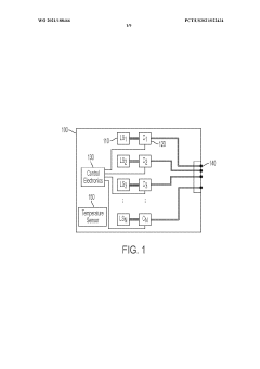
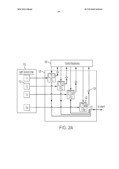
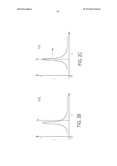
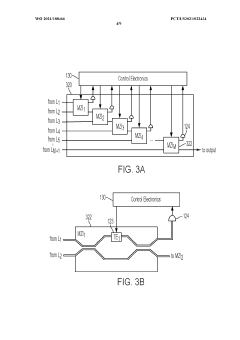
Realizing high per-mode optical power with integrated light sources and optical combiners
PatentWO2021188466A1
Innovation
- An optical chip and package design incorporating a light source array and an optical combiner, where the combiner combines multiple optical signals from light sources such as diode lasers or VCSELs to produce a high-power, single-mode optical signal, utilizing tunable elements like phase shifters and control electronics to enhance output power.
Integrated photonic-electronic circuits and systems
PatentInactiveUS7251386B1
Innovation
- Integrated photonic-electronic circuit chips using group IV materials, which combine electronic and photonic portions to enable optical signal transmission and reception, allowing for reconfigurability and flexible communication through both optical and electrical means, and supporting high-speed data transfer rates.
Manufacturing Processes and Scalability Considerations
The manufacturing processes for photonic integrated circuits (PICs) present unique challenges compared to traditional electronic integrated circuits. Current PIC fabrication primarily relies on semiconductor manufacturing techniques adapted for optical components, with silicon photonics emerging as the dominant platform due to its compatibility with CMOS processes. The manufacturing workflow typically involves wafer preparation, lithography, etching, deposition, and packaging stages, each requiring precise control to achieve the nanometer-scale features necessary for optical functionality.
A critical manufacturing challenge for industrial automation applications is maintaining tight dimensional tolerances. Even minor deviations in waveguide dimensions can significantly alter optical properties, affecting signal integrity in automation systems. This necessitates advanced process control strategies and in-line metrology techniques specifically developed for photonic structures. Manufacturers are increasingly implementing automated optical inspection systems and machine learning algorithms to detect fabrication anomalies before they impact device performance.
Material selection represents another key consideration in PIC manufacturing scalability. While silicon-on-insulator (SOI) platforms offer manufacturing maturity, they face limitations in certain optical functionalities. Alternative material systems such as silicon nitride, indium phosphide, and lithium niobate provide enhanced performance characteristics but present integration challenges with existing semiconductor infrastructure. Hybrid integration approaches combining multiple material platforms are gaining traction to leverage the strengths of each material system.
Packaging and assembly processes constitute a substantial portion of PIC production costs, often exceeding 80% of total manufacturing expenses. The requirement for precise fiber-to-chip coupling, thermal management, and electrical connections presents significant scaling barriers. Recent innovations in automated assembly techniques, including machine vision-guided placement and passive alignment structures, are gradually reducing these bottlenecks. Standardization efforts across the industry are also emerging to establish common interfaces and packaging formats.
Scalability considerations extend beyond technical aspects to economic factors. Current PIC production volumes remain relatively low compared to electronic ICs, resulting in higher per-unit costs. The transition to high-volume manufacturing requires significant capital investment in specialized equipment and process development. Industry consortia and foundry services are emerging to distribute these costs across multiple users, enabling smaller companies to access advanced fabrication capabilities without prohibitive investment. This shared infrastructure model is particularly beneficial for industrial automation applications, where customized solutions may be required for specific sensing or control functions.
Standards and Interoperability in Industrial PIC Systems
The standardization landscape for Photonic Integrated Circuits (PICs) in industrial automation remains fragmented, with multiple organizations working to establish unified frameworks. Key standards bodies including the International Electrotechnical Commission (IEC), Institute of Electrical and Electronics Engineers (IEEE), and Optical Internetworking Forum (OIF) have begun developing specifications specifically addressing industrial PIC implementations. These efforts focus on ensuring consistent performance metrics, reliability parameters, and interoperability protocols across different manufacturers' components.
Interoperability challenges present significant barriers to widespread PIC adoption in industrial settings. Current industrial automation systems utilize diverse communication protocols such as PROFINET, EtherCAT, and OPC UA, necessitating standardized interfaces between photonic components and existing industrial networks. The development of middleware solutions and protocol translation layers has emerged as a critical focus area, with several industry consortia proposing reference architectures for seamless integration.
Physical interface standardization represents another crucial dimension, encompassing optical connectors, waveguide coupling specifications, and fiber attachment methodologies. The industry has seen progress with initiatives like the PIC Manufacturing Automation Project (PIC-MAP) establishing common mechanical interfaces and tolerances for automated assembly processes. These standards enable interchangeability of components from different suppliers, fostering a more competitive and innovative ecosystem.
Data format compatibility across the optical-electrical boundary requires particular attention in industrial environments. Standards defining signal encoding, modulation schemes, and error correction protocols specific to industrial PIC applications are being developed by joint working groups comprising both photonics and industrial automation experts. These efforts aim to ensure deterministic performance and real-time capabilities essential for mission-critical industrial control systems.
Testing and certification frameworks represent the final pillar of the standardization landscape. Organizations including the Photonic Integration Technology Center (PITC) have proposed comprehensive validation methodologies covering optical performance, environmental resilience, and long-term reliability. These frameworks incorporate accelerated aging protocols and stress testing specifically calibrated for industrial operating conditions, ensuring PICs can withstand harsh factory environments.
The convergence of these standardization efforts will ultimately determine the pace of PIC adoption in industrial automation. Companies actively participating in standards development gain strategic advantages through early alignment with emerging specifications, while also influencing technical requirements to match their capabilities. As these standards mature over the next 3-5 years, they will likely catalyze significant market expansion by reducing integration costs and technical risks.
Unlock deeper insights with Patsnap Eureka Quick Research — get a full tech report to explore trends and direct your research. Try now!
Generate Your Research Report Instantly with AI Agent
Supercharge your innovation with Patsnap Eureka AI Agent Platform!