How Do Photonic Integrated Circuits Affect Optical Networks
SEP 29, 20259 MIN READ
Generate Your Research Report Instantly with AI Agent
PatSnap Eureka helps you evaluate technical feasibility & market potential.
PIC Technology Background and Objectives
Photonic Integrated Circuits (PICs) represent a revolutionary advancement in optical communication technology, evolving from the fundamental concept of integrating multiple photonic functions onto a single chip. This technology has roots dating back to the 1980s, but has seen accelerated development over the past two decades as demand for higher bandwidth and more efficient optical networks has intensified. The evolution of PICs has been driven by the increasing limitations of electronic integrated circuits in meeting the exponential growth in data traffic and the need for energy-efficient solutions in telecommunications infrastructure.
The technological trajectory of PICs has been characterized by continuous miniaturization, increased functionality, and improved manufacturing processes. Early iterations focused primarily on basic waveguide structures, while contemporary PICs incorporate complex elements including lasers, modulators, detectors, multiplexers, and optical amplifiers on a single substrate. This integration has progressively reduced the size, cost, and power consumption of optical communication systems while simultaneously enhancing their performance capabilities.
The primary objective of PIC technology in optical networks is to overcome the bottlenecks associated with traditional discrete optical components. By integrating multiple optical functions onto a single chip, PICs aim to dramatically reduce the physical footprint of optical networking equipment, decrease power consumption, enhance reliability through reduced component count, and lower overall system costs through economies of scale in manufacturing.
A critical goal for PIC development is achieving seamless integration with existing optical network infrastructure while providing a clear pathway for future network evolution. This includes compatibility with established optical communication protocols and standards, while simultaneously enabling new capabilities such as higher data rates, more efficient wavelength division multiplexing, and advanced modulation formats.
The technology also aims to address the growing bandwidth demands of emerging applications including 5G networks, data center interconnects, high-performance computing, and the anticipated requirements of 6G communications. As these applications continue to drive exponential growth in data traffic, PICs are positioned as a key enabling technology for next-generation optical networks that can deliver terabit-per-second transmission rates with minimal latency and energy consumption.
Looking forward, PIC technology development is increasingly focused on heterogeneous integration approaches that combine different material platforms to leverage their respective advantages. The ultimate objective is to create fully integrated photonic-electronic systems that seamlessly merge the processing capabilities of electronics with the transmission advantages of photonics, potentially revolutionizing not only telecommunications but also sensing, computing, and numerous other applications that rely on optical technologies.
Optical Network Market Demand Analysis
The global optical network market is experiencing unprecedented growth driven by the exponential increase in data traffic and bandwidth demands. According to recent market research, the optical networking market is projected to reach $50 billion by 2028, growing at a CAGR of approximately 7% from 2023. This growth is primarily fueled by the rapid expansion of cloud services, 5G deployments, and the increasing adoption of IoT devices across various industries.
Photonic Integrated Circuits (PICs) are emerging as a critical technology in addressing these escalating bandwidth requirements. Traditional optical networks face significant challenges in meeting the demands for higher data rates, lower latency, and improved energy efficiency. The market is increasingly seeking solutions that can provide terabit-per-second transmission capabilities while maintaining cost-effectiveness and reliability.
Telecommunications operators represent the largest segment of demand, accounting for nearly 40% of the optical networking market. These operators are actively investing in upgrading their infrastructure to support next-generation services and applications. Data center operators follow closely, contributing approximately 30% to the market demand, as they seek to enhance interconnectivity and reduce power consumption in their facilities.
Regionally, North America and Asia-Pacific dominate the optical network market, collectively representing over 65% of global demand. The Asia-Pacific region, particularly China, Japan, and South Korea, is witnessing the fastest growth rate due to aggressive investments in 5G infrastructure and digital transformation initiatives. Europe follows with significant investments in research and development of advanced optical technologies.
The demand for coherent optical solutions incorporating PICs is particularly strong, with market research indicating a growth rate exceeding 15% annually. This surge is attributed to the superior performance characteristics of PIC-based systems, including higher integration density, reduced power consumption, and enhanced reliability compared to discrete optical components.
Enterprise customers across financial services, healthcare, and manufacturing sectors are increasingly adopting optical networks to support their digital transformation initiatives. These sectors require high-speed, secure, and reliable connectivity solutions that can handle massive data transfers and real-time applications.
The market is also witnessing a shift towards open and disaggregated optical networks, with operators seeking flexible and vendor-neutral solutions. This trend is creating new opportunities for PIC technology providers to develop standardized and interoperable components that can be integrated into various network architectures.
Looking forward, the demand for PIC-enabled optical networks is expected to accelerate as emerging applications such as autonomous vehicles, smart cities, and extended reality (XR) gain traction. These applications will require ultra-high bandwidth, minimal latency, and robust connectivity, further driving the adoption of advanced optical networking technologies.
PIC Development Status and Technical Challenges
Photonic Integrated Circuits (PICs) have emerged as a transformative technology in optical networks, yet their development faces significant technical challenges. Currently, PICs are transitioning from research laboratories to commercial applications, with varying maturity levels across different integration platforms. Silicon photonics has achieved the highest integration density and compatibility with CMOS fabrication processes, while Indium Phosphide (InP) platforms excel in active component integration including lasers and amplifiers.
The global landscape of PIC development shows concentration in North America, Europe, and East Asia. The United States leads in silicon photonics research through institutions like MIT, Caltech, and companies such as Intel and Cisco. Europe maintains strength in InP-based integration through research centers in the Netherlands and Germany. Meanwhile, China, Japan, and Singapore are rapidly expanding their PIC manufacturing capabilities and research programs.
Despite significant progress, several technical challenges impede widespread PIC adoption in optical networks. Integration density remains limited compared to electronic integrated circuits, with current commercial PICs typically integrating tens to hundreds of components rather than billions seen in electronic counterparts. This limitation stems from the fundamental size constraints of optical waveguides and the difficulty in miniaturizing certain optical functions.
Coupling efficiency between PICs and optical fibers represents another major challenge. The mode size mismatch between integrated waveguides (typically sub-micron) and standard optical fibers (approximately 10 microns) creates significant coupling losses, often exceeding 3dB per facet. Various coupling structures including grating couplers, spot-size converters, and edge couplers have been developed, but each presents trade-offs between bandwidth, polarization sensitivity, and fabrication complexity.
Thermal management poses additional difficulties as PICs are highly temperature-sensitive. Refractive index variations with temperature can shift resonant wavelengths in filters and modulators, requiring precise temperature control systems or athermal designs. This challenge becomes more pronounced as integration density increases and heat dissipation becomes more concentrated.
Manufacturing yield and reliability present persistent obstacles, particularly for complex PICs. Process variations in fabrication can significantly impact device performance, especially for wavelength-selective components that require nanometer-scale precision. Testing methodologies for PICs remain less mature than those for electronic ICs, complicating quality control processes.
Standardization efforts are still evolving, with multiple competing platforms and packaging approaches limiting interoperability. The lack of unified design tools, process design kits (PDKs), and manufacturing standards increases development costs and time-to-market for PIC-based optical network solutions.
Current PIC Implementation Solutions
01 Integration of optical components on a single chip
Photonic integrated circuits (PICs) involve the integration of multiple optical components such as waveguides, modulators, detectors, and light sources on a single chip. This integration enables miniaturization of optical systems while improving performance, reducing power consumption, and enhancing reliability. The technology allows for complex optical functionalities to be performed within a compact footprint, making it suitable for various applications including telecommunications and data centers.- Integration of optical components on a single chip: Photonic integrated circuits (PICs) involve the integration of multiple optical components such as waveguides, modulators, detectors, and light sources on a single chip. This integration enables compact, high-performance optical systems with reduced size, weight, and power consumption compared to discrete optical components. The integration technology allows for complex optical functionalities while maintaining signal integrity across the chip.
- Silicon photonics manufacturing techniques: Silicon photonics leverages established semiconductor manufacturing processes to create photonic integrated circuits. These techniques include lithography, etching, deposition, and wafer bonding to fabricate optical structures on silicon substrates. The compatibility with CMOS fabrication enables cost-effective mass production of PICs and facilitates the integration of electronic and photonic components on the same chip, leading to enhanced functionality and performance.
- Novel waveguide structures and materials: Advanced waveguide structures and materials are essential for improving the performance of photonic integrated circuits. These include silicon nitride waveguides, polymer waveguides, and hybrid material platforms that offer advantages such as lower propagation losses, wider operational bandwidth, and enhanced nonlinear optical effects. Novel geometries such as slot waveguides, subwavelength gratings, and photonic crystals enable precise control of light propagation and interaction within the PIC.
- Optical interconnects for data communications: Photonic integrated circuits provide high-bandwidth, energy-efficient optical interconnects for data communications in computing systems and telecommunications networks. These optical interconnects overcome the limitations of traditional electrical interconnects by offering higher data rates, lower latency, and reduced power consumption. PICs enable wavelength division multiplexing, allowing multiple data channels to be transmitted simultaneously through a single waveguide, significantly increasing the overall bandwidth capacity.
- Integration with quantum photonic technologies: Photonic integrated circuits are increasingly being used as platforms for quantum photonic technologies. These circuits can generate, manipulate, and detect quantum states of light, enabling applications in quantum computing, quantum communications, and quantum sensing. The integration of single-photon sources, quantum gates, and detectors on a single chip provides a scalable approach to implementing complex quantum photonic systems with improved stability and reduced footprint.
02 Silicon photonics technology
Silicon photonics is a key technology platform for photonic integrated circuits that leverages existing CMOS manufacturing infrastructure. This approach uses silicon as the optical medium for creating waveguides and other photonic components, enabling cost-effective mass production of PICs. Silicon photonics facilitates the integration of optical and electronic components on the same substrate, allowing for high-bandwidth data transmission with reduced energy consumption compared to traditional electronic circuits.Expand Specific Solutions03 Novel waveguide structures and designs
Advanced waveguide structures are fundamental to photonic integrated circuits, enabling efficient light propagation and manipulation. These include strip waveguides, rib waveguides, slot waveguides, and photonic crystal waveguides, each offering specific advantages for different applications. Novel waveguide designs focus on minimizing optical losses, controlling dispersion, enhancing light confinement, and enabling precise routing of optical signals across the photonic chip.Expand Specific Solutions04 Integration of active and passive optical components
Modern photonic integrated circuits combine both active components (lasers, modulators, photodetectors) and passive components (waveguides, splitters, filters) on a single platform. This heterogeneous integration approach overcomes material limitations by incorporating different materials optimized for specific functions. Techniques such as wafer bonding, epitaxial growth, and transfer printing enable the integration of III-V semiconductors with silicon platforms to create fully functional photonic systems with enhanced performance.Expand Specific Solutions05 Packaging and coupling techniques for PICs
Efficient packaging and optical coupling are critical challenges in photonic integrated circuit technology. Various approaches address the interface between PICs and external optical fibers or electronic components, including edge coupling, grating couplers, and 3D integration techniques. Advanced packaging solutions focus on thermal management, hermetic sealing, and alignment precision to maintain optical performance while enabling practical deployment in real-world applications such as telecommunications equipment and sensing systems.Expand Specific Solutions
Key PIC and Optical Network Industry Players
Photonic Integrated Circuits (PICs) are revolutionizing optical networks as the industry transitions from early adoption to commercial scaling. The market is experiencing robust growth, projected to reach $3-5 billion by 2025, driven by increasing bandwidth demands and data center expansion. Technologically, PICs are maturing rapidly with companies at different development stages. Industry leaders like Infinera and Huawei have commercialized PIC-based systems for telecommunications, while Intel, SMART Photonics, and Rockley Photonics are advancing manufacturing processes. Research institutions (MIT, IMEC) are pushing boundaries in integration density and functionality. Emerging players like PsiQuantum and Shanghai Xizhi are exploring novel applications in quantum computing and AI, indicating the technology's expanding potential beyond traditional optical networking.
Infinera Corp.
Technical Solution: Infinera has pioneered photonic integrated circuits (PICs) for optical networks with their proprietary Infinite Capacity Engine (ICE) technology. Their PICs integrate hundreds of optical components onto a single indium phosphide chip, including lasers, modulators, waveguides, and photodetectors. Infinera's latest ICE6 platform delivers 800G per wavelength transmission, enabling network operators to achieve unprecedented capacity and reach. Their vertically integrated approach combines PICs with advanced digital signal processing (DSP) to optimize performance across metro, long-haul, and subsea networks. Infinera's PICs enable super-channels that can be deployed as a single operational entity, dramatically simplifying network management while reducing power consumption and physical footprint by up to 60% compared to discrete component approaches.
Strengths: Industry-leading integration density with hundreds of components on a single chip; proprietary indium phosphide platform enabling monolithic integration of active and passive components; significant power and space savings. Weaknesses: Reliance on proprietary technology may limit ecosystem development; higher initial investment compared to discrete solutions; potential challenges in scaling manufacturing.
Huawei Technologies Co., Ltd.
Technical Solution: Huawei has developed an extensive portfolio of silicon photonics-based PICs for optical networks, focusing on high-speed data center interconnects and telecommunications infrastructure. Their OptiXtrans series leverages PICs to deliver 200G/400G/800G transmission capabilities with significantly reduced power consumption. Huawei's approach combines silicon photonics with advanced packaging techniques to create highly integrated optical-electronic systems. Their silicon photonic chips integrate multiple functions including modulation, multiplexing, and detection on a single die, enabling compact form factors for next-generation optical network equipment. Huawei has also pioneered heterogeneous integration techniques that combine III-V materials with silicon photonics to create complete optical systems-on-chip, addressing the full optical communication chain from light generation to detection.
Strengths: Vertical integration from chip design to network equipment gives end-to-end optimization capabilities; strong R&D investment in advanced packaging and heterogeneous integration; comprehensive product portfolio spanning access to core networks. Weaknesses: Geopolitical challenges affecting global market access; dependency on external foundries for some manufacturing processes; potential interoperability issues with proprietary solutions.
Core PIC Technologies and Patents
Photonic device, system and method of making same
PatentActiveUS20230400627A1
Innovation
- The development of a photonic device with vertically stacked waveguide layers allows for optical power exchange between different photonic layers, enabling the creation of a 3D photonic neural network with reduced chip size, lower fabrication costs, and enhanced computation density.
Photonic integrated circuit with improved signal quality and electrostatic discharge threshold
PatentActiveUS20100247028A1
Innovation
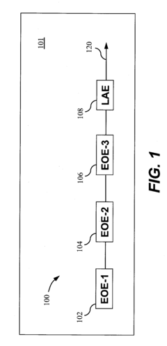
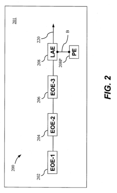
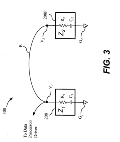
- Incorporating a light-absorbing electro-optic element and a parallel electro-optic element, such as a capacitor, within the signal channel to reduce optical signal power loss, minimize RF crosstalk, and enhance electrostatic discharge resistance, while maintaining desired optical characteristics and performance monitoring capabilities.
Energy Efficiency and Sustainability Impact
Photonic Integrated Circuits (PICs) represent a significant advancement in optical network technology, offering substantial improvements in energy efficiency and sustainability. The integration of multiple optical components onto a single chip dramatically reduces power consumption compared to traditional discrete optical components. PICs typically consume 50-70% less power than their conventional counterparts, primarily due to reduced coupling losses and more efficient light management within the integrated structure.
The compact nature of PICs contributes significantly to their energy efficiency profile. By miniaturizing optical components and integrating them onto silicon or other substrates, PICs achieve higher component density while requiring less material. This miniaturization translates directly into lower power requirements for signal amplification and regeneration across optical networks, with some implementations demonstrating power savings of up to 85% in long-haul transmission systems.
From a manufacturing sustainability perspective, PICs offer considerable advantages through reduced material usage and more efficient production processes. The fabrication of PICs leverages established semiconductor manufacturing techniques, allowing for batch processing that minimizes waste and resource consumption. Studies indicate that PIC production can reduce raw material requirements by up to 60% compared to assembling discrete optical components, significantly lowering the environmental footprint of optical network infrastructure.
The operational lifespan of PIC-based systems further enhances their sustainability credentials. With fewer mechanical connections and moving parts, PIC-based optical networks demonstrate greater reliability and longevity, with mean time between failures (MTBF) often exceeding 100,000 hours. This extended operational life reduces electronic waste and the environmental impact associated with equipment replacement and maintenance.
Heat generation represents another critical aspect of energy efficiency in optical networks. Traditional optical components often require active cooling systems that consume additional power. PICs generate substantially less heat due to their integrated nature and lower power requirements, reducing or eliminating the need for energy-intensive cooling systems. In data center applications, PIC implementation has demonstrated cooling energy reductions of 30-40%, contributing to overall energy savings.
The scalability of PIC technology also supports sustainable network expansion. As data traffic continues to grow exponentially, PICs enable capacity increases without proportional increases in energy consumption. This decoupling of bandwidth growth from energy consumption represents a crucial sustainability advantage, with some PIC-based networks achieving energy efficiency improvements of 0.1-0.05 watts per gigabit compared to 0.5-1 watt per gigabit in conventional systems.
Standardization and Interoperability Considerations
The integration of Photonic Integrated Circuits (PICs) into optical networks necessitates robust standardization frameworks to ensure seamless interoperability across diverse vendor ecosystems. Currently, several industry bodies including the IEEE, ITU-T, and OIF are actively developing standards specifically addressing PIC interfaces, testing methodologies, and integration protocols. These standardization efforts focus on establishing common specifications for optical-electrical interfaces, wavelength grids, and signal modulation formats to facilitate multi-vendor PIC deployment.
Interoperability challenges remain significant as PICs from different manufacturers often employ proprietary designs and packaging techniques. The lack of uniformity in optical connectors, waveguide dimensions, and coupling mechanisms creates substantial integration barriers. Industry consortia such as the Joint European Platform for Photonic Integration of Components and Circuits (JePPIX) and the American Institute for Manufacturing Integrated Photonics (AIM Photonics) are working to address these challenges through open foundry models and process design kits (PDKs).
The development of standardized testing procedures represents another critical aspect of PIC integration. Conventional optical component testing methodologies prove inadequate for highly integrated photonic circuits, necessitating new approaches for wafer-level and package-level verification. Organizations like the Photonics Integration Technology Center (PITC) are pioneering automated testing frameworks specifically designed for high-volume PIC manufacturing environments.
Multi-project wafer (MPW) services have emerged as a practical solution to standardization challenges, allowing multiple designs to share fabrication costs while ensuring process consistency. These services typically provide standardized design rules and component libraries that inherently promote interoperability through common manufacturing processes.
Looking forward, software-defined networking (SDN) principles are being extended to PIC-based optical networks, with efforts to develop standardized application programming interfaces (APIs) for controlling integrated photonic components. This approach promises to abstract hardware complexity while enabling dynamic reconfiguration of optical paths based on network demands.
The economic implications of standardization cannot be overstated, as proprietary ecosystems limit market growth potential. Analysis indicates that standardized PIC platforms could reduce implementation costs by 30-40% while accelerating deployment timelines by similar margins. Major network operators increasingly specify compliance with open standards in their procurement requirements, creating market pressure toward greater interoperability.
Unlock deeper insights with PatSnap Eureka Quick Research — get a full tech report to explore trends and direct your research. Try now!
Generate Your Research Report Instantly with AI Agent
Supercharge your innovation with PatSnap Eureka AI Agent Platform!
