What Are the Key Components of Photonic Integrated Circuits
SEP 29, 20259 MIN READ
Generate Your Research Report Instantly with AI Agent
Patsnap Eureka helps you evaluate technical feasibility & market potential.
PIC Technology Evolution and Objectives
Photonic Integrated Circuits (PICs) represent a revolutionary technology that integrates multiple photonic functions on a single chip, similar to electronic integrated circuits but utilizing light instead of electrons. The evolution of PICs began in the late 1980s with rudimentary waveguide structures, primarily developed for telecommunications applications. These early implementations were limited in functionality and integration density, focusing mainly on simple passive components.
The 1990s marked significant advancements with the introduction of more complex active components, including lasers and modulators on indium phosphide (InP) substrates. This period established the foundation for modern PIC technology, though commercial applications remained limited due to manufacturing challenges and high costs.
The early 2000s witnessed a paradigm shift with the emergence of silicon photonics, leveraging existing CMOS fabrication infrastructure. This development dramatically reduced production costs and increased integration possibilities, catalyzing broader industry adoption. The introduction of silicon-on-insulator (SOI) platforms further enhanced performance capabilities, enabling more complex circuit designs.
Between 2010 and 2020, PIC technology experienced exponential growth in both technical capabilities and market applications. Integration density increased by orders of magnitude, with modern chips incorporating hundreds of components. Material platforms diversified beyond silicon and InP to include silicon nitride, lithium niobate, and polymer-based solutions, each offering unique advantages for specific applications.
Current technological objectives focus on several critical areas. First, increasing integration density remains paramount, with efforts to incorporate thousands of components on a single chip while maintaining performance integrity. Second, reducing propagation losses in waveguides and coupling interfaces continues to be essential for overall system efficiency. Third, enhancing the performance of active components, particularly light sources and detectors, represents a significant challenge due to material constraints.
Looking forward, the industry aims to develop standardized design processes and manufacturing techniques to facilitate broader adoption across various sectors. Achieving hybrid integration of different material platforms to leverage their respective advantages constitutes another major objective. Additionally, improving energy efficiency and thermal management capabilities will be crucial for next-generation applications in data centers and high-performance computing environments.
The ultimate goal of PIC technology evolution is to achieve complete photonic-electronic convergence, where optical and electronic components seamlessly integrate on a single chip, offering unprecedented performance in terms of bandwidth, latency, and energy efficiency for applications ranging from telecommunications to quantum computing.
Market Applications and Demand Analysis
The global market for Photonic Integrated Circuits (PICs) is experiencing robust growth, driven primarily by increasing demand for high-speed data transmission and processing capabilities. The telecommunications sector remains the largest consumer of PIC technology, with data centers and cloud computing infrastructure requiring ever-increasing bandwidth and energy efficiency. Current market projections indicate the global PIC market will reach approximately $3.5 billion by 2025, representing a compound annual growth rate of 25% from 2020 levels.
Fiber optic communications continues to be the dominant application area, accounting for nearly 60% of the total PIC market. This is fueled by the ongoing deployment of 5G networks worldwide and preparations for future 6G technologies, which will require even greater data handling capabilities. The demand for PICs in this sector is particularly focused on coherent optical transceivers operating at 400G, 800G, and beyond.
Data centers represent the second-largest market segment, with hyperscale operators increasingly adopting silicon photonics solutions to overcome bandwidth and power consumption limitations of traditional electronic interconnects. This transition is accelerated by the exponential growth in cloud computing services and the proliferation of data-intensive applications such as artificial intelligence and machine learning.
Emerging application areas showing significant growth potential include LiDAR systems for autonomous vehicles and advanced sensing applications. The automotive LiDAR market alone is expected to grow at over 30% annually through 2026, with integrated photonic solutions increasingly preferred for their reduced size, cost, and power consumption compared to discrete optical components.
Biophotonics represents another rapidly expanding market segment, with applications in medical diagnostics, point-of-care testing, and lab-on-a-chip devices. The COVID-19 pandemic has accelerated demand for rapid, portable diagnostic tools, many of which leverage PIC technology for optical sensing and analysis.
Regionally, North America currently leads in PIC adoption, followed by Europe and Asia-Pacific. However, the Asia-Pacific region is expected to show the highest growth rate over the next five years, driven by substantial investments in telecommunications infrastructure and manufacturing capabilities in China, Japan, South Korea, and Taiwan.
Customer requirements are increasingly focused on integration density, power efficiency, and cost reduction. There is growing demand for PICs that can combine multiple optical functions on a single chip while maintaining compatibility with existing manufacturing processes. Additionally, customers are seeking solutions that can operate across wider temperature ranges and environmental conditions, particularly for industrial and automotive applications.
Current PIC Development Status and Challenges
Photonic Integrated Circuits (PICs) have emerged as a transformative technology in the field of optoelectronics, yet their development faces significant challenges across multiple dimensions. Currently, the global PIC industry is experiencing rapid growth, with an estimated market value of $3.5 billion in 2023 and projected to reach $11.2 billion by 2030, representing a CAGR of approximately 18%.
Despite this promising trajectory, the PIC ecosystem confronts substantial technical barriers. Material platform diversity presents a fundamental challenge, with silicon photonics dominating commercial applications due to CMOS compatibility, while III-V compounds (InP, GaAs), silicon nitride, and lithium niobate each offer unique advantages but lack standardization. This fragmentation impedes the establishment of universal design and manufacturing protocols.
Manufacturing scalability remains problematic, particularly in transitioning from laboratory demonstrations to high-volume production. Current fabrication processes exhibit inconsistent yields and performance variability across wafers, with defect densities significantly higher than electronic integrated circuits. The precision requirements for photonic structures, which demand nanometer-scale accuracy, exceed those of conventional electronics manufacturing.
Integration complexity represents another critical hurdle. Unlike electronic circuits, PICs must accommodate multiple physical domains—optical, electrical, and sometimes mechanical—within a single platform. The heterogeneous integration of active components (lasers, modulators) with passive elements (waveguides, filters) requires sophisticated packaging solutions that maintain optical alignment while providing electrical connectivity and thermal management.
Testing methodologies for PICs lag behind their electronic counterparts. The industry lacks standardized, automated testing protocols capable of efficiently characterizing optical performance parameters across large production volumes. Current testing approaches are predominantly manual, time-consuming, and difficult to scale.
Design tool limitations further constrain PIC development. While electronic design automation (EDA) tools have matured over decades, photonic design automation (PDA) tools remain in their infancy. The available software platforms struggle to accurately model complex optical phenomena and provide reliable performance predictions, creating a significant gap between simulated and fabricated device performance.
Geographically, PIC development exhibits distinct regional characteristics. North America leads in research innovation and startup formation, Europe excels in specialized applications and foundry services, while Asia dominates in manufacturing infrastructure and supply chain integration. This distribution creates both collaborative opportunities and competitive tensions in the global marketplace.
The path toward overcoming these challenges requires coordinated efforts across the value chain, including material science innovations, manufacturing process refinements, design tool enhancements, and standardization initiatives that can accelerate the maturation of this promising technology.
Core PIC Building Blocks and Architectures
01 Integration of optical components on a single chip
Photonic integrated circuits (PICs) involve the integration of multiple optical components such as waveguides, modulators, detectors, and light sources on a single chip. This integration enables miniaturization of optical systems while improving performance, reliability, and reducing power consumption. The technology allows for complex optical functionalities to be performed within a compact footprint, making it suitable for various applications including telecommunications and data centers.- Integration of optical components on a single chip: Photonic integrated circuits (PICs) involve the integration of multiple optical components such as waveguides, modulators, detectors, and lasers on a single substrate. This integration enables miniaturization of optical systems, reduces power consumption, and improves reliability by eliminating the need for multiple discrete components. The technology allows for complex optical functionalities to be performed within a compact footprint, making it suitable for high-bandwidth communications and data processing applications.
- Silicon photonics technology for PICs: Silicon photonics leverages existing CMOS manufacturing infrastructure to create photonic integrated circuits on silicon substrates. This approach enables cost-effective mass production of PICs by utilizing established semiconductor fabrication techniques. Silicon photonics offers advantages such as high integration density, compatibility with electronic circuits, and the ability to create complex optical structures. The technology addresses challenges in optical signal routing, modulation, and detection while maintaining compatibility with electronic integrated circuits.
- Novel waveguide structures and designs: Advanced waveguide structures are fundamental to photonic integrated circuits, enabling efficient light propagation and manipulation. These designs include strip waveguides, rib waveguides, slot waveguides, and photonic crystal waveguides, each offering specific advantages for different applications. Novel waveguide configurations allow for low-loss light transmission, controlled dispersion, and enhanced light-matter interaction. These structures form the foundation for more complex photonic components such as splitters, couplers, and resonators that are essential for signal processing in PICs.
- Integration of active and passive components: The integration of both active components (lasers, modulators, detectors) and passive components (waveguides, filters, splitters) on a single photonic chip enables complete optical systems. This heterogeneous integration often combines different materials such as III-V semiconductors with silicon to achieve optimal performance. Techniques include wafer bonding, epitaxial growth, and transfer printing to incorporate materials with different optical properties. The successful integration of these diverse components allows for complete optical signal generation, processing, and detection within a single integrated circuit.
- Packaging and coupling techniques for PICs: Efficient packaging and coupling methods are critical for connecting photonic integrated circuits to external optical fibers and electronic systems. These techniques include edge coupling, grating couplers, and vertical coupling approaches that minimize insertion losses. Advanced packaging solutions address thermal management, mechanical stability, and electrical connections while maintaining optical alignment precision. The development of standardized packaging platforms enables reliable integration of PICs into larger systems for telecommunications, sensing, and computing applications.
02 Silicon photonics technology
Silicon photonics is a key technology platform for photonic integrated circuits that leverages existing CMOS manufacturing infrastructure. This approach uses silicon as the optical medium for creating waveguides and other photonic components, enabling cost-effective mass production of PICs. Silicon photonics facilitates the integration of optical and electronic components on the same substrate, allowing for high-bandwidth data transmission with reduced energy consumption compared to traditional electronic circuits.Expand Specific Solutions03 Novel materials and structures for enhanced PIC performance
Advanced materials and innovative structures are being developed to enhance the performance of photonic integrated circuits. These include III-V semiconductor compounds, lithium niobate, polymers, and various hybrid integration approaches. Novel waveguide structures, resonators, and photonic crystals are designed to improve light manipulation capabilities, reduce losses, and enable new functionalities such as nonlinear optical effects and quantum photonic applications.Expand Specific Solutions04 Optical interconnects and signal processing
Photonic integrated circuits enable high-speed optical interconnects for chip-to-chip and system-level communications. These optical interconnects provide higher bandwidth, lower latency, and reduced power consumption compared to traditional electrical interconnects. PICs also support advanced optical signal processing functions including wavelength division multiplexing, optical switching, filtering, and coherent detection, which are essential for next-generation optical communication networks and computing systems.Expand Specific Solutions05 Packaging and integration with electronic systems
Advanced packaging technologies are crucial for integrating photonic circuits with electronic systems. These include techniques for fiber-to-chip coupling, thermal management, and heterogeneous integration of different material platforms. Packaging solutions address challenges related to optical alignment precision, environmental stability, and scalable manufacturing. Co-packaging of photonic and electronic components enables complete electro-optical systems that leverage the advantages of both technologies for applications in sensing, computing, and communications.Expand Specific Solutions
Leading Companies and Research Institutions
Photonic Integrated Circuits (PICs) are currently in a growth phase, with the market expected to reach significant expansion as applications in telecommunications, data centers, and sensing technologies increase. Key components include waveguides, modulators, photodetectors, lasers, and multiplexers/demultiplexers. The technology maturity varies across players, with established semiconductor giants like Intel, TSMC, and GlobalFoundries leveraging their manufacturing expertise to advance silicon photonics integration. Research institutions such as MIT and specialized companies like PsiQuantum, SMART Photonics, and Infinera are driving innovation in quantum photonics and specialized applications. Companies like Synopsys provide essential design tools, while integration challenges between electronic and photonic components remain a focus area for industry advancement.
Intel Corp.
Technical Solution: Intel's Silicon Photonics technology integrates laser light sources, modulators, waveguides, and photodetectors on silicon substrates using CMOS-compatible processes. Their platform employs hybrid integration approach combining III-V materials for light generation with silicon photonics for signal processing. Key components include silicon waveguides with ultra-low loss (<0.5 dB/cm), high-speed Mach-Zehnder modulators operating at 50+ Gbps, germanium photodetectors with >30 GHz bandwidth, and heterogeneously integrated III-V lasers. Intel's manufacturing leverages their 300mm silicon fabrication infrastructure to produce photonic integrated circuits at scale, primarily targeting data center interconnects with 100G-400G transceivers[1][2]. Their technology incorporates wavelength division multiplexing (WDM) capabilities and has demonstrated integration densities of thousands of components per chip.
Strengths: Leverages existing CMOS manufacturing infrastructure; high volume production capability; vertical integration from design to fabrication. Weaknesses: Higher propagation losses compared to specialized photonic materials; thermal management challenges in dense integration; limited flexibility for custom designs compared to specialized foundries.
Taiwan Semiconductor Manufacturing Co., Ltd.
Technical Solution: TSMC has developed an integrated silicon photonics platform that combines electronic and photonic components on a single chip using their advanced semiconductor manufacturing processes. Their technology incorporates passive components (waveguides, splitters, couplers) with active elements (modulators, photodetectors) on silicon substrates. TSMC's platform features low-loss silicon nitride (Si3N4) waveguides with propagation losses below 0.1 dB/cm, high-speed germanium photodetectors with responsivity exceeding 0.8 A/W, and silicon-based modulators achieving data rates of 25-50 Gbps per channel[3]. The company leverages their expertise in advanced packaging to address the coupling challenges between photonic chips and optical fibers. TSMC offers their silicon photonics technology as part of their foundry services, enabling customers to design custom PICs using process design kits (PDKs) that include comprehensive component libraries and simulation models[4].
Strengths: World-class manufacturing capabilities; advanced process nodes; established ecosystem for design and fabrication; strong quality control. Weaknesses: Less specialized in photonics compared to dedicated photonic foundries; limited experience with exotic materials needed for certain photonic applications; higher cost structure for low-volume production.
Key Patents and Innovations in Photonic Integration
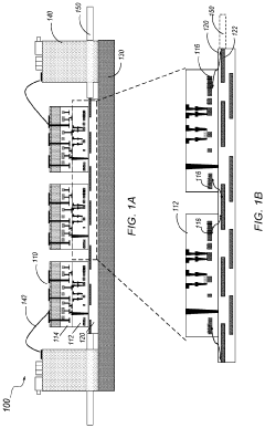
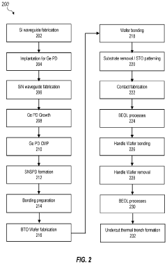
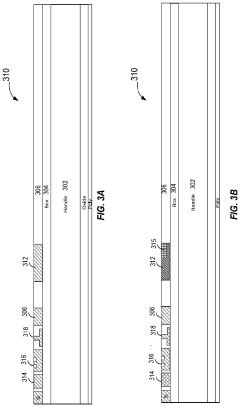
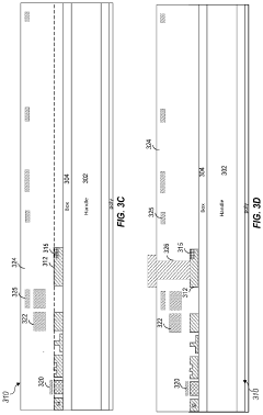
Method and structure to incorporate multiple low loss photonic circuit components
PatentPendingUS20230366913A1
Innovation
- A photonic integrated circuit (PIC) is designed using semiconductor processing technology, incorporating silicon nitride waveguides, Pockels effect optical phase shifters, superconductive nanowire single photon detectors, and optical isolation structures, with components like BaTiO3 optical phase shifters and Ge photodiodes, and employing techniques like high-temperature annealing to reduce waveguide losses and integrate various components on a single wafer or die.
Photonic integrated circuit
PatentWO2022161965A1
Innovation
- A photonic integrated circuit with a reflection layer that deflects and/or scatters light from the waveguide core to an optoelectronic component in a different layer, improving coupling efficiency without the need for direct physical contact or close proximity, using a CMOS-compatible manufacturing process and a cladding material with spacer layers to separate the waveguide core from the optoelectronic component.
Manufacturing Processes and Scalability
The manufacturing processes for Photonic Integrated Circuits (PICs) represent a critical factor in their commercial viability and technological advancement. Currently, several fabrication approaches dominate the industry, each with distinct advantages and limitations. Silicon photonics leverages existing CMOS infrastructure, enabling high-volume production through established 200mm and 300mm wafer processes. This manufacturing compatibility with electronic integrated circuits provides significant cost advantages and integration possibilities, though challenges remain in coupling efficiency and optical loss.
Indium phosphide (InP) platforms offer superior active component capabilities, particularly for light generation, but face scalability challenges due to smaller wafer sizes (typically 3-4 inches) and more complex processing requirements. The manufacturing ecosystem for InP is less developed than silicon, resulting in higher production costs despite excellent optical performance characteristics.
Silicon nitride (SiN) has emerged as a promising middle-ground platform, offering lower optical losses than silicon while maintaining compatibility with CMOS fabrication facilities. This material system enables passive components with exceptional performance, though integration with active elements requires hybrid approaches.
Scalability remains a fundamental challenge across all PIC platforms. The transition from laboratory prototypes to high-volume manufacturing encounters several bottlenecks, including process variability, yield management, and testing methodologies. Unlike electronic ICs, photonic circuits require specialized testing procedures that are difficult to parallelize, creating production bottlenecks. Current manufacturing processes typically achieve yields significantly lower than mature electronic IC processes, driving up costs and limiting mass-market adoption.
Packaging represents another critical manufacturing challenge. The precise alignment requirements for optical interfaces (typically sub-micron precision) necessitate specialized equipment and processes that are difficult to scale. Various approaches including edge coupling, grating couplers, and butt coupling each present different manufacturing trade-offs between coupling efficiency, bandwidth, and production complexity.
Recent advancements in manufacturing include the development of multi-project wafer (MPW) services, which allow multiple designs to share fabrication costs, and the emergence of foundry models similar to those in the electronic semiconductor industry. These developments are gradually reducing barriers to entry and enabling smaller organizations to prototype and produce PICs without massive capital investments.
Standardization Efforts and Ecosystem Development
The standardization of Photonic Integrated Circuits (PICs) represents a critical milestone in the maturation of this technology. Industry-wide standardization efforts have been gaining momentum, with organizations like the Photonic Integration Technology Center (PITC), IEEE, and the Optical Internetworking Forum (OIF) developing frameworks for component specifications, testing methodologies, and interface protocols. These standards are essential for ensuring interoperability between different PIC platforms and facilitating broader adoption across industries.
Process Design Kits (PDKs) have emerged as a cornerstone of the PIC ecosystem, providing designers with standardized libraries of photonic components that can be reliably manufactured. Leading foundries such as AIM Photonics, IMEC, and LioniX International have developed comprehensive PDKs that include validated component models, design rules, and verification tools. This standardization of the design process has significantly lowered the barrier to entry for new players in the PIC space.
Multi-Project Wafer (MPW) services represent another crucial development in the PIC ecosystem, allowing multiple designs to share fabrication costs on a single wafer run. These services have democratized access to advanced photonic fabrication capabilities, enabling smaller companies and academic institutions to prototype their designs without prohibitive investment. The establishment of regular MPW schedules by major foundries has created predictable development cycles for the industry.
Supply chain development has paralleled standardization efforts, with specialized providers emerging for packaging, testing, and assembly of PICs. The creation of this supporting ecosystem has addressed critical challenges in coupling light into and out of chips, thermal management, and electronic-photonic integration. Companies like Tyndall National Institute and ficonTEC have developed automated assembly solutions specifically tailored for photonic components.
Educational initiatives and workforce development programs have also become integral to the PIC ecosystem. Universities and industry consortia are establishing specialized curricula and training programs to address the skills gap in photonic design and manufacturing. Organizations like AIM Photonics Academy and the European Photonics Industry Consortium (EPIC) are leading efforts to build a qualified workforce capable of supporting the growing PIC industry.
Open-source design tools and platforms are gaining traction within the community, fostering collaboration and accelerating innovation. Projects like IPKISS, Luceda, and KLayout provide accessible entry points for new designers while establishing common design methodologies. These collaborative approaches to tool development complement formal standardization efforts and help establish de facto standards within the industry.
Unlock deeper insights with Patsnap Eureka Quick Research — get a full tech report to explore trends and direct your research. Try now!
Generate Your Research Report Instantly with AI Agent
Supercharge your innovation with Patsnap Eureka AI Agent Platform!