Photonic Integrated Circuits in Next-Gen Satellite Technologies
SEP 29, 20259 MIN READ
Generate Your Research Report Instantly with AI Agent
Patsnap Eureka helps you evaluate technical feasibility & market potential.
PIC Evolution and Satellite Integration Goals
Photonic Integrated Circuits (PICs) represent a revolutionary advancement in the field of optoelectronics, evolving from discrete optical components to highly integrated systems on a single chip. This evolution began in the 1980s with simple waveguide structures and has progressed to complex systems incorporating multiple optical functions. The miniaturization and integration capabilities of PICs have followed a trajectory similar to electronic integrated circuits, albeit at a different pace and with unique challenges related to light manipulation at the microscale.
The development of PICs has been marked by significant milestones, including the introduction of silicon photonics in the early 2000s, which leveraged existing semiconductor manufacturing infrastructure to produce optical components. This breakthrough dramatically reduced costs and increased production scalability. Subsequently, the integration of III-V materials with silicon platforms enabled active components such as lasers and amplifiers, expanding PIC functionality and application scope.
In the context of satellite technologies, PICs offer transformative potential by addressing critical limitations of traditional satellite systems. The primary integration goals focus on size, weight, and power (SWaP) reduction – crucial parameters for space applications where launch costs are directly proportional to payload mass. PICs can potentially reduce the footprint of optical communication systems by orders of magnitude while simultaneously improving performance metrics.
Another key integration goal involves enhancing satellite communication capabilities through wavelength division multiplexing (WDM) and coherent optical communication techniques implemented on photonic chips. These advancements aim to increase data throughput from megabits to terabits per second, revolutionizing space-based data transmission and enabling new applications such as high-resolution Earth observation and global broadband internet coverage.
Radiation hardness represents a significant technical objective for space-deployed PICs. The harsh radiation environment in space can cause performance degradation and failure in conventional photonic components. Therefore, developing radiation-resistant materials and designs for PICs is essential for ensuring long-term reliability in satellite operations.
The integration roadmap also encompasses the development of photonic-electronic convergence, where PICs and electronic integrated circuits are co-packaged or monolithically integrated to create complete systems-on-chip for satellite applications. This convergence aims to optimize signal processing, reduce interface losses, and further minimize power consumption.
Looking forward, the evolution of PICs for satellite applications is expected to focus on increasing functionality density, improving manufacturing yield, and developing standardized interfaces. The ultimate goal is to create modular, reconfigurable photonic systems that can adapt to changing mission requirements and extend satellite operational lifetimes through software-defined functionality.
Market Analysis for Space-Based Photonic Applications
The space-based photonic applications market is experiencing significant growth, driven by the increasing adoption of Photonic Integrated Circuits (PICs) in satellite technologies. Current market valuations indicate that the global space photonics market reached approximately $1.5 billion in 2022 and is projected to grow at a compound annual growth rate of 16.7% through 2030, potentially reaching $5.4 billion by the end of the decade.
Demand for space-based photonic applications is primarily fueled by the rapid expansion of satellite constellations for global communications networks. Companies like SpaceX, OneWeb, and Amazon's Project Kuiper are deploying thousands of satellites, creating substantial demand for high-performance, miniaturized optical communication systems. The market for inter-satellite optical links alone is expected to grow from $320 million in 2023 to over $1.2 billion by 2028.
Earth observation represents another significant market segment, with increasing requirements for hyperspectral imaging and remote sensing capabilities. This sector is projected to grow at 14.5% annually, driven by applications in climate monitoring, agriculture, and defense. Government space agencies worldwide are allocating larger portions of their budgets to photonics-based instruments, with NASA, ESA, and JAXA collectively investing over $800 million in photonic technologies for upcoming missions.
Commercial telecommunications providers represent the largest customer segment, accounting for approximately 42% of the total market. Government and military applications follow at 35%, with scientific research institutions comprising the remaining 23%. Geographically, North America leads with 38% market share, followed by Europe (29%), Asia-Pacific (24%), and rest of world (9%).
The market is witnessing a shift from traditional bulk optical components toward integrated photonic solutions, with PICs offering significant advantages in size, weight, power consumption, and radiation hardness. Industry analysts predict that by 2027, over 60% of new satellite optical payloads will incorporate some form of photonic integration.
Key market barriers include high initial development costs, with custom PIC development for space applications typically ranging from $5-15 million, and lengthy qualification cycles averaging 3-5 years for space-grade photonic components. Despite these challenges, venture capital investment in space photonics startups has surged, with over $1.2 billion invested since 2020.
The market outlook remains highly positive, with emerging applications in quantum communications, optical synthetic aperture radar, and space-based optical computing expected to create new revenue streams. As manufacturing volumes increase and standardization improves, costs are projected to decrease by 30-40% over the next five years, further accelerating market growth.
Current PIC Technology Limitations in Space Environment
Despite the promising advancements in Photonic Integrated Circuits (PICs) for satellite applications, several significant technical limitations persist when deploying these systems in the harsh space environment. Radiation exposure represents perhaps the most formidable challenge, as high-energy particles and cosmic radiation can induce both immediate performance degradation and long-term cumulative damage to photonic components. Silicon-based PICs are particularly vulnerable to displacement damage and ionization effects, which can alter refractive indices and increase propagation losses.
Thermal management presents another critical limitation. The extreme temperature fluctuations in space—ranging from -150°C to +150°C in low Earth orbit—place enormous stress on PIC materials. Current photonic platforms exhibit mismatched coefficients of thermal expansion between different integrated materials, leading to mechanical stress, delamination, and eventual device failure. Additionally, the absence of convective cooling in the vacuum of space necessitates sophisticated thermal dissipation strategies that current PIC packaging solutions struggle to provide.
Reliability and operational lifetime constraints further complicate PIC deployment in satellite systems. Space-grade qualification demands components that can function flawlessly for 10-15 years without maintenance, far exceeding typical terrestrial requirements. Present PIC manufacturing processes have not yet demonstrated the necessary consistency and defect control to meet these stringent reliability standards, with current failure rates remaining unacceptably high for mission-critical space applications.
Integration density limitations also impede the full potential of space-based PICs. While terrestrial applications benefit from increasingly miniaturized components, radiation hardening measures often necessitate larger feature sizes and redundant systems, reducing the integration density advantage that makes PICs attractive. The additional shielding and redundancy requirements can increase mass by 30-50%, directly conflicting with the satellite industry's push toward smaller, lighter platforms.
Power efficiency remains suboptimal for space deployment. Current laser sources and amplifiers integrated into PICs typically operate at 5-15% wall-plug efficiency, which is inadequate for power-constrained satellite platforms. Additionally, the coupling interfaces between electronic and photonic components introduce further losses that cannot be easily compensated in the limited power budget of satellite systems.
Manufacturing and testing protocols present practical barriers as well. The specialized equipment and cleanroom facilities required for PIC fabrication are not readily compatible with space-grade qualification processes. Current testing methodologies cannot fully simulate the combined effects of radiation, vacuum, and thermal cycling, leading to potential reliability gaps between ground testing and actual space performance.
Current PIC Solutions for Satellite Communications
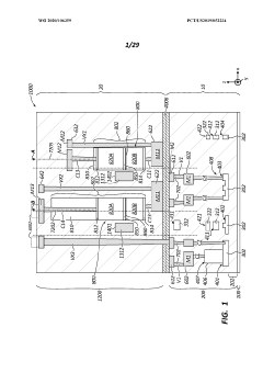
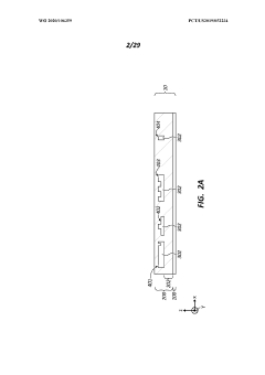
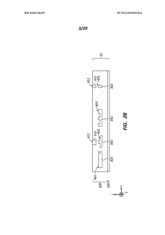
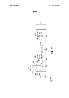
01 Integration of optical components on a single chip
Photonic integrated circuits (PICs) involve the integration of multiple optical components such as waveguides, modulators, detectors, and light sources on a single chip. This integration enables compact, high-performance optical systems with reduced size, weight, and power consumption compared to discrete optical components. The integration technology allows for complex optical functionalities while maintaining signal integrity and minimizing coupling losses between components.- Integration of optical components on a single chip: Photonic integrated circuits (PICs) involve the integration of multiple optical components such as waveguides, modulators, detectors, and light sources on a single chip. This integration enables compact, high-performance optical systems with reduced size, weight, and power consumption compared to discrete optical components. The integration technology allows for complex optical functionalities while maintaining signal integrity across the chip.
- Silicon photonics technology for PICs: Silicon photonics has emerged as a dominant platform for photonic integrated circuits due to its compatibility with CMOS manufacturing processes. This technology leverages existing semiconductor fabrication infrastructure to create optical devices on silicon substrates. Silicon photonics enables high-volume, low-cost production of PICs with high integration density and performance for applications in data communications, telecommunications, and sensing.
- Hybrid and heterogeneous integration approaches: Hybrid and heterogeneous integration approaches combine different material platforms to leverage their respective advantages in photonic integrated circuits. These methods include bonding III-V materials (for light sources) with silicon photonics, integrating lithium niobate for modulators, or incorporating other specialized materials for specific optical functions. These integration techniques overcome the limitations of single-material platforms and enable enhanced functionality in PICs.
- Advanced waveguide structures and optical interconnects: Advanced waveguide structures and optical interconnects form the backbone of photonic integrated circuits, enabling efficient light propagation and routing. These include strip waveguides, rib waveguides, slot waveguides, and photonic crystal waveguides with specialized geometries to control light propagation. Novel interconnect designs address challenges in coupling efficiency, polarization management, and minimizing optical losses at junctions and bends within the PIC.
- Integration of active and passive optical components: The integration of both active and passive optical components on photonic integrated circuits enables complete optical systems on a chip. Active components include lasers, modulators, and photodetectors that generate, manipulate, or detect light. Passive components include waveguides, splitters, couplers, and filters that route and process optical signals. The co-integration of these components requires specialized design approaches and fabrication techniques to ensure optimal performance and compatibility.
02 Silicon photonics manufacturing techniques
Silicon photonics leverages established semiconductor manufacturing processes to create photonic integrated circuits. These techniques include lithography, etching, deposition, and wafer bonding to fabricate optical structures on silicon substrates. The compatibility with CMOS fabrication enables high-volume, cost-effective production of PICs with nanometer-scale precision. Advanced manufacturing approaches allow for the integration of different materials to optimize optical performance while maintaining compatibility with electronic integration.Expand Specific Solutions03 Novel waveguide structures and designs
Advanced waveguide structures are fundamental to photonic integrated circuits, enabling efficient light propagation and manipulation. These include strip waveguides, rib waveguides, slot waveguides, and photonic crystal waveguides, each offering specific advantages for different applications. Novel designs focus on minimizing propagation losses, controlling dispersion, enhancing mode confinement, and enabling efficient coupling between different optical components. These structures are critical for signal routing, filtering, and processing in integrated photonic systems.Expand Specific Solutions04 Integration of active and passive optical components
Modern photonic integrated circuits combine both active components (lasers, modulators, detectors) and passive components (waveguides, splitters, filters) on the same platform. This heterogeneous integration often involves different material systems such as III-V semiconductors for light generation and silicon for passive routing. Advanced techniques include direct bonding, epitaxial growth, and transfer printing to achieve optimal performance of each component type while maintaining efficient interfaces between them. This integration is crucial for creating complete optical systems on a chip.Expand Specific Solutions05 Applications in optical communications and sensing
Photonic integrated circuits enable breakthrough applications in optical communications, sensing, and computing. In telecommunications, PICs support high-bandwidth transceivers for data centers and long-haul communications with advanced modulation formats. For sensing applications, integrated photonics enables compact, sensitive devices for environmental monitoring, biomedical diagnostics, and LiDAR systems. Emerging applications include quantum information processing, neuromorphic computing, and microwave photonics, where the precise control of light on-chip offers unique advantages over electronic solutions.Expand Specific Solutions
Leading Companies in Space Photonics Ecosystem
The photonic integrated circuits (PICs) market in next-generation satellite technologies is in its growth phase, with an expanding market driven by increasing demand for high-bandwidth satellite communications. The competitive landscape features established semiconductor giants like TSMC and Intel alongside specialized photonics innovators such as Rockley Photonics, EFFECT Photonics, and Lightmatter. Research institutions including Ghent University, IMEC, and University of California are advancing fundamental technologies, while defense contractors like BAE Systems and Honeywell are developing specialized applications. Technical maturity varies across applications, with telecommunications PICs being more advanced than quantum photonics solutions from companies like PsiQuantum. The industry is witnessing increased collaboration between academic institutions and commercial entities to overcome integration challenges and scale manufacturing capabilities.
Intel Corp.
Technical Solution: Intel has developed advanced Photonic Integrated Circuits (PICs) specifically designed for satellite communications through their Silicon Photonics technology platform. Their approach integrates optical components (lasers, modulators, detectors) onto silicon substrates using CMOS-compatible processes, enabling high-bandwidth data transmission for satellite networks. Intel's PICs feature wavelength division multiplexing (WDM) capabilities that allow multiple data streams to be transmitted simultaneously on different wavelengths, significantly increasing bandwidth capacity for satellite communications. Their technology achieves data rates exceeding 100 Gbps per optical channel while maintaining low power consumption (approximately 5 pJ/bit), critical for space applications where power resources are limited. Intel has also implemented radiation-hardened designs to protect their photonic circuits from the harsh space environment, incorporating redundancy mechanisms and specialized packaging techniques to ensure reliability in orbit.
Strengths: Intel leverages extensive semiconductor manufacturing expertise to produce highly integrated, reliable PICs at scale. Their CMOS-compatible processes enable cost-effective production compared to traditional discrete optical components. Weaknesses: Their silicon photonics platform may face challenges with thermal management in extreme space environments, and the technology requires specialized packaging solutions to maintain alignment precision in launch and orbital conditions.
Honeywell International Technologies Ltd.
Technical Solution: Honeywell has pioneered radiation-hardened Photonic Integrated Circuits specifically engineered for satellite applications, focusing on inertial navigation and quantum sensing capabilities. Their proprietary PIC platform integrates multiple optical functions including gyroscopes, accelerometers, and timing references onto a single chip, providing precise positioning data for satellites without relying on external signals. Honeywell's technology employs silicon nitride (SiN) waveguides that offer superior performance in radiation environments compared to traditional silicon photonics, with demonstrated radiation tolerance up to 100 krad total ionizing dose. Their PICs incorporate on-chip laser sources operating in the 1550nm band, achieving phase noise performance below -140 dBc/Hz at 1 kHz offset, enabling ultra-precise timing and sensing applications. The company has also developed specialized packaging techniques that maintain optical alignment during the extreme temperature fluctuations (-40°C to +85°C) experienced in space environments, with demonstrated stability better than 0.1 dB over the full temperature range.
Strengths: Honeywell's extensive aerospace heritage provides deep understanding of space qualification requirements, resulting in highly reliable PICs designed specifically for the harsh space environment. Their integrated sensing capabilities offer unique advantages for satellite positioning and navigation. Weaknesses: Their specialized approach may result in higher production costs compared to commercial photonics platforms, and their focus on sensing applications may limit bandwidth capabilities for high-throughput communications applications.
Key Patents in Space-Grade Photonic Integration
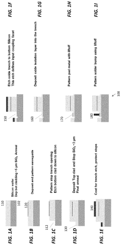
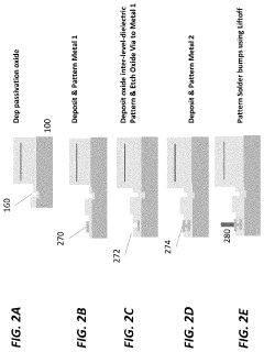
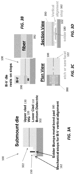
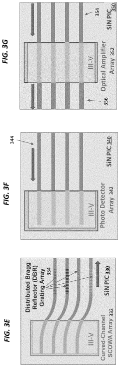
Hybrid integration for photonic integrated circuits
PatentActiveUS11340400B2
Innovation
- Hybrid integration techniques that allow coupling of light between silicon PICs and photonic devices from III-V or II-VI materials using silicon oxide claddings, trenches, and pedestals for precise alignment and electrical connection, enabling the integration of light sources, lasers, and optical amplifiers.
Photonics optoelectrical system
PatentWO2020106359A1
Innovation
- A method involving the integration of photonics devices and laser stack structures within a common photonics dielectric stack, allowing for precision alignment and bonding using a fusion bond layer, thereby eliminating the need for additional packaging technologies.
Space Qualification Standards for Photonic Components
The integration of Photonic Integrated Circuits (PICs) into next-generation satellite technologies necessitates rigorous space qualification standards to ensure reliability in the harsh space environment. These standards are primarily governed by organizations such as NASA, ESA, and JAXA, which have established comprehensive frameworks for qualifying photonic components for space applications.
Space qualification for photonic components involves testing against extreme temperature variations, ranging from -170°C to +125°C, which significantly exceed the typical commercial temperature ranges of -40°C to +85°C. These thermal cycling tests evaluate the component's ability to withstand rapid temperature fluctuations encountered during orbital transitions between sunlight and shadow.
Radiation hardness testing represents another critical aspect of space qualification standards. Photonic components must demonstrate resilience against Total Ionizing Dose (TID), Single Event Effects (SEE), and displacement damage. Current standards typically require components to withstand radiation doses between 30 krad and 100 krad, depending on the mission profile and orbital parameters.
Vacuum compatibility testing evaluates component performance in the near-perfect vacuum of space, focusing on outgassing characteristics. The ASTM E595 standard specifies acceptable limits for Total Mass Loss (TML) at less than 1.0% and Collected Volatile Condensable Materials (CVCM) below 0.1%. These parameters are crucial for preventing contamination of sensitive optical surfaces and ensuring long-term reliability.
Mechanical qualification standards address vibration and shock resistance, simulating launch conditions where components may experience forces exceeding 20g. Random vibration testing across frequencies from 20 Hz to 2000 Hz and pyrotechnic shock testing up to 10,000g are commonly required to validate structural integrity.
Reliability standards for space-grade photonic components typically demand failure rates below 100 FIT (failures in 10^9 hours) and operational lifetimes exceeding 15 years without maintenance. This necessitates accelerated life testing methodologies specific to photonic technologies, including high-temperature operating life (HTOL) tests and highly accelerated stress testing (HAST).
The qualification process also encompasses specialized standards for optical performance stability under space conditions, including wavelength drift specifications typically below 0.1nm across the operational temperature range. Power consumption limitations are particularly stringent for satellite applications, with efficiency requirements often exceeding those of terrestrial applications by 30-50%.
Recent developments in qualification standards have begun addressing the unique challenges of integrated photonic circuits, moving beyond standards originally developed for discrete optical components. These emerging standards incorporate considerations for waveguide stability, coupling efficiency maintenance, and multi-channel crosstalk under space environmental stressors.
SWaP Optimization Strategies for Satellite PICs
Size, Weight, and Power (SWaP) optimization represents a critical frontier in the development of Photonic Integrated Circuits (PICs) for satellite applications. Current satellite PIC implementations face significant constraints due to the harsh space environment and limited resources available on spacecraft platforms. Traditional electronic components require substantial power, contribute significant weight, and occupy valuable space—all premium resources in satellite design.
The miniaturization potential of PICs offers transformative advantages for satellite systems. By integrating multiple optical functions onto a single chip, PICs can reduce component count by 60-80% compared to discrete optical systems. This integration directly translates to weight reductions of up to 75% for equivalent functionality, while simultaneously decreasing power consumption by 30-50% through reduced optical coupling losses and more efficient thermal management.
Material selection plays a crucial role in SWaP optimization. Silicon photonics provides excellent integration density but faces radiation hardness challenges. Alternatively, indium phosphide (InP) platforms offer superior radiation tolerance and direct light emission capabilities, though with lower integration density. Emerging silicon nitride (SiN) platforms present a promising middle ground, combining moderate integration density with excellent radiation performance and lower propagation losses.
Novel packaging approaches further enhance SWaP metrics. Three-dimensional integration techniques, where electronic and photonic layers are vertically stacked, can reduce footprint by up to 65% compared to side-by-side integration. Hermetic packaging solutions utilizing advanced materials like silicon carbide offer superior thermal management while maintaining the stringent vacuum and contamination requirements of space environments.
Power optimization strategies include the implementation of passive optical components where possible, reducing the need for power-hungry active elements. When active components are necessary, the development of high-efficiency laser sources and detectors specifically designed for space applications can reduce power requirements by 40-60% compared to terrestrial equivalents.
Thermal management represents another critical aspect of SWaP optimization. Advanced thermal simulation techniques during the design phase, coupled with innovative heat dissipation structures integrated directly into PIC packages, can improve thermal efficiency by 25-35%, allowing for higher component density without compromising reliability or lifetime in the vacuum environment of space.
Unlock deeper insights with Patsnap Eureka Quick Research — get a full tech report to explore trends and direct your research. Try now!
Generate Your Research Report Instantly with AI Agent
Supercharge your innovation with Patsnap Eureka AI Agent Platform!