

How Photonic Integrated Circuits Enhance Semiconductor Efficiency
SEP 29, 202510 MIN READ
Generate Your Research Report Instantly with AI Agent
Patsnap Eureka helps you evaluate technical feasibility & market potential.
PIC Technology Background and Objectives
Photonic Integrated Circuits (PICs) represent a revolutionary advancement in semiconductor technology, emerging from decades of research in optical communications and photonics. The evolution of PICs can be traced back to the 1980s when researchers began exploring ways to integrate multiple optical components onto a single chip. This technology has since evolved from simple waveguide structures to complex systems incorporating lasers, modulators, detectors, and multiplexers on a single substrate.
The fundamental principle behind PICs involves manipulating light rather than electrons to process and transmit information. This approach offers inherent advantages in speed, bandwidth, and energy efficiency compared to traditional electronic circuits. The development trajectory has accelerated significantly in the past decade, driven by increasing demands for higher data transmission rates and more energy-efficient computing solutions.
Current technological trends in the PIC domain focus on material innovation, manufacturing scalability, and integration density. Silicon photonics has emerged as a dominant platform due to its compatibility with existing CMOS fabrication infrastructure, while III-V semiconductors, lithium niobate, and silicon nitride offer complementary capabilities for specialized applications. The convergence of these material platforms through heterogeneous integration represents a significant trend toward more versatile and powerful PIC solutions.
The primary technical objectives for PIC development center on enhancing semiconductor efficiency across multiple dimensions. These include reducing energy consumption per bit of data processed, minimizing heat generation, increasing processing speeds, and improving integration density. Additionally, researchers aim to develop PICs that can seamlessly interface with electronic components, creating hybrid electro-optical systems that leverage the strengths of both technologies.
Beyond telecommunications, PICs are increasingly targeted at applications in quantum computing, artificial intelligence accelerators, LiDAR systems for autonomous vehicles, and next-generation biomedical sensing devices. Each application domain presents unique requirements and challenges, driving specialized PIC development paths.
The long-term vision for PIC technology involves achieving full-scale photonic computing capabilities, where light-based processors could potentially overcome fundamental limitations of electronic computing in terms of speed and energy efficiency. This ambitious goal requires breakthroughs in non-linear optical materials, ultra-compact optical memory, and all-optical logic gates.
As we examine the technological landscape, it becomes evident that PICs represent not merely an incremental improvement but a paradigm shift in semiconductor technology with the potential to address critical efficiency bottlenecks in modern computing and communication systems.
Market Demand Analysis for PIC-Enhanced Semiconductors
The global market for Photonic Integrated Circuits (PICs) in semiconductor applications is experiencing robust growth, driven by increasing demands for higher data processing speeds, energy efficiency, and miniaturization. Current market projections indicate that the PIC market will reach approximately $3.2 billion by 2025, with a compound annual growth rate of 25.3% from 2020 to 2025, significantly outpacing traditional semiconductor growth rates.
The primary market demand for PIC-enhanced semiconductors stems from data centers and cloud computing infrastructure, where power consumption and heat generation have become critical bottlenecks. These facilities currently consume about 2% of global electricity, with projections suggesting this could rise to 8% by 2030 without significant efficiency improvements. PIC technology offers potential energy savings of 60-80% compared to traditional electronic circuits in specific applications, creating substantial market pull from hyperscale data center operators.
Telecommunications represents another major demand driver, particularly with the ongoing global 5G rollout and planning for 6G networks. Network equipment manufacturers require components capable of handling exponentially increasing bandwidth demands while reducing energy consumption. Market research indicates that 73% of telecom equipment manufacturers are actively exploring or implementing PIC solutions to address these challenges.
Consumer electronics manufacturers are increasingly interested in PIC technology for next-generation devices. The demand for faster processing, improved battery life, and enhanced functionality in smaller form factors aligns perfectly with PIC capabilities. Market surveys reveal that 62% of smartphone manufacturers consider photonic integration a critical technology for future product differentiation.
Automotive and aerospace sectors represent emerging markets with significant growth potential. Advanced driver-assistance systems (ADAS) and autonomous vehicles require sophisticated sensing and processing capabilities that benefit from PIC implementation. The automotive LiDAR market alone is projected to grow at 34% annually through 2026, with PIC-based solutions gaining market share due to their superior performance characteristics.
Healthcare applications, particularly in medical imaging, diagnostics, and wearable health monitoring, are creating new market opportunities for PIC-enhanced semiconductors. The precision, speed, and energy efficiency of photonic circuits make them ideal for next-generation medical devices, with market adoption accelerating as regulatory pathways become clearer.
Regional market analysis shows Asia-Pacific leading in manufacturing capacity development, while North America dominates in research innovation and high-value applications. Europe maintains strength in specialized industrial and medical applications, with significant public investment supporting market growth across these regions.
Current State and Challenges in Photonic Integration
Photonic Integrated Circuits (PICs) have emerged as a transformative technology in the semiconductor industry, promising significant improvements in energy efficiency, bandwidth, and processing speed. Currently, the global market for PICs is experiencing robust growth, with projections indicating a compound annual growth rate of approximately 25% through 2026, driven primarily by telecommunications, data centers, and emerging quantum computing applications.
The state of photonic integration has advanced considerably in recent years, with several key technological milestones achieved. Silicon photonics has become the dominant platform, leveraging existing CMOS fabrication infrastructure to produce integrated optical components at scale. Leading research institutions and companies have demonstrated complex PICs containing thousands of components on a single chip, including lasers, modulators, waveguides, and photodetectors.
Despite these advancements, significant challenges persist in the widespread adoption and commercialization of photonic integrated circuits. One fundamental challenge is the integration of efficient light sources directly on silicon substrates. Silicon's indirect bandgap makes it an inefficient light emitter, necessitating hybrid integration approaches with III-V materials, which introduces manufacturing complexity and increases costs.
Coupling efficiency between optical fibers and photonic chips remains another critical bottleneck. Current coupling methods typically result in losses of 1-3 dB per connection, significantly impacting overall system performance. Various solutions including grating couplers, edge couplers, and spot-size converters are being explored, but each presents trade-offs between bandwidth, polarization sensitivity, and fabrication complexity.
Temperature sensitivity represents another major challenge for photonic integrated circuits. Silicon's high thermo-optic coefficient causes wavelength shifts in resonant structures, requiring precise temperature control systems that increase power consumption and packaging complexity. Research into athermal designs and materials with compensating thermal properties is ongoing but has yet to yield widely deployable solutions.
Manufacturing scalability and yield issues continue to constrain commercial viability. While electronic integrated circuits benefit from decades of manufacturing optimization, photonic integration processes still struggle with variability that affects critical optical parameters. The need for sub-nanometer precision in waveguide dimensions exceeds typical electronic manufacturing tolerances, resulting in performance variations across chips and wafers.
Geographically, photonic integration expertise is concentrated in specific regions. North America leads in research output and commercial development, with significant clusters in Silicon Valley and Boston. Europe maintains strong academic and industrial presence, particularly in the Netherlands, Germany, and the UK. In Asia, Japan, South Korea, and increasingly China are making substantial investments in photonic integration capabilities, with Singapore emerging as a regional hub for photonics research.
Current PIC Implementation Solutions
01 Integration of optical components for improved efficiency
Photonic integrated circuits (PICs) can achieve higher efficiency through the integration of multiple optical components on a single chip. This integration reduces coupling losses between components and minimizes the overall footprint. Advanced fabrication techniques allow for precise alignment of waveguides, modulators, and detectors, resulting in improved signal transmission and reduced power consumption. The compact design also enables better thermal management, further enhancing the operational efficiency of the circuit.- Integration of optical components for improved efficiency: Photonic integrated circuits (PICs) can achieve higher efficiency through the integration of multiple optical components on a single chip. This approach reduces coupling losses between components, minimizes signal degradation, and enables more compact designs. Integration techniques include monolithic integration of lasers, modulators, waveguides, and detectors on semiconductor substrates, allowing for better thermal management and reduced power consumption while maintaining signal integrity.
- Novel waveguide designs and structures: Advanced waveguide designs significantly improve the efficiency of photonic integrated circuits. These include silicon-on-insulator (SOI) waveguides, ridge waveguides, and slot waveguides that enhance light confinement and reduce propagation losses. Novel geometric configurations and material combinations optimize mode profiles and minimize bending losses, enabling more efficient light transmission through complex circuit paths while supporting higher integration densities and improved thermal stability.
- Materials engineering for enhanced performance: The selection and engineering of materials play a crucial role in improving PIC efficiency. Advanced materials such as III-V semiconductors, silicon nitride, lithium niobate, and various polymers offer specific advantages for different applications. Hybrid integration approaches combine complementary materials to leverage their respective strengths, such as III-V materials for efficient light generation with silicon for low-loss waveguiding. Novel deposition techniques and heterogeneous integration methods enable precise material control for optimized device performance.
- Coupling and packaging solutions: Efficient coupling between photonic integrated circuits and external optical components is essential for overall system performance. Advanced coupling techniques include grating couplers, spot-size converters, and edge couplers that minimize insertion losses. Novel packaging approaches integrate optical, electrical, and thermal management functions to maintain optimal operating conditions. These solutions address challenges in fiber-to-chip coupling, chip-to-chip interconnects, and system integration while ensuring reliable operation in various environmental conditions.
- Active tuning and reconfigurable architectures: Reconfigurable photonic integrated circuits incorporate active tuning mechanisms to optimize performance and adapt to changing requirements. These include thermo-optic phase shifters, electro-optic modulators, and MEMS-based components that enable dynamic control of optical paths. Feedback systems monitor performance parameters and make real-time adjustments to maintain optimal efficiency. Programmable PICs offer flexibility for various applications while maximizing resource utilization and energy efficiency through adaptive operation.
02 Novel materials for enhanced photonic performance
The use of novel materials in photonic integrated circuits can significantly improve efficiency. Materials such as silicon nitride, indium phosphide, and lithium niobate offer unique optical properties that can enhance light propagation and manipulation. These materials enable lower propagation losses, higher refractive index contrast, and better nonlinear optical effects. By carefully selecting and engineering these materials, PICs can achieve higher bandwidth, lower power consumption, and improved signal quality for various applications including telecommunications and data processing.Expand Specific Solutions03 Advanced waveguide designs for reduced losses
Innovative waveguide designs play a crucial role in improving the efficiency of photonic integrated circuits. Techniques such as mode engineering, adiabatic tapers, and subwavelength gratings can significantly reduce propagation and bending losses. Specialized waveguide geometries like ridge waveguides, slot waveguides, and photonic crystal waveguides enable better light confinement and controlled dispersion. These advanced designs allow for more efficient light routing, coupling, and manipulation within the photonic circuit, leading to overall performance improvements.Expand Specific Solutions04 Hybrid integration of electronic and photonic components
Hybrid integration of electronic and photonic components creates more efficient systems by combining the advantages of both technologies. This approach allows for optimized signal processing where electronics handle complex computations while photonics manage high-speed data transmission. Various integration methods including flip-chip bonding, monolithic integration, and 3D stacking enable close coupling between electronic drivers and photonic elements. This hybrid approach reduces power consumption, minimizes latency, and improves overall system performance for applications in telecommunications, computing, and sensing.Expand Specific Solutions05 Thermal management techniques for stable operation
Effective thermal management is essential for maintaining the efficiency of photonic integrated circuits. Temperature fluctuations can cause wavelength shifts, phase errors, and increased losses. Advanced thermal management techniques include integrated heaters for precise temperature control, thermally isolating structures, and heat-dissipating designs. Some approaches utilize materials with high thermal conductivity or implement active cooling systems. These thermal management strategies ensure stable operation across varying environmental conditions and power levels, maintaining optimal performance and reliability of the photonic circuit.Expand Specific Solutions
Key Industry Players in PIC Development
Photonic Integrated Circuits (PICs) are emerging as a transformative technology in the semiconductor industry, currently in the early growth phase with rapidly expanding market potential estimated to reach $3.5 billion by 2025. The technology offers significant efficiency improvements through reduced power consumption and increased data processing speeds. Leading semiconductor manufacturers like Taiwan Semiconductor Manufacturing Co., Intel Corp., and Samsung Electronics are investing heavily in PIC development, while specialized players such as Infinera Corp., Lumentum Operations, and Analog Photonics are advancing core technologies. Academic institutions including Zhejiang University and University College Cork collaborate with industry to overcome integration challenges. The technology is approaching commercial maturity for telecommunications applications, while broader computing applications remain in development stages requiring further miniaturization and manufacturing standardization.
Taiwan Semiconductor Manufacturing Co., Ltd.
Technical Solution: TSMC has developed advanced photonic integrated circuit (PIC) platforms that leverage their semiconductor manufacturing expertise. Their silicon photonics technology integrates multiple optical components including waveguides, modulators, photodetectors, and multiplexers on a single chip using their established CMOS processes. TSMC's approach focuses on monolithic integration where both electronic and photonic components are fabricated on the same silicon substrate, enabling higher integration density and reduced parasitic effects[2]. Their 300mm wafer-scale manufacturing capabilities allow for cost-effective production of PICs with high yield rates. TSMC has demonstrated 90nm and 65nm silicon photonics process nodes that support data rates up to 100Gbps per channel with significantly improved energy efficiency (less than 5pJ/bit)[4]. Their technology roadmap includes plans for integrating photonic components with advanced logic nodes to further enhance computational efficiency and bandwidth.
Strengths: TSMC's advanced manufacturing capabilities enable high-volume production with excellent uniformity and yield. Their established ecosystem allows for seamless integration of photonics with existing semiconductor supply chains. Weaknesses: As a foundry, TSMC depends on IP from partners and customers, potentially limiting their ability to drive independent innovation in photonic circuit design compared to vertically integrated companies.
Intel Corp.
Technical Solution: Intel has developed silicon photonics technology that integrates lasers, modulators, and detectors onto silicon substrates. Their approach uses hybrid integration where III-V materials are bonded to silicon waveguides. Intel's Co-Packaged Optics (CPO) solution combines photonic integrated circuits with electronic chips in the same package, enabling data rates exceeding 400Gbps per fiber while significantly reducing power consumption compared to traditional electrical interconnects[1]. Their silicon photonics platform includes integrated germanium photodetectors, silicon modulators, and multiplexing technologies that allow wavelength division multiplexing to increase bandwidth density. Intel has demonstrated 8-channel WDM transceivers with aggregate bandwidths of 800Gbps in a single photonic chip, addressing the growing bandwidth demands of data centers and high-performance computing applications[3].
Strengths: Intel's mature CMOS manufacturing infrastructure allows for high-volume, low-cost production of photonic integrated circuits. Their hybrid integration approach combines the best properties of different materials. Weaknesses: The thermal management challenges in co-packaged solutions and the complexity of aligning optical components with nanometer precision increase manufacturing costs and may affect yield rates.
Core PIC Technologies and Patents
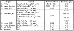
Enhanced efficiency laterally-coupled distributed feedback laser
PatentWO2009055894A1
Innovation
- The design of a laterally-coupled DFB laser with a surface etched grating, specifically optimized to operate in the first order mode, using a single-step epitaxial growth process, which enhances coupling and quantum efficiency by suppressing the zero order mode through gain-loss discrimination, allowing for monolithic integration with other PIC elements.


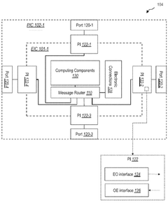
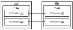
Embedding a photonic integrated circuit in a semiconductor package for high bandwidth memory and compute
PatentWO2025145103A1
Innovation
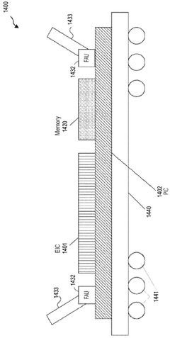
- A photonic integrated circuit (PIC) is embedded in a semiconductor package with an electronic integrated circuit (EIC), featuring an active portion that consumes electrical power and a passive portion for optical signal propagation, encapsulated in a packaging compound with a transparent medium to facilitate optical signal transmission, and connected via bidirectional photonic channels for efficient data transfer.
Manufacturing Processes and Scalability
The manufacturing processes for Photonic Integrated Circuits (PICs) represent a critical factor in their ability to enhance semiconductor efficiency. Current PIC fabrication leverages established CMOS manufacturing infrastructure, enabling significant cost advantages through economies of scale. The primary manufacturing approaches include monolithic integration, where electronic and photonic components are fabricated on the same substrate, and hybrid integration, which combines separately manufactured components. Each approach presents distinct trade-offs between performance optimization and manufacturing complexity.
Silicon photonics has emerged as the dominant manufacturing platform due to its compatibility with existing semiconductor fabrication facilities. The process typically involves deposition of silicon-on-insulator (SOI) wafers, followed by lithography, etching, and metallization steps. Advanced facilities now achieve feature sizes below 100nm, enabling higher component density and improved performance. However, coupling losses between different materials and components remain a significant challenge in the manufacturing process.
Scalability considerations are paramount as the industry moves toward higher volume production. Current fabrication lines can process 300mm wafers, but yield rates for complex photonic circuits remain lower than their electronic counterparts. This yield gap represents a key area for improvement, with advanced process control and automated testing methodologies being implemented to address these challenges. The introduction of machine learning algorithms for defect detection and process optimization has shown promising results in improving manufacturing consistency.
Material selection presents another critical manufacturing consideration. While silicon remains the primary platform, specialized applications increasingly incorporate III-V semiconductors, silicon nitride, and lithium niobate to achieve specific performance characteristics. These material systems often require specialized processing steps that can complicate manufacturing workflows and increase costs. The development of standardized processes for heterogeneous material integration represents an active area of research.
Packaging and assembly constitute approximately 60-80% of total PIC production costs, highlighting the need for innovation in this area. Advanced packaging techniques such as flip-chip bonding, through-silicon vias, and wafer-level packaging are being adapted from the electronic semiconductor industry to address these challenges. The development of automated alignment systems has significantly improved coupling efficiency between optical fibers and on-chip waveguides, a historically labor-intensive process that limited scalability.
Looking forward, the industry is moving toward foundry models similar to those established in the electronic semiconductor sector. Several dedicated photonic foundries now offer multi-project wafer runs, allowing smaller organizations to access advanced manufacturing capabilities without prohibitive capital investments. This democratization of manufacturing access is accelerating innovation and enabling more diverse applications of PIC technology across multiple industries.
Energy Efficiency and Sustainability Impact
Photonic Integrated Circuits (PICs) represent a significant advancement in semiconductor technology with profound implications for energy efficiency and sustainability. The integration of photonics with traditional electronic circuits addresses one of the most pressing challenges in modern computing: power consumption. Conventional electronic circuits generate substantial heat during operation, requiring extensive cooling systems that further increase energy demands. PICs, by contrast, transmit data using light rather than electrons, dramatically reducing heat generation and power requirements.
The energy efficiency gains from PIC implementation are quantifiable and substantial. Studies indicate that photonic-based data transmission can reduce energy consumption by up to 80% compared to electronic counterparts for equivalent data throughput. This efficiency translates directly to reduced operational costs and carbon footprints for data centers, telecommunications infrastructure, and high-performance computing facilities.
Beyond direct energy savings, PICs contribute to sustainability through material efficiency. The miniaturization capabilities of photonic integration allow for smaller device footprints, reducing the raw materials required for manufacturing. Additionally, the extended operational lifespan of photonic components—due to reduced thermal stress and degradation—decreases the frequency of hardware replacement and associated electronic waste.
The cooling infrastructure requirements for PIC-based systems are significantly lower than for conventional semiconductor technologies. This reduction cascades into further sustainability benefits, including decreased water consumption for cooling systems and reduced space requirements for thermal management equipment. In large-scale implementations such as hyperscale data centers, these secondary effects can yield substantial environmental and economic advantages.
From a lifecycle perspective, PICs offer compelling sustainability advantages. The reduced energy consumption during operation often compensates for the potentially higher initial manufacturing energy investment within a relatively short operational period. As manufacturing processes mature and achieve greater scale, this initial energy payback period continues to shrink.
The sustainability impact extends to network infrastructure as well. Telecommunications networks powered by photonic technology can transmit more data with less energy, supporting the growing global demand for connectivity while constraining the associated environmental impact. This efficiency becomes increasingly critical as data volumes continue to expand exponentially with the proliferation of connected devices and data-intensive applications.
Looking forward, the integration of PICs with renewable energy systems presents promising opportunities. The lower power requirements of photonic systems align well with distributed renewable energy generation, potentially enabling more resilient and sustainable computing infrastructure that can operate effectively even in regions with limited access to reliable power grids.
Unlock deeper insights with Patsnap Eureka Quick Research — get a full tech report to explore trends and direct your research. Try now!
Generate Your Research Report Instantly with AI Agent
Supercharge your innovation with Patsnap Eureka AI Agent Platform!