

Patent Analysis in Photonic Integrated Circuits Development
SEP 29, 20259 MIN READ
Generate Your Research Report Instantly with AI Agent
PatSnap Eureka helps you evaluate technical feasibility & market potential.
PIC Technology Evolution and Objectives
Photonic Integrated Circuits (PICs) represent a revolutionary technology that integrates multiple photonic functions on a single chip, similar to electronic integrated circuits but utilizing light instead of electrons. The evolution of PIC technology can be traced back to the 1980s when the first basic photonic components were integrated. However, significant advancements only began to materialize in the early 2000s with improved fabrication techniques and materials science breakthroughs.
The technological trajectory of PICs has been characterized by increasing integration density, functionality, and performance. Initially limited to simple waveguides and basic components, modern PICs now incorporate complex systems including lasers, modulators, detectors, and multiplexers on a single substrate. This evolution has been driven by demands from telecommunications, data centers, and sensing applications requiring higher bandwidth, lower power consumption, and reduced footprint.
Patent analysis reveals several distinct phases in PIC development. The pioneering phase (1980s-1990s) focused on fundamental components and manufacturing processes. The consolidation phase (2000-2010) saw the emergence of standardized platforms and improved integration techniques. The current acceleration phase (2010-present) is characterized by commercialization efforts and application-specific developments, with patent filings increasing exponentially since 2015.
The primary objectives of current PIC technology development include achieving higher levels of integration while maintaining performance, developing standardized design and manufacturing processes, and reducing costs to enable mass-market adoption. Patent analysis indicates particular emphasis on novel materials integration, including silicon, indium phosphide, silicon nitride, and lithium niobate platforms, each offering distinct advantages for specific applications.
Another critical objective identified through patent trends is the development of hybrid integration technologies that combine different material platforms to leverage their respective strengths. This approach aims to overcome the limitations of individual materials and enable more versatile and powerful PIC solutions. Patents in this area have grown by approximately 300% in the last five years.
Looking forward, the technological roadmap for PICs aims to achieve seamless integration with electronic components (electronic-photonic co-integration), improved packaging solutions to address current coupling inefficiencies, and the development of automated design tools to simplify the creation of complex photonic circuits. Patent activity suggests that these objectives are driving significant research and development investments across both academic institutions and industry players.
Market Demand Analysis for Photonic Integration
The global market for Photonic Integrated Circuits (PICs) is experiencing robust growth, driven by increasing demand for high-speed data transmission, energy-efficient computing solutions, and advanced sensing technologies. Current market projections indicate the PIC market will reach approximately $3.5 billion by 2025, with a compound annual growth rate exceeding 25% between 2020-2025, significantly outpacing traditional electronic integrated circuits.
Telecommunications remains the primary driver for photonic integration, accounting for nearly 40% of market demand. The explosive growth in data center traffic, cloud computing, and 5G infrastructure deployment has created unprecedented bandwidth requirements that conventional electronic solutions cannot efficiently address. Major telecom operators and equipment manufacturers are actively seeking PIC-based solutions to enable higher data rates while reducing power consumption and physical footprint.
Data centers represent the fastest-growing segment for photonic integration, with demand increasing at approximately 30% annually. As hyperscale data centers expand globally, operators face critical challenges in managing power consumption and heat dissipation. Photonic interconnects offer up to 80% reduction in energy usage compared to electronic alternatives while enabling data rates exceeding 400 Gbps, making them increasingly essential for next-generation data center architectures.
The sensing and measurement sector is emerging as a significant market for PICs, particularly in medical diagnostics, environmental monitoring, and industrial automation. The market for PIC-based biosensors alone is projected to grow at 22% annually through 2025, driven by applications in point-of-care diagnostics and pharmaceutical research. The enhanced sensitivity and miniaturization capabilities of integrated photonics enable new classes of portable, high-precision sensing devices.
Automotive and aerospace industries are showing increasing interest in photonic integration for LiDAR systems, optical gyroscopes, and high-bandwidth vehicle networks. The automotive LiDAR market is expected to grow substantially as autonomous driving technologies mature, with integrated photonics offering pathways to reduce system cost and size while improving performance.
Regionally, North America currently leads in PIC market share at approximately 35%, followed by Europe and Asia-Pacific. However, Asia-Pacific, particularly China, is demonstrating the fastest growth rate, supported by substantial government investments in photonics infrastructure and manufacturing capabilities.
Customer requirements are evolving toward higher levels of integration, with growing demand for heterogeneous integration that combines multiple optical functions with electronic control on a single chip. Industry surveys indicate that over 70% of end-users prioritize reduced form factor and power consumption as critical adoption factors, while cost reduction remains essential for mass-market applications.
Global PIC Development Status and Challenges
Photonic Integrated Circuits (PICs) have emerged as a transformative technology in the field of optoelectronics, promising significant advantages in terms of size, power consumption, and performance compared to traditional electronic circuits. Currently, the global PIC development landscape shows considerable regional variations with distinct technological approaches and market focuses.
The United States maintains leadership in PIC research and commercialization, with significant investments from both government agencies like DARPA and major corporations such as Intel and Cisco. Silicon photonics dominates the U.S. approach, leveraging existing semiconductor manufacturing infrastructure. The U.S. patent landscape reveals concentrated efforts in data center applications and telecommunications, with a growing focus on quantum computing applications.
Europe presents a strong research ecosystem centered around photonic integration platforms. Organizations like IMEC in Belgium and Fraunhofer in Germany have established world-class photonics research facilities. The European patent portfolio demonstrates particular strength in III-V material integration and bio-photonic sensing applications, with significant public funding through programs like Horizon Europe supporting collaborative innovation.
Asia, particularly China, Japan, and Singapore, has rapidly accelerated PIC development activities. China's national initiatives have resulted in exponential growth in PIC-related patents over the past five years, focusing primarily on telecommunications applications. Japan maintains traditional strength in specialized materials and packaging solutions, while Singapore has positioned itself as a manufacturing hub for PIC technologies.
Despite significant progress, the PIC industry faces several critical challenges. Technical barriers include efficient light coupling between different photonic platforms, thermal management in dense photonic circuits, and standardization of design and manufacturing processes. The lack of established design automation tools comparable to those in the electronic industry significantly impedes development efficiency and increases costs.
Manufacturing scalability remains a persistent challenge, with current processes still requiring substantial customization. The integration of different material platforms (silicon, III-V semiconductors, lithium niobate) presents complex fabrication challenges that limit mass production capabilities. Testing and packaging account for approximately 60-80% of PIC production costs, creating a significant barrier to widespread commercial adoption.
The patent landscape analysis reveals increasing competition and potential for patent thickets in key application areas. Cross-licensing agreements between major players have become common, while smaller innovators face challenges in protecting their intellectual property against established corporations with extensive patent portfolios. This dynamic creates both opportunities for strategic partnerships and risks for emerging technology developers in the PIC ecosystem.
Current PIC Patent Landscape
01 Integration of optical components on a single chip
Photonic integrated circuits (PICs) involve the integration of multiple optical components such as waveguides, modulators, detectors, and light sources on a single chip. This integration enables compact, high-performance optical systems with reduced size, weight, and power consumption compared to discrete optical components. The integration technology allows for complex optical functionalities while maintaining signal integrity across the chip.- Integration of optical components on a single chip: Photonic integrated circuits (PICs) involve the integration of multiple optical components such as waveguides, modulators, detectors, and light sources on a single chip. This integration enables miniaturization of optical systems, reduces power consumption, and improves reliability by eliminating the need for multiple discrete components. The technology allows for complex optical functionalities to be performed within a compact footprint, making it suitable for various applications including telecommunications and data centers.
- Silicon photonics technology: Silicon photonics is a key technology platform for photonic integrated circuits that leverages existing CMOS manufacturing infrastructure. This approach uses silicon as the optical medium for guiding light, allowing for cost-effective mass production of PICs. Silicon photonics enables high-speed optical interconnects, efficient coupling between optical and electronic components, and integration with electronic circuits on the same substrate. The technology addresses challenges in optical signal processing and transmission for high-bandwidth applications.
- Novel waveguide structures and designs: Advanced waveguide structures are fundamental to photonic integrated circuits, enabling efficient light propagation and manipulation. These designs include strip waveguides, rib waveguides, slot waveguides, and photonic crystal waveguides with specific geometries to control light confinement and propagation characteristics. Novel waveguide designs address challenges such as polarization management, dispersion control, and minimizing propagation losses, which are critical for high-performance optical signal processing and transmission in integrated photonic platforms.
- Optical modulators and switches for PICs: Optical modulators and switches are essential components in photonic integrated circuits that control the amplitude, phase, or routing of light signals. These devices utilize various physical effects such as electro-optic, thermo-optic, or acousto-optic mechanisms to achieve high-speed modulation or switching functionality. Advanced designs focus on achieving low power consumption, high extinction ratio, compact footprint, and compatibility with standard fabrication processes, enabling efficient optical signal processing and routing in integrated photonic platforms.
- Integration of lasers and photodetectors: The integration of light sources (lasers) and photodetectors with passive optical components is crucial for creating fully functional photonic integrated circuits. This integration can be achieved through various methods including direct growth, bonding techniques, or hybrid integration approaches. Challenges include thermal management, coupling efficiency, and material compatibility. Advanced integration techniques enable complete optical systems on a single chip, supporting applications in optical communications, sensing, and computing while reducing size, power consumption, and manufacturing costs.
02 Silicon photonics technology for PICs
Silicon photonics technology leverages existing CMOS manufacturing infrastructure to create photonic integrated circuits. This approach uses silicon as the optical medium for waveguides and other photonic components, enabling cost-effective mass production of PICs. Silicon photonics facilitates the integration of electronic and photonic components on the same substrate, allowing for enhanced functionality and performance in data communication applications.Expand Specific Solutions03 Novel materials and structures for enhanced PIC performance
Advanced materials and innovative structures are being developed to enhance the performance of photonic integrated circuits. These include III-V semiconductor materials, thin-film lithium niobate, polymers, and hybrid integration approaches. Such materials enable improved light generation, modulation, and detection capabilities. Novel waveguide structures, resonators, and photonic crystals are also being implemented to control light propagation and enhance functionality within PICs.Expand Specific Solutions04 PIC applications in optical communications and data centers
Photonic integrated circuits are revolutionizing optical communications and data center interconnects by enabling high-bandwidth, energy-efficient data transmission. PICs support advanced modulation formats, wavelength division multiplexing, and coherent detection schemes needed for next-generation optical networks. These integrated solutions address the growing bandwidth demands while reducing power consumption in telecommunications infrastructure and data centers.Expand Specific Solutions05 Packaging and integration techniques for PICs
Advanced packaging and integration techniques are critical for connecting photonic integrated circuits to the outside world. These include fiber coupling methods, electronic-photonic co-packaging, and 3D integration approaches. Efficient optical I/O interfaces, thermal management solutions, and hermetic sealing techniques ensure reliable PIC operation in various environments. These packaging innovations enable PICs to be effectively deployed in practical applications while maintaining their performance advantages.Expand Specific Solutions
Key Industry Players in PIC Ecosystem
The photonic integrated circuits (PICs) market is currently in a growth phase, with an expanding ecosystem of players across semiconductor, telecommunications, and computing sectors. The market is projected to reach significant scale due to increasing demand for high-speed data transmission and energy-efficient computing solutions. Technologically, PICs are advancing from research to commercial applications, with varying maturity levels across different implementations. Leading semiconductor companies like Intel, TSMC, and Synopsys are investing heavily in PIC technology, while specialized players such as Lightmatter, Infinera, and Shanghai Xizhi are driving innovation in photonic computing and optical communications. Established telecommunications equipment providers including NXP, IBM, and Samsung are also entering the space, creating a competitive landscape that spans from foundational IP development to application-specific implementations.
Intel Corp.
Technical Solution: Intel has developed a comprehensive silicon photonics platform that integrates lasers, modulators, waveguides, and photodetectors on a single chip. Their technology enables data transmission rates exceeding 400 Gbps per fiber with plans to scale to terabit speeds[1]. Intel's approach focuses on hybrid integration, combining III-V materials for light generation with silicon for waveguiding and modulation. Their patented technology includes innovations in germanium-silicon photodetectors, which offer superior responsivity across the C-band spectrum[2]. Intel has also pioneered techniques for wafer-level testing of photonic integrated circuits (PICs), significantly reducing manufacturing costs. Their recent patents cover advanced multiplexing techniques that allow multiple wavelengths to be processed on a single chip, increasing bandwidth density[3].
Strengths: Mature manufacturing infrastructure leveraging existing CMOS facilities; vertical integration from design to fabrication; extensive patent portfolio covering fundamental PIC technologies. Weaknesses: Higher power consumption compared to specialized photonics companies; challenges in thermal management of hybrid integrated devices; relatively higher cost structure for low-volume applications.
Taiwan Semiconductor Manufacturing Co., Ltd.
Technical Solution: TSMC has developed an advanced silicon photonics platform that integrates with their industry-leading semiconductor manufacturing processes. Their technology enables the production of high-performance photonic integrated circuits on 300mm wafers using existing CMOS infrastructure, significantly reducing production costs[1]. TSMC's patented innovations include specialized processes for integrating germanium photodetectors with silicon waveguides, achieving responsivity exceeding 1A/W across the C-band spectrum. Their silicon photonics platform features low-loss waveguides (<0.5dB/cm) and high-speed modulators operating at 50+ Gbaud[2]. TSMC has also developed proprietary techniques for passive alignment of optical fibers to photonic chips, reducing packaging costs which traditionally account for up to 80% of PIC production expenses. Recent patents reveal advancements in heterogeneous integration methods that combine III-V materials with silicon photonics, enabling on-chip light sources while maintaining CMOS compatibility[3]. Their manufacturing approach emphasizes scalability and yield optimization, leveraging decades of semiconductor fabrication expertise.
Strengths: Unparalleled semiconductor manufacturing infrastructure and process control; ability to leverage existing CMOS ecosystem; economies of scale that reduce production costs. Weaknesses: Less vertical integration in photonics system design compared to specialized competitors; relatively newer entrant to photonics-specific patent landscape; dependence on partners for certain specialized photonic components.
Core Patent Analysis and Technical Innovations
Photonics Integrated Circuit Architecture
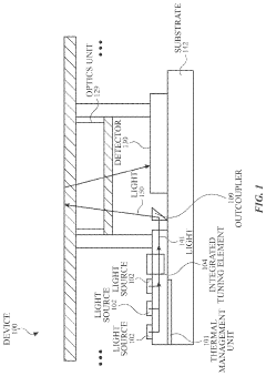
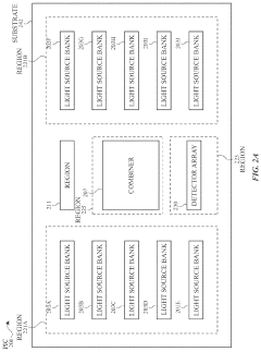
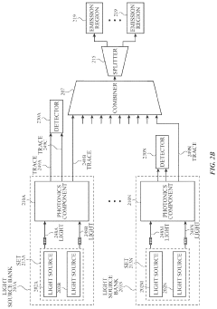
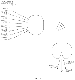
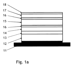
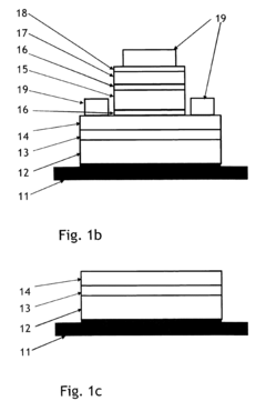
PatentActiveUS20230107907A1
Innovation
- The layout of a photonics integrated circuit (PIC) includes a plurality of optical components such as light sources, a detector array, and a combiner, with specific routing of optical traces to minimize optical losses and enable precise wavelength stabilization, utilizing multi-taps for signal crossing and reduction of losses.
A photonic integrated circuit and method of manufacturing the photonic integrated circuit
PatentInactiveEP2251722A1
Innovation
- A monolithic dual-polarization coherent receiver photonic integrated circuit (PIC) is developed using a single epitaxial process, with a specific layer structure and manufacturing method that includes a passive core layer, n-type upper cladding, and a p-type layer with a refractive index difference less than 0.3 rad/µm, allowing for efficient dual-polarization detection and reduced manufacturing complexity.

IP Strategy for PIC Development
Intellectual property strategy is crucial for companies developing photonic integrated circuits (PICs) as it directly impacts competitive positioning and market access. A comprehensive IP strategy for PIC development should begin with systematic patent landscape analysis to identify white spaces and potential infringement risks. This analysis reveals that PIC patents have grown exponentially over the past decade, with key technology clusters forming around waveguide structures, optical coupling methods, and integration with electronic components.
For effective PIC development, companies should implement a multi-layered IP approach. The foundation layer should focus on securing fundamental architecture patents that protect core PIC designs and manufacturing processes. These cornerstone patents establish territorial rights in key markets and create barriers to entry for competitors. The second layer should target application-specific implementations, particularly in high-growth sectors like data communications, biosensing, and quantum computing.
Strategic patent filing requires careful geographical consideration. While the United States remains the primary patent jurisdiction for PIC technologies, China has emerged as the fastest-growing region for photonics patents, with filing rates increasing by approximately 25% annually. European filings, particularly in Germany and the Netherlands, continue to represent significant innovation hubs for specialized PIC applications.
Beyond patents, PIC developers should incorporate complementary IP protection mechanisms. Trade secrets are particularly valuable for manufacturing processes that are difficult to reverse-engineer, such as specialized etching techniques or proprietary material deposition methods. Trademark protection for branded PIC platforms can create additional market differentiation and customer loyalty.
Collaborative IP development through strategic partnerships presents another dimension of effective PIC IP strategy. Joint development agreements with academic institutions, research organizations, and complementary technology providers can accelerate innovation while distributing IP development costs. These collaborations should include clear IP ownership provisions and field-of-use limitations to prevent future disputes.
Finally, defensive publication strategies should be considered for incremental innovations that may not warrant full patent protection but should remain in the public domain to prevent competitors from obtaining exclusive rights. This balanced approach to IP protection optimizes R&D investment while maintaining freedom to operate in this rapidly evolving technology space.
Standards and Interoperability in PIC Technology
The standardization landscape in Photonic Integrated Circuits (PICs) remains fragmented despite significant technological advancements. Currently, several industry consortia and standards bodies are working to establish common frameworks for PIC design, manufacturing, and testing. Organizations such as the Photonic Integration Technology Center (PITC), American Institute for Manufacturing Integrated Photonics (AIM Photonics), and the European Photonics Industry Consortium (EPIC) have initiated efforts to develop standardized Process Design Kits (PDKs) that enable designers to create PICs using standardized building blocks.
Interoperability challenges persist across the PIC ecosystem, particularly at the interfaces between photonic and electronic components. Patent analysis reveals that major industry players are actively developing proprietary solutions for optical-electrical interfaces, creating potential barriers to seamless integration. Companies like Intel, Cisco, and Huawei hold significant patent portfolios addressing interoperability issues, with particular focus on standardized coupling techniques between fiber optics and photonic chips.
The Multi-Project Wafer (MPW) approach has emerged as a de facto standard for PIC prototyping, allowing multiple designs to share fabrication costs. Patent data indicates growing interest in standardized testing methodologies, with companies like Lumentum and II-VI investing heavily in automated testing solutions compatible with various PIC platforms. These developments suggest a gradual movement toward industry-wide testing standards that could accelerate commercialization.
Data exchange formats represent another critical standardization frontier. The OASIS Compact Model Coalition has begun work on standardized compact models for photonic components, while the Si2 OpenAccess Coalition is extending electronic design automation (EDA) standards to accommodate photonic elements. Patent filings in this area have increased by approximately 35% annually since 2018, highlighting the industry's recognition of interoperability as a key enabler for market growth.
Packaging standards remain particularly challenging due to the diverse requirements of different application domains. Telecommunications applications typically require different optical interfaces than datacom or sensing applications. Recent patent activity shows increased focus on standardized edge and surface coupling techniques that could work across multiple application domains, potentially resolving this fragmentation.
The emergence of open-source PIC design frameworks, such as IPKISS and Nazca, represents a community-driven approach to standardization. While these frameworks currently account for a small percentage of patent activity, they demonstrate growing interest in collaborative approaches to interoperability challenges. Industry analysts predict that standardization efforts will accelerate as the PIC market matures, with particular emphasis on interfaces between established electronic design flows and emerging photonic design methodologies.
Unlock deeper insights with PatSnap Eureka Quick Research — get a full tech report to explore trends and direct your research. Try now!
Generate Your Research Report Instantly with AI Agent
Supercharge your innovation with PatSnap Eureka AI Agent Platform!