Photonic Integrated Circuits: Emerging Technologies in Biophotonics
SEP 29, 202510 MIN READ
Generate Your Research Report Instantly with AI Agent
Patsnap Eureka helps you evaluate technical feasibility & market potential.
Biophotonic PIC Evolution and Objectives
Photonic Integrated Circuits (PICs) have evolved significantly over the past decades, transitioning from theoretical concepts to practical applications across various fields. In the realm of biophotonics, this evolution has been particularly transformative, enabling unprecedented capabilities in biological sensing, imaging, and therapeutic applications. The integration of photonic components onto a single chip has followed a trajectory similar to electronic integrated circuits, but with unique challenges related to light manipulation at the micro and nano scales.
The historical development of biophotonic PICs began in the 1980s with rudimentary waveguide structures, progressing through the 1990s with the introduction of more complex passive components. The early 2000s marked a significant turning point with the successful integration of active components such as lasers and detectors on silicon platforms, opening new possibilities for biological applications. By the 2010s, heterogeneous integration techniques allowed for combining different material platforms, crucial for addressing the diverse wavelength requirements in biophotonic applications.
Current technological trends in biophotonic PICs include miniaturization of components, increased integration density, and enhanced functionality through novel materials and structures. The push toward lab-on-a-chip devices has driven innovation in microfluidic integration with photonic circuits, enabling real-time analysis of biological samples with minimal reagent consumption. Additionally, advances in fabrication techniques have improved reproducibility and reduced costs, making these technologies more accessible for research and commercial applications.
The primary objectives for biophotonic PIC development center around several key areas. First, enhancing sensitivity and specificity for detecting biomarkers at increasingly lower concentrations, potentially reaching single-molecule detection capabilities. Second, improving multiplexing capabilities to simultaneously analyze multiple biomarkers or parameters from a single sample. Third, developing robust, portable systems that can function reliably in point-of-care settings outside traditional laboratory environments.
Looking forward, the field aims to bridge the gap between research prototypes and commercially viable products by addressing challenges in standardization, packaging, and system integration. There is also a growing focus on developing PICs capable of operating across broader spectral ranges, particularly in the mid-infrared region where many biological molecules have distinctive absorption signatures. The ultimate goal is to create fully integrated biophotonic systems that combine sensing, processing, and communication capabilities on a single chip, enabling real-time, in-situ biological analysis with unprecedented precision and accessibility.
The convergence of photonics with other emerging technologies such as artificial intelligence and synthetic biology presents exciting opportunities for novel applications in personalized medicine, environmental monitoring, and food safety. These interdisciplinary approaches are expected to drive the next wave of innovation in biophotonic PICs.
Market Analysis for Integrated Biophotonic Solutions
The global market for integrated biophotonic solutions is experiencing robust growth, driven by increasing applications in healthcare, life sciences, and environmental monitoring. Current market valuations indicate that the biophotonics sector reached approximately $50 billion in 2022, with projections suggesting a compound annual growth rate (CAGR) of 11-13% through 2030. Within this broader market, photonic integrated circuits (PICs) for biological applications represent a rapidly expanding segment, currently valued at around $5 billion and expected to grow at 15-17% annually.
Healthcare applications dominate the market landscape, accounting for nearly 45% of the total market share. This includes diagnostic imaging, biosensors, point-of-care testing, and minimally invasive surgical tools. The pharmaceutical and biotechnology research segment follows at approximately 30%, driven by demand for high-throughput screening, drug discovery platforms, and advanced microscopy techniques.
Regional analysis reveals North America currently leads the market with approximately 40% share, followed by Europe (30%) and Asia-Pacific (25%). However, the Asia-Pacific region is demonstrating the fastest growth rate at 16-18% annually, primarily due to increasing healthcare infrastructure investments in China, Japan, and India, coupled with expanding research capabilities.
End-user segmentation shows hospitals and clinical laboratories constitute the largest customer base (38%), followed by research institutions (27%), pharmaceutical companies (20%), and biotechnology firms (15%). This distribution highlights the critical role of healthcare delivery systems in driving market demand.
Key market drivers include aging populations in developed economies, rising prevalence of chronic diseases requiring advanced diagnostics, increasing demand for personalized medicine, and growing adoption of point-of-care testing. Additionally, technological advancements enabling miniaturization, improved sensitivity, and reduced costs are expanding the application scope of integrated biophotonic solutions.
Market challenges include high initial development and manufacturing costs, complex regulatory approval processes for medical applications, and the need for specialized expertise in both photonics and biological sciences. Integration challenges between photonic components and biological samples also present significant technical hurdles that impact market adoption rates.
Emerging opportunities exist in developing economies where healthcare infrastructure is expanding rapidly, as well as in novel application areas such as environmental monitoring, food safety testing, and wearable health devices. The convergence of biophotonics with artificial intelligence and machine learning is creating new market segments focused on automated diagnostics and predictive healthcare analytics.
Global PIC Biophotonics Landscape and Barriers
The global landscape of Photonic Integrated Circuits (PICs) in biophotonics reveals significant regional disparities in research focus, technological maturity, and commercial implementation. North America, particularly the United States, leads in both academic research and commercial applications, with major universities like MIT, Stanford, and Caltech driving innovation alongside corporate giants such as Intel and IBM investing heavily in PIC technologies for biosensing and medical diagnostics.
Europe maintains a strong position through coordinated research initiatives like Horizon Europe and specialized photonics clusters in countries including Germany, the Netherlands, and France. The European approach emphasizes collaborative ecosystems between academia, industry, and government, resulting in notable advancements in lab-on-chip applications and point-of-care diagnostics using PIC platforms.
The Asia-Pacific region demonstrates rapid growth, with China making substantial investments in photonics infrastructure and talent development. Japan and South Korea focus on high-precision manufacturing capabilities for PIC components, while Singapore has established itself as a hub for biophotonics research with applications in tropical disease diagnostics.
Despite this global progress, significant barriers impede wider adoption of PIC technologies in biophotonics. Technical challenges remain paramount, including the integration of diverse materials systems required for both photonic and biological functionality. Silicon photonics dominates commercial applications, but biological applications often require specialized materials like III-V semiconductors, lithium niobate, or polymers, creating complex fabrication challenges.
Standardization represents another critical barrier, as the lack of unified design rules, component libraries, and testing protocols hampers interoperability and increases development costs. Unlike the mature electronic integrated circuit ecosystem, PIC development for biophotonics still operates in relatively isolated technological silos.
Cost factors present substantial obstacles, particularly for clinical applications. Current fabrication processes require specialized facilities and equipment, driving high production costs that limit commercial viability for many potential applications. The absence of high-volume manufacturing capabilities specifically optimized for biophotonics applications further exacerbates this issue.
Regulatory hurdles also significantly impact market entry, especially for medical applications. The complex approval processes for novel diagnostic and therapeutic devices incorporating PIC technology create lengthy development cycles and increase investment risk. These regulatory pathways vary substantially across different global regions, further complicating international commercialization strategies.
Addressing these barriers requires coordinated international efforts to establish standards, develop specialized fabrication facilities, and create regulatory frameworks that balance innovation with safety requirements. Cross-disciplinary collaboration between photonics engineers, biologists, and medical professionals remains essential to overcome these challenges and realize the full potential of PIC technologies in biophotonics.
Current PIC Architectures for Biomedical Applications
01 Integration of optical components on a single chip
Photonic integrated circuits (PICs) involve the integration of multiple optical components such as waveguides, modulators, detectors, and light sources on a single chip. This integration enables compact, high-performance optical systems with reduced size, weight, and power consumption compared to discrete optical components. The integration technology allows for complex optical functionalities while maintaining signal integrity and minimizing optical losses at component interfaces.- Integration of optical components on a single chip: Photonic integrated circuits (PICs) involve the integration of multiple optical components such as waveguides, modulators, detectors, and light sources on a single chip. This integration enables compact, high-performance optical systems with reduced size, weight, and power consumption compared to discrete optical components. The integration technology allows for complex optical functionalities while maintaining signal integrity and minimizing coupling losses between components.
- Silicon photonics and material platforms: Various material platforms are used for photonic integrated circuits, with silicon photonics being particularly prominent due to its compatibility with CMOS manufacturing processes. Other materials include III-V semiconductors, silicon nitride, lithium niobate, and polymer-based platforms. Each material system offers different advantages in terms of optical properties, integration capabilities, and application-specific performance. Hybrid integration approaches combine different materials to leverage their respective strengths.
- Optical interconnects and data communication: Photonic integrated circuits enable high-speed optical interconnects for data communication applications, offering advantages such as high bandwidth, low latency, and reduced power consumption compared to electronic interconnects. These PICs incorporate components for signal generation, modulation, transmission, and detection to facilitate data transfer within and between computing systems. Advanced modulation formats and wavelength division multiplexing techniques are implemented to increase data throughput.
- Quantum photonics and specialized applications: Photonic integrated circuits are increasingly used for quantum information processing, sensing, and other specialized applications. Quantum photonic circuits manipulate single photons or entangled photon pairs for quantum computing, quantum key distribution, and quantum sensing. Other specialized applications include integrated optical gyroscopes, optical frequency combs for precision metrology, biomedical sensing platforms, and LIDAR systems for autonomous vehicles.
- Fabrication techniques and packaging: Advanced fabrication techniques are essential for producing photonic integrated circuits with high yield and performance. These include lithography processes, etching techniques, deposition methods, and planarization approaches tailored to optical waveguide structures. Packaging solutions address challenges in fiber-to-chip coupling, thermal management, and electronic-photonic integration. Novel approaches include 3D integration, wafer-level packaging, and automated assembly techniques to improve manufacturability and reduce costs.
02 Silicon photonics manufacturing techniques
Silicon photonics leverages established CMOS manufacturing processes to create photonic integrated circuits. This approach enables high-volume, cost-effective production of PICs using silicon as the primary optical material. Manufacturing techniques include lithography, etching, deposition, and wafer bonding to create waveguides, resonators, and other optical structures. These processes allow for precise dimensional control at nanometer scales, which is critical for maintaining optical performance and ensuring compatibility with electronic integration.Expand Specific Solutions03 Heterogeneous integration of materials
Heterogeneous integration combines different material platforms to leverage their complementary properties in photonic integrated circuits. This approach integrates materials like III-V semiconductors (for light emission), silicon (for passive components), and lithium niobate (for modulation) on a single chip. Techniques such as wafer bonding, epitaxial growth, and transfer printing enable the combination of these disparate materials to create high-performance PICs with enhanced functionality that would not be possible using a single material system.Expand Specific Solutions04 Optical interconnects for data communications
Photonic integrated circuits provide high-bandwidth, energy-efficient optical interconnects for data communications in computing systems and telecommunications networks. These optical interconnects use wavelength division multiplexing, high-speed modulators, and photodetectors to transmit and receive data at rates exceeding electronic interconnects. The integration of multiple optical channels on a single PIC enables parallel data transmission with reduced latency and power consumption, making them ideal for data centers, high-performance computing, and telecommunications applications.Expand Specific Solutions05 Programmable photonic circuits
Programmable photonic integrated circuits incorporate reconfigurable optical elements that can be dynamically controlled to implement different optical functions. These circuits use phase shifters, tunable couplers, and optical switches to manipulate light paths and create adaptable optical processing systems. The programmability enables a single PIC to perform multiple functions through software control, supporting applications in quantum computing, optical signal processing, and artificial intelligence. This approach provides flexibility similar to electronic FPGAs but for optical domain processing.Expand Specific Solutions
Leading Organizations in Biophotonic PIC Development
Photonic Integrated Circuits (PICs) in biophotonics are transitioning from early development to commercial growth phase, with the market expected to reach significant expansion in the next decade. The technology maturity varies across applications, with diagnostic and sensing solutions leading the way. Key players represent diverse technological approaches: established semiconductor giants like TSMC, Intel, and AMD bring manufacturing expertise; specialized photonics companies such as Rockley Photonics and Infinera focus on innovative PIC designs; while research institutions including Caltech, MIT, and Zhejiang University drive fundamental breakthroughs. The ecosystem is further strengthened by telecommunications leaders like Cisco and Nokia, who are leveraging PICs for next-generation biomedical applications, creating a competitive landscape balanced between established manufacturers and specialized innovators.
Intel Corp.
Technical Solution: Intel has leveraged its semiconductor manufacturing expertise to develop advanced silicon photonics platforms with applications in biophotonics. Their technology centers on highly integrated photonic circuits manufactured using their established 300mm wafer facilities, enabling cost-effective production at scale. Intel's silicon photonics platform features hybrid integration of III-V lasers with silicon waveguides, providing reliable light sources directly on chip. For biophotonic applications, Intel has developed specialized versions of their photonic integrated circuits incorporating sensing elements such as interferometers and resonators capable of detecting biological analytes with high sensitivity. Their platform includes integrated germanium photodetectors with exceptional responsivity across relevant wavelengths for biological sensing. Intel has also pioneered packaging solutions that enable robust interfaces between their photonic chips and biological samples, including specialized microfluidic attachments that maintain optical alignment while allowing sample delivery. Their manufacturing approach enables unprecedented levels of integration, with thousands of photonic components on a single chip.
Strengths: Unmatched manufacturing capabilities enabling high-volume, low-cost production; exceptional integration density; established supply chain and quality control processes. Weaknesses: Primary focus on communications rather than biological applications; less specialized expertise in biointerface chemistry compared to dedicated biophotonics companies; corporate priorities may shift based on market demands.
California Institute of Technology
Technical Solution: Caltech has pioneered significant advancements in biophotonic integrated circuits through their Nanophotonics and Biophotonics Laboratory. Their approach centers on developing ultra-compact photonic integrated circuits for biological sensing and imaging applications. Caltech researchers have created novel photonic crystal cavities and resonators with extremely high quality factors that enable single-molecule detection capabilities. Their technology incorporates innovative waveguide designs that minimize optical losses while maximizing light-matter interactions in biological samples. A key innovation is their development of integrated optofluidic systems that combine microfluidic channels directly with photonic waveguides on the same chip, allowing for precise sample handling and optical interrogation simultaneously. Caltech has also pioneered the use of inverse design algorithms to create photonic components with unprecedented functionality and efficiency for specific biophotonic applications, enabling capabilities not possible with conventional design approaches.
Strengths: Cutting-edge research with exceptional sensitivity for molecular detection; innovative integration of microfluidics with photonics; advanced computational design methods yielding optimized structures. Weaknesses: Many technologies remain in research phase rather than commercial products; complex fabrication requirements may limit immediate widespread adoption; higher costs associated with specialized manufacturing processes.
Breakthrough Patents in Integrated Biophotonics
Photonic integrated circuit (PIC) and method for making same
PatentInactiveUS6788721B2
Innovation
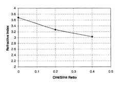
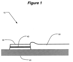
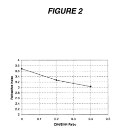
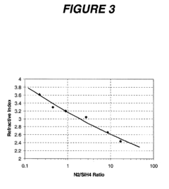
- The use of amorphous silicon (a-Si) materials, such as a-Si:H and a-Si:F based alloys, for waveguide formation in PICs, allowing for flexible index matching and low-loss coupling between active and passive components, achieved through Plasma Enhanced Chemical Vapor Deposition (PECVD) processes, which eliminates lattice match requirements and reduces optical absorption.
Heterogeneously integrated photonic platform with ingap layers
PatentPendingEP4462618A1
Innovation
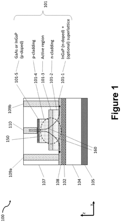
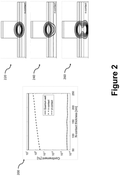
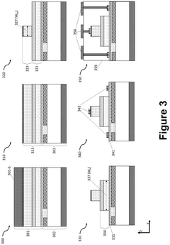
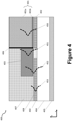
- The development of a heterogeneously integrated laser structure using butt-coupling and mode conversion with a detailed design that includes a high-bandgap InGaP contact layer and a dielectric waveguide structure, allowing for efficient coupling between active and passive waveguides, enabling high-yield bonding and robust semiconductor processing at short wavelengths.
Regulatory Framework for Biomedical Photonic Devices
The regulatory landscape for biomedical photonic devices represents a complex framework that varies significantly across global markets. In the United States, the Food and Drug Administration (FDA) classifies photonic integrated circuit (PIC) based medical devices primarily through the Center for Devices and Radiological Health (CDRH), with classification determined by risk level and intended use. Class II and Class III designations are common for biophotonic applications, requiring either 510(k) clearance or the more rigorous Premarket Approval (PMA) process.
The European Union has implemented the Medical Device Regulation (MDR) and In Vitro Diagnostic Regulation (IVDR), which introduced more stringent requirements for clinical evidence, post-market surveillance, and technical documentation for photonic medical technologies. These regulations emphasize the importance of risk management throughout the product lifecycle and require manufacturers to demonstrate clinical benefit against potential risks.
In Asia, regulatory frameworks show considerable variation. Japan's Pharmaceuticals and Medical Devices Agency (PMDA) has established specific pathways for novel photonic technologies, while China's National Medical Products Administration (NMPA) has recently updated its regulatory framework to accelerate approval for innovative medical technologies, including those based on photonic integration.
International standards play a crucial role in harmonizing these diverse regulatory requirements. ISO 13485 for quality management systems and IEC 60601 for electrical medical equipment safety provide foundational compliance frameworks. For biophotonic applications specifically, standards such as ISO 10993 for biocompatibility and IEC 62471 for photobiological safety are particularly relevant.
Emerging regulatory considerations for integrated photonic devices in biomedical applications include laser safety classifications, biocompatibility of materials in contact with biological tissues, and specific performance standards for optical coherence tomography, fluorescence imaging, and Raman spectroscopy applications. The miniaturization achieved through photonic integration introduces unique regulatory challenges regarding reliability, calibration stability, and long-term performance.
Data privacy and cybersecurity regulations have become increasingly important as photonic devices integrate with digital health ecosystems. The Health Insurance Portability and Accountability Act (HIPAA) in the US and the General Data Protection Regulation (GDPR) in Europe impose strict requirements on data handling for connected photonic diagnostic devices.
Regulatory pathways for combination products—where photonic devices incorporate pharmaceutical or biological components—present additional complexity, often requiring coordination between multiple regulatory divisions. This is particularly relevant for theranostic applications where photonic circuits enable both diagnostic and therapeutic functionalities.
Scalability and Manufacturing Challenges
The scaling of photonic integrated circuits (PICs) for biophotonic applications presents significant manufacturing challenges that must be addressed to enable widespread adoption. Current fabrication processes for PICs often rely on techniques borrowed from the semiconductor industry, which require adaptation for photonic components that operate at different scales and with different material requirements. The precision needed for waveguides, resonators, and other photonic elements demands nanometer-level accuracy, creating substantial yield challenges when scaling to high-volume production.
Material compatibility represents a critical hurdle in biophotonic PIC manufacturing. While silicon photonics offers excellent integration with CMOS processes, its limited transparency window restricts applications in certain biophotonic wavelength ranges. Alternative materials such as silicon nitride, indium phosphide, and lithium niobate provide better optical properties for biophotonics but introduce complex fabrication requirements and higher costs. The heterogeneous integration of these materials with sensing elements and microfluidic components further complicates manufacturing processes.
Packaging and interfacing challenges significantly impact scalability in biophotonic PICs. The precise alignment required between optical fibers and on-chip waveguides demands specialized equipment and processes that are difficult to automate cost-effectively. Additionally, the integration of electrical connections, temperature control elements, and microfluidic channels creates multi-domain packaging challenges that current manufacturing infrastructure struggles to address at scale.
Cost considerations remain paramount for commercial viability. Current fabrication approaches for high-performance biophotonic PICs often utilize expensive equipment and low-throughput processes. The transition from laboratory prototypes to commercial products requires significant investment in manufacturing technology development. While silicon photonics benefits from established semiconductor infrastructure, specialized biophotonic applications often require custom processes that have not achieved comparable economies of scale.
Standardization represents another significant challenge for the industry. Unlike electronic integrated circuits, photonic components lack widely accepted design rules, process design kits, and manufacturing standards. This fragmentation complicates supply chain development and increases costs as manufacturers must develop proprietary processes rather than leveraging industry standards. Recent initiatives by organizations such as AIM Photonics and PIXAPP aim to address these standardization gaps, but significant work remains to establish manufacturing ecosystems comparable to those in the electronic semiconductor industry.
Environmental control during manufacturing presents additional scaling challenges. Photonic devices are highly sensitive to contamination and process variations that can significantly impact optical performance. Maintaining the necessary clean room conditions and process consistency across high-volume production requires sophisticated monitoring and control systems that add complexity and cost to manufacturing operations.
Unlock deeper insights with Patsnap Eureka Quick Research — get a full tech report to explore trends and direct your research. Try now!
Generate Your Research Report Instantly with AI Agent
Supercharge your innovation with Patsnap Eureka AI Agent Platform!
