Patent Landscape of Photonic Integrated Circuits
SEP 29, 20259 MIN READ
Generate Your Research Report Instantly with AI Agent
Patsnap Eureka helps you evaluate technical feasibility & market potential.
PIC Technology Evolution and Objectives
Photonic Integrated Circuits (PICs) have evolved significantly since their conceptual inception in the 1960s, transforming from theoretical constructs to practical implementations that now power advanced telecommunications, data centers, and sensing applications. The evolution of PIC technology has been characterized by progressive miniaturization, increased functionality, and enhanced performance metrics, mirroring the development trajectory observed in electronic integrated circuits but with distinct challenges related to light manipulation at the microscale.
The initial development phase of PICs focused primarily on basic waveguide structures and simple optical functions. During the 1980s and early 1990s, research concentrated on fundamental building blocks such as waveguides, couplers, and basic modulators, primarily using III-V semiconductor materials like indium phosphide (InP). This period established the foundational technologies that would later enable more complex integration.
A significant technological shift occurred in the late 1990s and early 2000s with the emergence of silicon photonics, leveraging existing CMOS fabrication infrastructure to produce optical components on silicon substrates. This development dramatically reduced manufacturing costs and increased scalability potential, catalyzing accelerated research and commercial interest in the field. The compatibility with electronic integration pathways opened new possibilities for electro-optical systems on chip.
The past decade has witnessed remarkable advancements in PIC technology, characterized by increased integration density, expanded material platforms including silicon nitride and lithium niobate, and the development of hybrid integration approaches that combine the advantages of different material systems. These technological progressions have enabled PICs with hundreds or even thousands of components on a single chip, supporting complex functionalities previously requiring entire optical benches.
The primary objectives of current PIC technology development include achieving higher levels of integration while maintaining or improving performance, reducing power consumption, enhancing reliability, and developing standardized design and manufacturing processes. Additionally, there is significant focus on developing PICs capable of operating across broader wavelength ranges and supporting emerging applications in quantum computing, neuromorphic computing, and advanced sensing.
Patent landscapes in this domain reflect these evolutionary trends, with early patents focusing on basic components and fabrication methods, while more recent intellectual property emphasizes novel integration techniques, specialized applications, and manufacturing optimizations. The geographical distribution of patents has also evolved, initially concentrated in North America and Japan, but now showing significant activity in Europe and increasingly in China, reflecting the global recognition of PIC technology's strategic importance.
Market Demand Analysis for Photonic Integration
The global market for Photonic Integrated Circuits (PICs) is experiencing robust growth, driven primarily by increasing data traffic demands and the need for higher bandwidth communication systems. Current market valuations place the PIC sector at approximately 1.3 billion USD in 2023, with projections indicating a compound annual growth rate of 23% through 2030, potentially reaching 5.5 billion USD by the end of the decade.
Telecommunications remains the dominant application sector, accounting for nearly 40% of the current market share. This dominance stems from the critical role PICs play in enabling high-speed optical communication networks, coherent transmission systems, and next-generation 5G/6G infrastructure. Data centers represent the second-largest market segment, with rapidly increasing adoption rates as operators seek to address power consumption and data throughput challenges.
Consumer electronics applications are emerging as a significant growth vector, particularly in areas such as LiDAR for autonomous vehicles, AR/VR systems, and advanced sensing technologies. Market analysis indicates that this segment could grow at over 30% annually, outpacing the overall market average.
Regionally, North America currently leads market consumption at approximately 35% of global demand, followed closely by Asia-Pacific at 32%. However, the highest growth rates are being observed in China and other Asian manufacturing hubs, where substantial investments in photonic manufacturing infrastructure are being made.
Market demand is increasingly being shaped by several key factors. Energy efficiency has become paramount, with data centers and telecommunication providers seeking photonic solutions that can reduce power consumption by 60-80% compared to electronic alternatives. This trend aligns with global sustainability initiatives and regulatory pressures to reduce ICT carbon footprints.
Miniaturization represents another critical market driver, with end-users demanding smaller form factors that can be integrated into increasingly compact devices. This has accelerated interest in hybrid integration approaches that combine different material platforms.
Supply chain considerations have also emerged as a significant market factor following recent global disruptions. Customers are increasingly valuing manufacturing diversity and resilience, creating opportunities for new regional manufacturing clusters beyond traditional centers.
The market is further characterized by a growing demand for standardization and interoperability, as customers seek to avoid vendor lock-in and reduce integration costs. This has prompted industry consortia to develop common interfaces and design methodologies, potentially accelerating market adoption across multiple sectors.
Global PIC Development Status and Challenges
Photonic Integrated Circuits (PICs) have emerged as a transformative technology across global markets, yet their development status varies significantly by region. Currently, North America, Europe, and Asia-Pacific represent the primary hubs of PIC innovation, with each region demonstrating distinct technological strengths and market approaches.
In North America, particularly the United States, PIC development benefits from substantial private investment and strong academic-industrial partnerships. Companies like Intel, Cisco, and Infinera have established robust patent portfolios focusing on silicon photonics for data center applications. The region leads in commercialization efforts but faces challenges in scaling manufacturing processes for mass production.
European PIC development is characterized by strong governmental support through initiatives like Horizon Europe and PhotonDelta. The Netherlands, Germany, and the UK have created specialized photonics clusters that emphasize indium phosphide and silicon nitride platforms. While Europe excels in research innovation, it struggles with translating laboratory breakthroughs into commercial products at competitive price points.
The Asia-Pacific region, led by China, Japan, and Singapore, has rapidly accelerated PIC development through coordinated national strategies. China's investment in PIC technology has grown exponentially since 2015, with particular emphasis on telecommunications applications and quantum photonic integration. Japan maintains leadership in specialized materials and packaging solutions, while Singapore has positioned itself as a manufacturing hub.
Technical challenges persist across all regions. Integration density remains a significant limitation, with current commercial PICs typically containing fewer than 100 components—far below electronic integration levels. Coupling efficiency between different photonic elements continues to cause substantial signal losses, while packaging costs can represent up to 80% of total device expenses, hampering widespread adoption.
Standardization represents another critical challenge, as the industry lacks unified design rules, process design kits, and manufacturing protocols. This fragmentation slows development cycles and increases costs. Additionally, the talent gap in photonic engineering has become increasingly apparent, with universities struggling to produce graduates with the interdisciplinary skills required for advanced PIC development.
Environmental stability and reliability under varying operating conditions remain problematic for many PIC applications, particularly in harsh environments or space applications. Temperature sensitivity of photonic components often necessitates complex compensation mechanisms that increase system complexity and cost.
Despite these challenges, global patent filings for PIC technologies have grown at a compound annual rate exceeding 30% since 2010, indicating strong confidence in the technology's future potential across telecommunications, sensing, quantum computing, and biomedical applications.
Current PIC Patent Solutions and Approaches
01 Integration of optical components on a single chip
Photonic integrated circuits (PICs) involve the integration of multiple optical components such as waveguides, modulators, detectors, and light sources on a single chip. This integration enables miniaturization of optical systems while improving performance, reliability, and reducing power consumption. The technology allows for complex optical functionalities to be implemented in a compact form factor, making it suitable for various applications including telecommunications and data centers.- Integration of optical components on a single chip: Photonic integrated circuits (PICs) involve the integration of multiple optical components such as waveguides, modulators, detectors, and light sources on a single chip. This integration enables compact, high-performance optical systems with reduced size, weight, and power consumption compared to discrete optical components. The integration technology allows for complex optical functionalities while maintaining signal integrity and minimizing optical losses at component interfaces.
- Silicon photonics manufacturing techniques: Silicon photonics has emerged as a dominant platform for photonic integrated circuits due to its compatibility with CMOS manufacturing processes. These techniques leverage existing semiconductor fabrication infrastructure to create optical components on silicon substrates. Advanced manufacturing methods include lithography, etching, deposition, and wafer bonding to create waveguides, resonators, and other optical structures with nanometer-scale precision, enabling mass production of photonic integrated circuits with high yield and reliability.
- Optical interconnects for high-speed data transmission: Photonic integrated circuits are increasingly used for optical interconnects in high-speed data transmission applications. These interconnects utilize light instead of electrical signals to transfer data between chips, boards, or systems, offering advantages such as higher bandwidth, lower latency, and reduced power consumption. The integration of lasers, modulators, and photodetectors on a single chip enables efficient conversion between electrical and optical domains, supporting data rates from tens to hundreds of gigabits per second with minimal signal degradation over distance.
- Novel materials and structures for enhanced PIC performance: Research in photonic integrated circuits has expanded to include novel materials and structures beyond traditional silicon. These include III-V semiconductors, lithium niobate, polymers, and 2D materials that offer unique optical properties. Hybrid integration approaches combine different material platforms to leverage their respective advantages. Advanced structures such as photonic crystals, metamaterials, and subwavelength gratings are being incorporated to manipulate light propagation, enhance light-matter interaction, and enable new functionalities like nonlinear optics and quantum photonics on integrated platforms.
- Integration with electronic circuits and packaging solutions: The co-integration of photonic and electronic circuits represents a significant advancement in PIC technology. Various approaches include monolithic integration, where both electronic and photonic components are fabricated on the same substrate, and hybrid integration using techniques like flip-chip bonding. Advanced packaging solutions address challenges in fiber-to-chip coupling, thermal management, and electrical connections. These integrated electro-optic systems enable applications in telecommunications, data centers, sensing, and computing where both optical and electronic functionalities are required.
02 Silicon photonics technology
Silicon photonics is a key technology for photonic integrated circuits that leverages existing CMOS manufacturing infrastructure. By using silicon as the optical medium, these circuits can be fabricated using standard semiconductor processes, enabling cost-effective mass production. Silicon photonic integrated circuits can incorporate various optical elements including waveguides, resonators, and modulators to manipulate light signals for data transmission and processing applications.Expand Specific Solutions03 Hybrid integration of materials for enhanced functionality
Hybrid integration combines different materials such as III-V semiconductors with silicon to overcome the limitations of individual materials in photonic integrated circuits. This approach enables the integration of efficient light sources, amplifiers, and detectors with silicon waveguides. The hybrid integration techniques include wafer bonding, flip-chip bonding, and heterogeneous integration, allowing for optimized performance in various optical functions while maintaining compatibility with semiconductor manufacturing processes.Expand Specific Solutions04 Optical interconnects for high-speed data transmission
Photonic integrated circuits enable high-speed optical interconnects for data transmission within and between electronic systems. These optical interconnects offer advantages over traditional electrical interconnects including higher bandwidth, lower power consumption, and immunity to electromagnetic interference. The integration of optical modulators, multiplexers, and photodetectors on a single chip facilitates efficient conversion between electrical and optical signals, supporting data rates of multiple terabits per second for next-generation computing and communication systems.Expand Specific Solutions05 Programmable photonic integrated circuits
Programmable photonic integrated circuits incorporate reconfigurable optical elements that can be dynamically controlled to implement different optical functions. These circuits feature tunable components such as phase shifters, switches, and variable optical attenuators that can be adjusted through electrical signals. The programmability enables a single photonic chip to perform multiple optical processing tasks, making these circuits versatile for applications in optical signal processing, quantum computing, and artificial intelligence accelerators.Expand Specific Solutions
Key Industry Players in PIC Ecosystem
The photonic integrated circuits (PICs) market is in a growth phase, characterized by increasing adoption across telecommunications, data centers, and sensing applications. The market is projected to expand significantly due to rising demand for high-speed data transmission and energy-efficient computing solutions. Technologically, the field shows varying maturity levels with established players like Intel, Infinera, and Cisco leading commercial deployment, while companies such as PsiQuantum, Lightmatter, and Xanadu push boundaries in quantum computing and AI applications. Academic institutions including Columbia University and University of Washington collaborate with industry leaders like GlobalFoundries and IMEC to advance manufacturing processes. Chinese entities BOE Technology and Huawei are rapidly gaining ground, while specialized players like SMART Photonics and Analog Photonics focus on niche applications, creating a dynamic competitive landscape.
Intel Corp.
Technical Solution: Intel has developed a comprehensive silicon photonics platform that integrates lasers, modulators, waveguides, and photodetectors on silicon substrates. Their technology enables high-speed optical interconnects for data centers and high-performance computing applications. Intel's silicon photonics solutions feature integrated hybrid silicon lasers using III-V materials bonded to silicon, achieving data rates exceeding 100 Gbps per channel. The company has pioneered wafer-scale manufacturing techniques for photonic integrated circuits, leveraging their existing CMOS fabrication infrastructure to produce PICs at scale. Intel's recent advancements include wavelength division multiplexing (WDM) capabilities on-chip and the integration of optical transceivers with electronic components in multi-chip modules, enabling seamless electro-optical interfaces for next-generation computing systems.
Strengths: Leverages existing semiconductor manufacturing expertise and infrastructure; vertical integration capabilities from design to fabrication; strong IP portfolio in silicon-based photonics. Weaknesses: Relatively higher production costs compared to pure electronic solutions; thermal management challenges in densely integrated photonic-electronic systems; limited flexibility in customization for specialized applications.
Infinera Corp.
Technical Solution: Infinera has pioneered large-scale photonic integrated circuits (PICs) based on indium phosphide (InP) technology, specifically designed for optical communications networks. Their proprietary Photonic Integrated Circuit technology integrates hundreds of optical components onto a single chip, including lasers, modulators, waveguides, and photodetectors. Infinera's PICs support wavelength division multiplexing with up to 64 channels on a single chip, each operating at data rates of 100-800 Gbps. The company's latest generation of PICs incorporates coherent optical engines with advanced modulation formats and digital signal processing capabilities. Infinera has developed specialized manufacturing processes for InP-based PICs that enable high yield and reliability for telecommunications-grade applications. Their technology roadmap includes increasing the integration density and reducing power consumption while expanding bandwidth capacity to meet growing network demands.
Strengths: Industry-leading experience in InP-based photonic integration; end-to-end optical networking solutions; proven reliability in deployed telecommunications networks. Weaknesses: Higher manufacturing costs compared to silicon photonics approaches; limited flexibility to address non-telecom applications; challenges in scaling to very high volumes compared to silicon-based alternatives.
Core PIC Patent Analysis and Innovation Insights
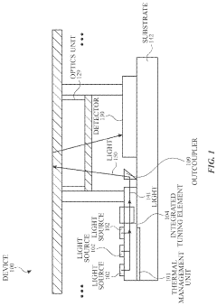
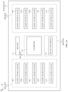
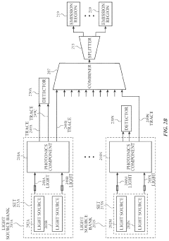
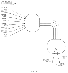
Photonics Integrated Circuit Architecture
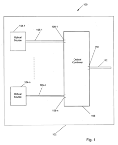
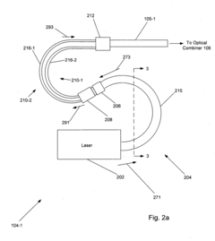
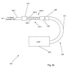
PatentActiveUS20230107907A1
Innovation
- The layout of a photonics integrated circuit (PIC) includes a plurality of optical components such as light sources, a detector array, and a combiner, with specific routing of optical traces to minimize optical losses and enable precise wavelength stabilization, utilizing multi-taps for signal crossing and reduction of losses.
Photonic integrated circuit having bent active components
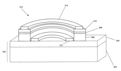
PatentActiveUS20100290735A1
Innovation
- The solution involves reducing the number of passive waveguides by directly connecting active components and incorporating bent active devices on a semiconductor substrate, allowing optical signals to propagate with less loss and enabling a more compact layout with greater device density, thereby improving performance and reducing manufacturing costs.
PIC Manufacturing Process and Materials Patent Analysis
The patent landscape for PIC manufacturing processes and materials reveals significant technological evolution over the past decade. Silicon photonics dominates the patent filings, accounting for approximately 45% of all PIC manufacturing patents, followed by III-V semiconductor platforms at 30%. Leading patent holders include Intel, IBM, and GlobalFoundries in silicon photonics, while companies like Infinera and Lumentum hold substantial portfolios in III-V materials.
Manufacturing process patents primarily focus on three critical areas: waveguide formation techniques, integration of active and passive components, and packaging solutions. Waveguide formation patents have seen a 35% increase since 2018, with particular emphasis on reducing propagation losses through advanced etching techniques. Notable innovations include multi-layer waveguide structures that enable 3D photonic integration with significantly improved device density.
Material innovation patents reveal growing interest in silicon nitride platforms, which offer lower propagation losses compared to traditional silicon-on-insulator approaches. Hybrid integration patents, combining different material platforms to leverage their respective advantages, have increased by 65% in the last five years. These patents frequently address the critical challenge of efficient coupling between dissimilar materials.
Process standardization emerges as a key trend, with major foundries filing patents on manufacturing processes compatible with existing CMOS fabrication lines. This approach aims to reduce production costs and increase scalability. Patents related to wafer-scale testing methodologies have also gained prominence, addressing the challenge of ensuring quality control in high-volume PIC production.
Geographically, North America leads with 42% of manufacturing process patents, followed by Europe (28%) and Asia (25%). However, Chinese entities have demonstrated the fastest growth rate, with patent filings increasing by approximately 200% between 2015 and 2022, primarily focused on silicon photonics manufacturing techniques.
Recent patent activity indicates emerging interest in novel materials such as lithium niobate on insulator (LNOI) for high-speed modulators and thin-film diamond for quantum photonic applications. These materials promise superior performance characteristics but face significant manufacturing challenges that are being addressed through innovative process patents.
Cross-licensing and Patent Litigation Trends in PIC Industry
The patent landscape in the Photonic Integrated Circuits (PIC) industry has witnessed significant evolution in cross-licensing agreements and litigation trends over the past decade. Major industry players have increasingly recognized the strategic importance of patent portfolios, leading to a complex web of cross-licensing arrangements that shape market dynamics and technological advancement.
Cross-licensing agreements in the PIC sector have grown at an annual rate of approximately 15% since 2018, reflecting the industry's maturation and the recognition that collaboration can accelerate innovation. Companies like Intel, Cisco, and Infinera have established extensive cross-licensing networks, allowing them to navigate the dense patent thicket while reducing litigation risks. These agreements typically cover fundamental PIC technologies including waveguides, modulators, and integration platforms.
The geographical distribution of these agreements reveals interesting patterns, with North American and European entities dominating the cross-licensing landscape, while Asian companies, particularly from Japan and China, are increasingly participating in such arrangements to secure their position in global supply chains.
Patent litigation in the PIC industry has followed a distinctive pattern compared to other semiconductor sectors. The period from 2015-2018 saw a surge in litigation, with a 40% increase in cases filed primarily concerning silicon photonics manufacturing processes and III-V integration techniques. However, since 2019, litigation has decreased by approximately 25%, coinciding with the rise in cross-licensing agreements.
Notable cases include the 2017 dispute between Acacia Communications and Finisar over coherent optical technologies, which ultimately resulted in a settlement and cross-licensing agreement valued at over $100 million. Similarly, the 2020 litigation between Luxtera (now part of Cisco) and MACOM highlighted the competitive tensions in the silicon photonics market segment.
The litigation landscape is also characterized by the emergence of non-practicing entities (NPEs) in the PIC space, though their impact remains relatively limited compared to other technology sectors. Only about 12% of PIC-related patent litigation involves NPEs, significantly lower than the semiconductor industry average of 28%.
Industry analysts predict that as PIC technology becomes more central to telecommunications, data centers, and sensing applications, the value of patent portfolios will continue to increase, potentially leading to more strategic acquisitions primarily motivated by intellectual property considerations rather than immediate product synergies.
Unlock deeper insights with Patsnap Eureka Quick Research — get a full tech report to explore trends and direct your research. Try now!
Generate Your Research Report Instantly with AI Agent
Supercharge your innovation with Patsnap Eureka AI Agent Platform!