

How Do Photonic Integrated Circuits Support Enhanced Imaging Systems
SEP 29, 20259 MIN READ
Generate Your Research Report Instantly with AI Agent
Patsnap Eureka helps you evaluate technical feasibility & market potential.
PIC Imaging Technology Background and Objectives
Photonic Integrated Circuits (PICs) represent a revolutionary advancement in the field of optics and photonics, evolving from discrete optical components to highly integrated systems on a single chip. This evolution mirrors the trajectory of electronic integrated circuits but in the domain of light manipulation. The development of PICs dates back to the 1980s, with significant acceleration in the past two decades due to advancements in fabrication technologies and material sciences.
The integration of multiple photonic functions on a single chip has enabled unprecedented capabilities in light processing, sensing, and communication. In the context of imaging systems, PICs offer transformative potential by miniaturizing complex optical systems while enhancing performance parameters such as resolution, sensitivity, and processing speed. The technology evolution trend clearly points toward greater integration density, reduced power consumption, and expanded functionality.
Current imaging technologies face limitations in size, weight, power consumption, and cost (SWaP-C) that PICs can potentially address. Traditional imaging systems rely on bulky optical components and separate electronic processing units, creating barriers to deployment in space-constrained applications such as medical endoscopes, autonomous vehicles, and wearable devices. PICs offer a path to overcome these constraints through monolithic integration of optical and electronic functions.
The primary technical objectives for PIC-based imaging systems include achieving higher resolution beyond conventional diffraction limits, enabling real-time 3D imaging capabilities, reducing form factors by orders of magnitude, and integrating advanced processing capabilities directly within the imaging system. Additionally, there are goals to develop reconfigurable imaging systems that can adapt to different environmental conditions and application requirements on demand.
From a materials perspective, the field is witnessing diversification beyond traditional silicon photonics to include III-V compounds, lithium niobate, and other novel materials that offer enhanced optical properties. This materials evolution is critical for expanding the wavelength ranges and improving the efficiency of PIC-based imaging systems, particularly for applications requiring operation in the infrared or ultraviolet spectra.
The convergence of PICs with complementary technologies such as artificial intelligence, quantum computing, and advanced manufacturing techniques is expected to further accelerate innovation in imaging systems. These technological synergies create opportunities for entirely new imaging modalities that were previously impossible with conventional approaches, such as computational imaging, quantum imaging, and neuromorphic optical processing.
Market Analysis for PIC-Enhanced Imaging Systems
The global market for Photonic Integrated Circuit (PIC) enhanced imaging systems is experiencing robust growth, driven by increasing demand across multiple sectors including healthcare, industrial automation, consumer electronics, and defense. Current market valuations indicate that the PIC-based imaging systems market reached approximately 2.3 billion USD in 2022, with projections suggesting a compound annual growth rate of 23.7% through 2028.
Healthcare represents the largest application segment, accounting for nearly 35% of the total market share. Within this sector, PIC-enhanced imaging technologies are revolutionizing diagnostic capabilities through advanced endoscopy, optical coherence tomography (OCT), and photoacoustic imaging systems. The aging global population and increasing prevalence of chronic diseases are significant market drivers, creating sustained demand for more precise diagnostic tools.
Industrial applications constitute the fastest-growing segment, with machine vision systems for quality control and inspection processes showing particular promise. The integration of PICs into industrial imaging systems has enabled higher resolution, faster processing speeds, and reduced form factors, making them increasingly attractive for manufacturing environments where space constraints and processing requirements are critical considerations.
Consumer electronics applications, particularly in smartphone cameras, augmented reality devices, and autonomous vehicle sensing systems, represent an emerging market with substantial growth potential. The miniaturization capabilities of PICs allow for integration of advanced imaging functionalities in compact consumer devices, driving adoption across this sector.
Regional analysis reveals North America currently leads the market with approximately 40% share, followed by Europe and Asia-Pacific. However, the Asia-Pacific region is expected to witness the highest growth rate over the forecast period, primarily due to increasing industrial automation investments in China, Japan, and South Korea, coupled with the presence of major semiconductor and electronics manufacturing facilities.
Key market restraints include high initial development costs, complex manufacturing processes, and integration challenges with existing systems. The specialized expertise required for PIC design and fabrication also presents a barrier to market entry for smaller companies.
Customer demand trends indicate growing preference for multifunctional imaging systems that combine different sensing modalities (spectral, thermal, 3D) in single integrated platforms. Additionally, there is increasing interest in real-time processing capabilities and AI-enhanced image analysis, suggesting future market opportunities at the intersection of photonics and artificial intelligence technologies.
Current PIC Imaging Technology Landscape and Challenges
Photonic Integrated Circuits (PICs) have emerged as a transformative technology in imaging systems, offering unprecedented capabilities in terms of speed, resolution, and functionality. The current landscape of PIC-based imaging technology is characterized by rapid innovation across multiple domains, from medical diagnostics to autonomous vehicles and industrial inspection systems.
In the medical imaging sector, PICs are enabling new modalities of optical coherence tomography (OCT) and photoacoustic imaging with significantly enhanced resolution. Companies like Luxtera and Ayar Labs have developed PIC platforms that integrate multiple optical components on a single chip, reducing system size by up to 90% while improving imaging depth and contrast. However, these systems still face challenges in achieving the bandwidth necessary for real-time 3D imaging at microscopic scales.
The telecommunications industry has been instrumental in driving PIC development, with companies like Intel and Cisco implementing silicon photonics for high-speed data transmission. These advances are now being repurposed for imaging applications, particularly in LIDAR systems for autonomous vehicles. Current PIC-based LIDAR solutions offer improved range and resolution compared to traditional systems, but struggle with performance degradation in adverse weather conditions.
A significant technical challenge in the current PIC imaging landscape is the integration of different material platforms. While silicon photonics dominates due to compatibility with CMOS fabrication processes, materials like indium phosphide and silicon nitride offer superior performance for specific imaging applications. The industry is actively working on heterogeneous integration techniques, but yield issues and thermal management remain problematic.
Another critical limitation is the coupling efficiency between PICs and external optical components. Current edge-coupling and grating-coupling solutions typically introduce losses of 3-6 dB per connection, significantly reducing overall system performance. Research groups at MIT and Stanford have demonstrated promising approaches using metamaterial-based couplers, but these have yet to be commercialized at scale.
The manufacturing ecosystem for PIC-based imaging systems remains fragmented, with specialized foundries like AIM Photonics and LioniX International offering process development kits that are not fully standardized. This lack of standardization increases development costs and time-to-market for new imaging applications.
Power consumption represents another significant challenge, particularly for portable imaging devices. While PICs offer inherent advantages over electronic circuits in terms of heat generation, the control electronics and thermoelectric coolers required for stable operation can consume several watts of power, limiting battery life in mobile applications.
Despite these challenges, the PIC imaging technology landscape is evolving rapidly, with annual investment exceeding $500 million globally. Emerging solutions like quantum dot integration and on-chip frequency combs promise to address many current limitations, potentially enabling a new generation of compact, high-performance imaging systems across multiple industries.
Current PIC Solutions for Advanced Imaging Applications
01 Integration of photonic circuits with imaging sensors
Photonic integrated circuits can be directly integrated with imaging sensors to enhance imaging capabilities. This integration allows for on-chip processing of optical signals, improving resolution, sensitivity, and speed of image acquisition. The combination enables advanced functionalities such as real-time image processing, spectral filtering, and improved signal-to-noise ratio in imaging applications.- Integration of photonic circuits with imaging sensors: Photonic integrated circuits can be directly integrated with imaging sensors to enhance imaging capabilities. This integration allows for on-chip processing of optical signals, improving resolution, sensitivity, and speed of image acquisition. The combination enables advanced functionalities such as real-time image processing, spectral filtering, and improved signal-to-noise ratio in imaging applications.
- Waveguide-based optical signal routing for imaging: Photonic integrated circuits utilize waveguides to efficiently route optical signals for imaging applications. These waveguides can direct light with minimal loss, enabling complex optical paths within a compact footprint. The technology allows for precise control of light propagation, beam steering, and signal distribution across imaging arrays, resulting in enhanced image quality and system performance.
- On-chip spectral filtering and wavelength management: Photonic integrated circuits can perform spectral filtering and wavelength management directly on-chip, enhancing imaging capabilities across different spectral bands. This technology enables hyperspectral and multispectral imaging by selectively processing specific wavelengths of light. The integration of wavelength-selective components allows for improved contrast, reduced crosstalk, and enhanced feature detection in imaging applications.
- Integrated optical phased arrays for imaging: Photonic integrated circuits can implement optical phased arrays that enable advanced beam steering and focusing capabilities for imaging systems. These arrays provide electronic control of optical beam direction without mechanical components, allowing for rapid scanning and adaptive focusing. The technology enables applications such as LIDAR, 3D imaging, and high-resolution scanning systems with improved speed and reliability.
- Quantum photonic integrated circuits for enhanced imaging: Quantum photonic integrated circuits leverage quantum optical effects to achieve imaging capabilities beyond classical limits. These circuits can generate and manipulate quantum states of light, enabling super-resolution imaging, quantum-enhanced sensing, and ghost imaging techniques. The integration of quantum photonic elements on-chip allows for more compact, stable, and scalable quantum imaging systems with unprecedented sensitivity and resolution.
02 Waveguide-based optical signal processing for imaging
Waveguide structures within photonic integrated circuits can be used to manipulate and process optical signals for enhanced imaging. These waveguides can direct light, perform filtering, splitting, and combining operations that are essential for advanced imaging techniques. The waveguide-based approach allows for compact, efficient optical signal routing and processing that improves image quality and enables novel imaging modalities.Expand Specific Solutions03 Spectral imaging and sensing enhancements
Photonic integrated circuits can enable advanced spectral imaging capabilities by incorporating wavelength-selective components. These circuits can perform on-chip spectral analysis, multi-spectral imaging, and hyperspectral sensing with high precision. The integration of spectral filtering and detection elements on a single chip allows for more compact and efficient spectral imaging systems with applications in medical diagnostics, environmental monitoring, and industrial inspection.Expand Specific Solutions04 Quantum photonic integrated circuits for imaging
Quantum photonic integrated circuits leverage quantum optical effects to achieve imaging capabilities beyond classical limits. These circuits can generate, manipulate, and detect quantum states of light for applications such as quantum-enhanced imaging, ghost imaging, and quantum sensing. The quantum approach enables super-resolution imaging, improved sensitivity in low-light conditions, and novel imaging modalities that exploit quantum correlations.Expand Specific Solutions05 3D and holographic imaging using photonic integrated circuits
Photonic integrated circuits can be designed to enable advanced 3D and holographic imaging capabilities. These circuits incorporate phase manipulation components, beam steering elements, and specialized optical processing units to capture or generate three-dimensional visual information. The integration of these functions on a single photonic chip allows for compact, efficient systems for applications in augmented reality, volumetric displays, and 3D machine vision.Expand Specific Solutions
Key Industry Players in Photonic Integrated Circuits
Photonic Integrated Circuits (PICs) for enhanced imaging systems are currently in a growth phase, with the market expected to reach significant expansion as applications diversify across medical imaging, autonomous vehicles, and surveillance. The technology maturity varies across players, with established semiconductor giants like Taiwan Semiconductor Manufacturing Co. and Intel Corp. leveraging their manufacturing expertise to develop advanced PIC platforms. Research institutions including MIT, California Institute of Technology, and Peking University are driving fundamental innovations, while specialized companies such as Lightmatter, SMART Photonics, and Lumentum Operations are commercializing cutting-edge solutions. The competitive landscape features collaboration between academic institutions and industry players, with companies like Northrop Grumman and Samsung Electro-Mechanics integrating PICs into sophisticated imaging systems for defense and consumer applications.
Taiwan Semiconductor Manufacturing Co., Ltd.
Technical Solution: TSMC has developed an advanced silicon photonics platform that integrates optical components with CMOS electronics for enhanced imaging applications. Their technology enables the fabrication of high-density photonic integrated circuits featuring waveguides with propagation losses below 0.2 dB/cm and efficient grating couplers with insertion losses under 1.5 dB. TSMC's photonic integration approach incorporates germanium photodetectors with responsivity exceeding 1 A/W across the near-infrared spectrum, critical for high-sensitivity imaging. The company has demonstrated monolithic integration of photonic components with advanced CMOS nodes (7nm and below), enabling sophisticated on-chip image processing capabilities. Their silicon photonics platform supports multi-project wafer runs, accelerating the development cycle for novel imaging PIC designs. TSMC has pioneered wafer-scale testing methodologies for photonic circuits, ensuring high yield and reliability for imaging applications.
Strengths: World-leading semiconductor manufacturing infrastructure; ability to integrate photonics with advanced CMOS nodes; exceptional process control and yield management. Weaknesses: Limited in-house design expertise for imaging-specific applications; reliance on external IP for specialized optical functions.
Intel Corp.
Technical Solution: Intel has developed silicon photonics technology that integrates lasers, modulators, and detectors on silicon substrates for enhanced imaging applications. Their RealSense technology incorporates photonic integrated circuits (PICs) to enable depth sensing and 3D imaging capabilities. Intel's silicon photonics platform utilizes hybrid integration of III-V materials with silicon waveguides to achieve high-performance optical interconnects and sensing capabilities. The company has demonstrated PICs with integrated germanium photodetectors achieving >30GHz bandwidth and low dark current, essential for high-resolution imaging systems. Intel's photonic integration approach enables wavelength division multiplexing (WDM) for multi-spectral imaging applications, allowing simultaneous capture of different spectral bands on a single chip.
Strengths: Mature silicon fabrication infrastructure allows for high-volume, low-cost production of PICs; strong expertise in heterogeneous integration of III-V materials with silicon. Weaknesses: Relatively higher optical losses compared to specialized photonic materials; challenges in integrating efficient light sources directly on silicon.
Core Innovations in PIC-Based Imaging Technologies
Photonic integrated circuit-based imaging systems
PatentActiveUS11815714B2
Innovation
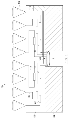
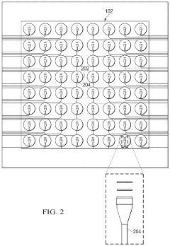
- The implementation of a photonic integrated circuit-based imaging system with a first and second pupil of different sizes, utilizing a waveguide layer with multiple waveguides to guide optical signals between antenna element arrays, and incorporating path length matching and wavelength selection devices to compensate for fabrication tolerances and control wavelengths.
Hybrid integration for photonic integrated circuits
PatentActiveUS11340400B2
Innovation
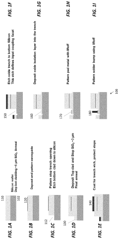
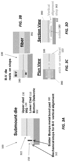
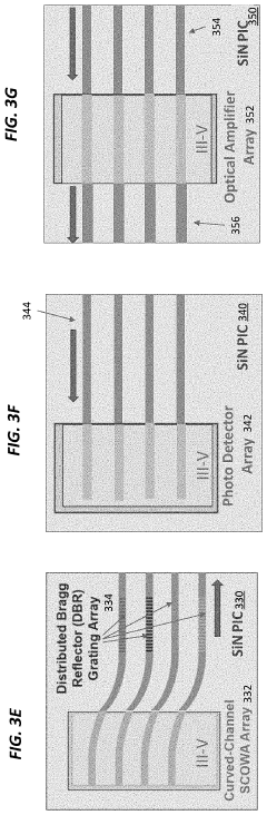
- Hybrid integration techniques that allow coupling of light between silicon PICs and photonic devices from III-V or II-VI materials using silicon oxide claddings, trenches, and pedestals for precise alignment and electrical connection, enabling the integration of light sources, lasers, and optical amplifiers.
Manufacturing Processes and Materials for PICs
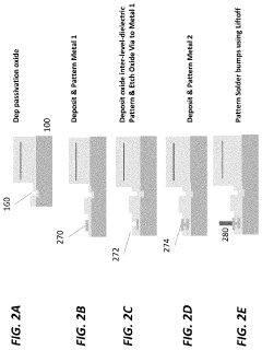
The manufacturing of Photonic Integrated Circuits (PICs) involves sophisticated processes that directly impact their performance in imaging applications. Silicon photonics remains the dominant material platform, leveraging established CMOS fabrication infrastructure while offering excellent optical properties. The manufacturing process typically begins with wafer preparation, followed by lithography to define nanoscale features critical for waveguides and other photonic components. Advanced lithography techniques such as deep-UV and electron-beam lithography enable feature sizes below 100nm, essential for high-density integration in imaging systems.
Etching processes, particularly reactive ion etching, create the three-dimensional structures necessary for light manipulation. The precision of these etching steps directly influences waveguide quality and consequently affects the resolution capabilities of PIC-based imaging systems. Deposition techniques including chemical vapor deposition and atomic layer deposition are employed to create multi-layer structures with precisely controlled thicknesses, critical for wavelength-specific imaging applications.
Material selection represents another crucial aspect of PIC manufacturing for imaging systems. While silicon-on-insulator (SOI) platforms dominate due to their compatibility with existing semiconductor infrastructure, alternative materials offer specialized advantages. Indium phosphide (InP) enables direct integration of light sources and detectors, beneficial for compact imaging systems. Silicon nitride provides superior performance in visible wavelength applications, expanding the spectral range of PIC-based imaging. Lithium niobate offers exceptional electro-optic properties for high-speed modulation in dynamic imaging scenarios.
Recent manufacturing innovations include heterogeneous integration techniques that combine different material platforms to leverage their respective advantages. For example, III-V materials can be bonded to silicon substrates to incorporate efficient light sources directly into silicon photonic circuits, enabling fully integrated imaging solutions. This approach addresses one of the fundamental challenges in silicon photonics—the indirect bandgap limitation that hinders efficient light emission.
Packaging represents the final critical manufacturing step, with particular importance for imaging applications where optical alignment precision directly impacts system performance. Techniques such as flip-chip bonding and optical interposers enable reliable connections between PICs and external components. Advanced packaging approaches incorporating micro-optical elements facilitate efficient light coupling between the PIC and the imaging environment, maximizing system sensitivity and resolution.
Manufacturing yield and reliability remain ongoing challenges, particularly as PIC complexity increases to support sophisticated imaging functionalities. Process control innovations, including in-line optical testing and automated defect detection, are being developed to address these challenges and reduce production costs, ultimately accelerating the adoption of PIC technology in next-generation imaging systems.
Standardization Efforts in Photonic Integration
The standardization of photonic integrated circuits (PICs) represents a critical foundation for their widespread adoption in advanced imaging systems. Currently, several international bodies are actively developing standards to ensure interoperability, reliability, and scalability across the photonic integration ecosystem. The IEEE P3172 working group has established frameworks for optical interface specifications, focusing on standardizing waveguide dimensions, coupling methodologies, and optical I/O parameters specifically relevant to imaging applications.
The Photonic Integrated Circuit Manufacturing Technology Consortium (PIC-MTC) has made significant progress in standardizing fabrication processes, material specifications, and testing protocols. Their recent publication of the "PIC Design Rule Manual 2.0" provides comprehensive guidelines for designing PICs compatible with multi-project wafer (MPW) runs, enabling cost-effective prototyping for imaging system developers.
In Europe, the European Telecommunications Standards Institute (ETSI) has formed a specialized group addressing photonic integration standards with particular attention to imaging applications. Their ISG-PDL (Industry Specification Group on Photonic Design Libraries) has released specifications for standardized building blocks that facilitate the design of imaging-specific photonic circuits, including waveguide-based beam steering components and on-chip spectrometers.
The American National Standards Institute (ANSI) and the International Electrotechnical Commission (IEC) have jointly developed the IEC 63068 series, which standardizes optical performance metrics and testing methodologies for PICs in imaging systems. These standards establish uniform methods for characterizing parameters such as insertion loss, crosstalk, and wavelength accuracy—all critical for imaging applications requiring precise light manipulation.
Open-source initiatives like EPDA (Electronic Photonic Design Automation) Alliance are complementing formal standardization efforts by developing standardized Process Design Kits (PDKs) and design methodologies. Their recent release of the OpenPIC framework provides standardized component libraries specifically optimized for imaging applications, including standardized interfaces for sensor integration and signal processing.
The Optical Internetworking Forum (OIF) has expanded its scope to include standards for high-speed optical interconnects within PIC-based imaging systems, addressing the growing need for efficient data transfer between photonic sensors and electronic processing units. Their Implementation Agreement IA.PIC-IMG-01 specifically addresses the standardization of optical interfaces between imaging PICs and electronic control systems.
Unlock deeper insights with Patsnap Eureka Quick Research — get a full tech report to explore trends and direct your research. Try now!
Generate Your Research Report Instantly with AI Agent
Supercharge your innovation with Patsnap Eureka AI Agent Platform!