What Factors Influence the Efficiency of Photonic Integrated Circuits
SEP 29, 20259 MIN READ
Generate Your Research Report Instantly with AI Agent
Patsnap Eureka helps you evaluate technical feasibility & market potential.
PIC Technology Evolution and Efficiency Goals
Photonic Integrated Circuits (PICs) represent a revolutionary advancement in optical communication technology, evolving from discrete optical components to highly integrated systems on a single chip. The journey began in the 1980s with rudimentary integration of waveguides and simple optical functions, progressing through several distinct evolutionary phases. By the early 2000s, the technology had matured to incorporate multiple optical functions on silicon substrates, marking the beginning of silicon photonics as a dominant approach.
The evolution of PIC technology has been driven by increasing demands for data transmission capacity, energy efficiency, and miniaturization in telecommunications and data centers. Each generation has achieved significant improvements in integration density, from early circuits with just a few components to modern PICs containing thousands of optical elements on a single chip. This progression mirrors the development trajectory seen in electronic integrated circuits, albeit at a different pace and scale.
Current efficiency goals for PICs center around several critical parameters. Power efficiency stands as a primary objective, with researchers aiming to reduce optical losses and improve the conversion efficiency between electrical and optical domains. Integration density represents another crucial target, with ongoing efforts to pack more optical functions into smaller footprints while maintaining performance integrity. Additionally, thermal management has emerged as a significant challenge, as heat generation can severely impact the operational stability and reliability of photonic circuits.
Manufacturing scalability constitutes a parallel efficiency goal, focusing on developing fabrication processes compatible with existing semiconductor manufacturing infrastructure to enable cost-effective mass production. The industry is actively pursuing standardization of design methodologies and process technologies to facilitate broader adoption and commercialization of PIC solutions across various application domains.
Recent technological breakthroughs have expanded the potential applications of PICs beyond traditional telecommunications into emerging fields such as quantum computing, biosensing, and autonomous vehicle navigation. These new application areas introduce additional efficiency requirements, including enhanced sensitivity for sensing applications, ultra-low latency for real-time processing, and quantum coherence preservation for quantum information processing.
The efficiency goals for PICs are increasingly being shaped by sustainability considerations as well. As data centers and communication networks consume growing portions of global energy resources, developing PICs with minimal energy footprints has become a strategic priority. Research initiatives are exploring novel materials and architectures that could dramatically reduce the energy consumption of optical signal processing and transmission, potentially enabling order-of-magnitude improvements in overall system efficiency.
Market Demand Analysis for High-Efficiency PICs
The global market for high-efficiency Photonic Integrated Circuits (PICs) is experiencing robust growth, driven primarily by the increasing demand for high-speed data transmission and processing capabilities. Current market analyses indicate that the PIC market is expanding at a compound annual growth rate exceeding 20%, with particular acceleration in telecommunications, data centers, and emerging quantum computing applications.
Telecommunications remains the dominant application sector, where the need for higher bandwidth and energy efficiency is pushing operators toward PIC-based solutions. The transition to 5G and future 6G networks has created substantial demand for PICs capable of handling massive data throughput while maintaining signal integrity across longer distances. Network providers are specifically seeking PICs with reduced insertion loss and enhanced wavelength division multiplexing capabilities.
Data center operators represent another significant market segment, facing unprecedented challenges in managing energy consumption while scaling computing power. High-efficiency PICs offer a compelling solution by enabling optical interconnects that consume substantially less power than traditional electronic interconnects. Market research indicates that data centers implementing PIC-based interconnects can achieve energy savings of up to 30% in their networking infrastructure, creating a strong economic incentive for adoption.
The emerging field of quantum computing presents a specialized but rapidly growing market for advanced PICs. Quantum information processing requires precise photon manipulation capabilities that only sophisticated integrated photonic platforms can provide. As quantum computing moves from research laboratories toward commercial applications, demand for specialized high-efficiency PICs is projected to grow exponentially.
Consumer electronics manufacturers are increasingly exploring PIC integration for next-generation devices. Applications include advanced sensing capabilities for smartphones, augmented reality displays, and autonomous vehicle LiDAR systems. This market segment values miniaturization and power efficiency, creating demand for PICs with higher integration density and lower power consumption.
Healthcare applications represent another expanding market, with optical biosensors based on PIC technology enabling rapid, sensitive diagnostics. The market for PIC-based medical devices is growing as healthcare providers seek point-of-care testing solutions with laboratory-grade accuracy. This sector particularly values PICs with enhanced sensitivity and specificity for biomolecule detection.
Market barriers include the relatively high cost of PIC manufacturing and packaging, which currently limits mass-market adoption. However, industry analysts predict that continued advances in manufacturing processes will drive costs down significantly over the next five years, opening new market segments. The development of standardized design and manufacturing platforms is expected to further accelerate market growth by reducing development cycles and entry barriers for new applications.
Current Efficiency Limitations and Challenges
Despite significant advancements in photonic integrated circuit (PIC) technology, several critical efficiency limitations and challenges persist that hinder optimal performance. Propagation losses remain one of the most fundamental challenges, with material absorption, sidewall roughness, and radiation losses collectively diminishing signal integrity across the circuit. Silicon-based PICs typically experience losses of 0.1-3 dB/cm, while polymer waveguides may suffer 0.5-5 dB/cm losses depending on fabrication quality and operating wavelength.
Coupling efficiency between different components presents another significant barrier, particularly at interfaces between optical fibers and on-chip waveguides where mode mismatch can result in coupling losses exceeding 3 dB per facet without specialized coupling structures. Even with advanced edge or grating couplers, coupling losses rarely drop below 0.5 dB, creating substantial performance penalties in complex circuits.
Thermal management has emerged as a critical challenge as integration density increases. Temperature fluctuations affect refractive indices and resonant wavelengths, causing performance drift in temperature-sensitive components like ring resonators and Mach-Zehnder interferometers. Current thermal stabilization techniques consume significant power, with thermal tuning often requiring 10-50 mW per active component, limiting the scalability of large-scale PICs.
Manufacturing variability introduces dimensional deviations that significantly impact device performance. Even state-of-the-art fabrication processes exhibit variations of ±5-10 nm in critical dimensions, resulting in wavelength shifts of several nanometers in resonant structures and phase errors in interferometric devices. These variations necessitate post-fabrication trimming or active tuning, increasing complexity and power consumption.
Polarization management remains challenging in most PIC platforms, with many waveguide geometries supporting both TE and TM modes with different propagation characteristics. Polarization-dependent loss and birefringence can cause signal degradation in polarization-sensitive applications, while polarization mode dispersion limits bandwidth in high-speed communications systems.
Integration of active components, particularly efficient light sources, presents a fundamental challenge for silicon photonics due to silicon's indirect bandgap. While hybrid integration approaches using III-V materials have shown promise, they introduce additional coupling interfaces and alignment challenges, with typical laser-to-waveguide coupling efficiencies ranging from 30-70% depending on integration method.
Nonlinear effects become increasingly problematic at higher optical powers, with two-photon absorption in silicon limiting power handling to approximately 5-10 mW in typical waveguides before efficiency degradation occurs. These power limitations constrain the signal-to-noise ratio achievable in many applications and restrict the scaling of certain nonlinear optical processes.
Current Efficiency Enhancement Solutions
01 Novel materials and structures for improved PIC efficiency
Advanced materials and innovative structural designs can significantly enhance the efficiency of photonic integrated circuits. These include the use of novel semiconductor materials, metamaterials, and optimized waveguide structures that reduce propagation losses and improve light confinement. Multi-layer structures and specialized substrates can also contribute to better thermal management and reduced optical losses, resulting in higher overall circuit efficiency.- Integration of optical components for improved efficiency: Photonic integrated circuits (PICs) can achieve higher efficiency through the integration of multiple optical components on a single chip. This approach reduces coupling losses between components and minimizes the overall footprint. Advanced integration techniques allow for the combination of lasers, modulators, waveguides, and detectors in compact configurations, leading to improved signal transmission and reduced power consumption. These integrated designs enable more efficient light manipulation and processing for various applications.
- Novel waveguide structures for enhanced light propagation: Specialized waveguide structures can significantly improve the efficiency of photonic integrated circuits. These include silicon-based waveguides, slot waveguides, and photonic crystal waveguides that offer better confinement of light and reduced propagation losses. By optimizing the geometry, material composition, and fabrication processes of these waveguides, engineers can achieve higher transmission efficiency and better control over optical modes. These advanced waveguide designs enable more efficient routing of optical signals across the photonic chip.
- Coupling techniques for reduced insertion loss: Efficient coupling between external light sources and photonic integrated circuits is crucial for overall system performance. Various coupling techniques, including grating couplers, edge couplers, and tapered waveguides, have been developed to minimize insertion losses at the interfaces. These approaches optimize the mode matching between different optical components and ensure efficient light transfer. Advanced coupling methods can significantly reduce the power loss at critical junctions, thereby enhancing the overall efficiency of photonic integrated circuits.
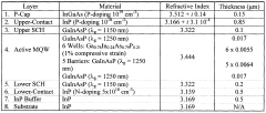
- Materials engineering for improved optical performance: The selection and engineering of materials play a vital role in enhancing the efficiency of photonic integrated circuits. Novel materials such as silicon nitride, indium phosphide, lithium niobate, and various III-V compounds offer unique optical properties that can be leveraged for specific applications. By carefully designing material compositions, creating heterostructures, or incorporating quantum wells, the performance of active and passive components can be significantly improved. These material innovations lead to reduced optical losses, enhanced nonlinear effects, and better thermal management.
- Advanced fabrication and packaging techniques: State-of-the-art fabrication and packaging methods contribute significantly to the efficiency of photonic integrated circuits. Techniques such as wafer-scale integration, 3D stacking, and hybrid integration enable more complex and efficient photonic systems. Precision manufacturing processes, including advanced lithography, etching, and deposition techniques, help minimize fabrication imperfections that can cause scattering losses. Additionally, innovative packaging solutions that address thermal management, fiber alignment, and environmental protection ensure that the theoretical efficiency of PICs is maintained in practical applications.
02 Integration techniques for optical and electronic components
Efficient integration of optical and electronic components on a single chip is crucial for PIC performance. Various techniques such as monolithic integration, heterogeneous integration, and hybrid bonding methods enable the combination of different functional elements while minimizing coupling losses. These approaches allow for compact designs with optimized interfaces between photonic and electronic domains, resulting in improved signal integrity and reduced power consumption.Expand Specific Solutions03 Coupling and waveguide optimization for enhanced efficiency
Efficient light coupling between components and optimized waveguide designs are essential for minimizing losses in photonic integrated circuits. Advanced coupling structures, including grating couplers, tapered waveguides, and mode converters, can significantly improve the transfer of optical signals between different parts of the circuit. Waveguide geometry optimization, including cross-sectional design and bend radius considerations, further reduces propagation losses and improves overall circuit efficiency.Expand Specific Solutions04 Active components and modulation techniques
Efficient active components and modulation techniques are critical for high-performance PICs. These include advanced laser sources, high-speed modulators, and photodetectors with improved quantum efficiency. Novel modulation schemes, such as electro-optic and thermo-optic modulation, can achieve higher data rates with lower power consumption. Integration of efficient amplifiers and the use of resonant structures further enhance the performance of active photonic components.Expand Specific Solutions05 Thermal management and packaging solutions
Effective thermal management and advanced packaging solutions are essential for maintaining the efficiency of photonic integrated circuits. Heat dissipation techniques, including integrated heat sinks, thermal vias, and specialized substrate materials, help prevent performance degradation due to temperature variations. Novel packaging approaches that provide hermetic sealing, precise alignment of optical components, and efficient electrical connections contribute to improved reliability and long-term stability of PICs.Expand Specific Solutions
Key Industry Players and Competitive Landscape
The photonic integrated circuits (PICs) market is currently in a growth phase, with an estimated market size of $1.5 billion and projected to reach $5.2 billion by 2027. The technology maturity varies across applications, with telecommunications being most advanced while quantum computing applications remain nascent. Leading semiconductor giants like TSMC and Intel are investing heavily in silicon photonics manufacturing capabilities, while specialized players such as PsiQuantum, Lightmatter, and SMART Photonics are driving innovation in quantum computing and AI applications. Academic-industry partnerships involving institutions like Shanghai Jiao Tong University and IMEC are accelerating technology transfer. The competitive landscape is characterized by a mix of established semiconductor manufacturers expanding their portfolios and specialized photonics startups focusing on niche applications, with increasing consolidation expected as the technology matures.
Taiwan Semiconductor Manufacturing Co., Ltd.
Technical Solution: TSMC has developed advanced silicon photonics integration platforms that address key efficiency factors in PICs. Their 300mm silicon photonics process combines low-loss silicon nitride (SiN) waveguides with silicon waveguides to optimize both propagation losses and integration density. TSMC's platform features specialized germanium photodetectors with high responsivity (>0.8 A/W) and low dark current, critical for efficient optical-to-electrical conversion. The company has implemented advanced lithography techniques to create sub-wavelength gratings and metamaterial structures that enhance light coupling efficiency and reduce polarization dependence. Their process incorporates precision doping profiles for efficient modulators with VπL products below 1V·cm, enabling high-speed operation with reduced power consumption. TSMC's backend integration capabilities allow for 3D stacking of photonic and electronic dies through advanced packaging solutions, minimizing interconnect distances and associated losses while enabling heterogeneous integration of different material platforms.
Strengths: World-class manufacturing capabilities with high yield and volume production; advanced process control ensuring tight tolerances; comprehensive electronic-photonic integration. Weaknesses: Less experience with active photonic components compared to III-V platforms; primarily focused on silicon photonics rather than specialized photonic materials; higher cost for low-volume prototyping.
Intel Corp.
Technical Solution: Intel has developed silicon photonics technology that integrates lasers directly onto silicon chips, addressing key efficiency factors in PICs. Their approach uses hybrid silicon integration where III-V materials are bonded to silicon waveguides, enabling on-chip light generation while leveraging existing CMOS manufacturing infrastructure. Intel's co-packaged optics solutions combine photonic ICs with electronic ICs in the same package, minimizing transmission distances and reducing power consumption. Their 400G and 800G transceivers utilize advanced multiplexing techniques and wavelength division multiplexing to increase bandwidth density. Intel has also pioneered techniques to reduce coupling losses between fiber and chip through edge and grating couplers optimized for high efficiency, achieving coupling losses below 1dB in some configurations.
Strengths: Mature CMOS manufacturing capabilities allow for high-volume production; strong integration with electronic components; advanced packaging solutions. Weaknesses: Relatively higher propagation losses compared to specialized photonic materials; thermal management challenges in densely integrated designs; limited in-house III-V material expertise compared to pure-play photonics companies.
Critical Materials and Fabrication Innovations
Enhanced efficiency laterally-coupled distributed feedback laser
PatentWO2009055894A1
Innovation
- The design of a laterally-coupled DFB laser with a surface etched grating, specifically optimized to operate in the first order mode, using a single-step epitaxial growth process, which enhances coupling and quantum efficiency by suppressing the zero order mode through gain-loss discrimination, allowing for monolithic integration with other PIC elements.


Low Temperature Fabrication of Silicon Nitride Photonic Devices
PatentPendingUS20240210625A1
Innovation
- A low-temperature fabrication method using inductively coupled plasma-plasma enhanced chemical vapor deposition (ICP-PECVD) with deuterated silane and nitrogen precursors to deposit silicon nitride or silicon oxynitride waveguide materials, allowing for waveguide fabrication at temperatures below 250°C, compatible with a wide range of substrates and materials.
Thermal Management Strategies in PICs
Thermal management represents a critical challenge in photonic integrated circuits (PICs) development, as temperature fluctuations significantly impact device performance and reliability. The dense integration of optical components generates considerable heat, which must be efficiently dissipated to maintain optimal operation. Current thermal management strategies in PICs can be categorized into passive and active approaches, each with distinct advantages and implementation considerations.
Passive thermal management techniques focus on materials and structural design to enhance heat dissipation without requiring external power. High thermal conductivity substrates such as silicon carbide and diamond-based materials have emerged as promising alternatives to traditional silicon platforms, offering superior heat dissipation properties. Thermal vias and through-silicon vias (TSVs) strategically placed throughout the PIC layout create dedicated thermal pathways that efficiently channel heat away from critical components.
Advanced packaging solutions also play a crucial role in passive thermal management. Flip-chip bonding techniques enable direct contact between heat-generating components and heat sinks, minimizing thermal resistance. Similarly, the integration of thermal underfill materials with enhanced thermal conductivity improves heat transfer across interfaces while providing mechanical stability to the assembly.
Active thermal management approaches incorporate dynamic control mechanisms to regulate temperature distribution across the PIC. Thermoelectric coolers (TECs) based on the Peltier effect provide localized cooling capabilities, enabling precise temperature control for temperature-sensitive components such as lasers and modulators. Microfluidic cooling channels integrated within the PIC substrate offer another active solution, where liquid coolants circulating through microscale channels efficiently extract heat from the device.
Recent innovations in thermal management include the development of phase-change materials (PCMs) that absorb excess heat during operation by undergoing phase transitions. These materials provide thermal buffering capabilities, preventing rapid temperature fluctuations that could degrade performance. Additionally, advanced thermal simulation tools now enable accurate prediction of hotspots and thermal gradients during the design phase, allowing engineers to optimize component placement and thermal management structures before fabrication.
The selection of appropriate thermal management strategies depends on several factors including power density, operating environment, cost constraints, and reliability requirements. For high-power applications such as optical transceivers in data centers, comprehensive solutions combining multiple approaches may be necessary. Conversely, low-power sensing applications might require only minimal thermal management to maintain acceptable performance levels.
Standardization Efforts in PIC Manufacturing
Standardization efforts in the photonic integrated circuit (PIC) manufacturing landscape have emerged as a critical factor influencing overall efficiency and industry growth. The fragmented nature of PIC manufacturing processes has historically created significant barriers to mass production and cost reduction. Unlike the electronic integrated circuit industry, which benefits from decades of standardization, the PIC ecosystem continues to struggle with compatibility issues across different manufacturing platforms.
Several industry consortia have formed to address these challenges, with organizations like the American Institute for Manufacturing Integrated Photonics (AIM Photonics) and the European Photonics Industry Consortium (EPIC) leading standardization initiatives. These efforts focus on establishing common design rules, process design kits (PDKs), and manufacturing protocols that enable seamless integration between different foundries and design houses.
The development of standardized PDKs represents a particularly significant advancement, as these toolkits provide designers with verified component libraries and accurate models that reflect the manufacturing capabilities of specific foundries. This standardization reduces design iterations and improves first-pass success rates, directly enhancing manufacturing efficiency.
Material standardization has also gained momentum, with silicon photonics emerging as a dominant platform due to its compatibility with CMOS manufacturing infrastructure. However, specialized applications often require alternative material systems such as indium phosphide or silicon nitride, necessitating parallel standardization efforts across multiple material platforms.
Testing and characterization protocols present another critical area for standardization. The industry is working toward unified measurement techniques and quality metrics that enable meaningful comparison between different PIC solutions. These standards help identify manufacturing inconsistencies and provide clear benchmarks for performance evaluation.
Packaging and interface standards represent perhaps the most challenging frontier, as they must bridge the gap between photonic and electronic domains. Efforts to standardize optical I/O, fiber coupling techniques, and electronic-photonic co-packaging are essential for improving overall system efficiency and reducing assembly costs.
The economic impact of these standardization initiatives cannot be overstated. Research indicates that comprehensive standardization could reduce PIC development costs by up to 40% while accelerating time-to-market by 30%. Furthermore, standardization facilitates the emergence of a more diverse supply chain, reducing dependency on proprietary technologies and fostering innovation through increased competition and collaboration.
Unlock deeper insights with Patsnap Eureka Quick Research — get a full tech report to explore trends and direct your research. Try now!
Generate Your Research Report Instantly with AI Agent
Supercharge your innovation with Patsnap Eureka AI Agent Platform!