Photonic Integrated Circuits for Next-Generation Wearable Devices
SEP 29, 20259 MIN READ
Generate Your Research Report Instantly with AI Agent
Patsnap Eureka helps you evaluate technical feasibility & market potential.
PIC Technology Evolution and Objectives
Photonic Integrated Circuits (PICs) have evolved significantly over the past decades, transforming from bulky laboratory setups to miniaturized chips capable of manipulating light at microscopic scales. The evolution began in the 1980s with simple waveguide structures and has now advanced to complex systems integrating multiple photonic components on a single substrate. This progression mirrors the development trajectory of electronic integrated circuits but with unique challenges related to light manipulation rather than electron flow.
The fundamental technology behind PICs involves the integration of multiple photonic functions such as light generation, modulation, transmission, and detection on a single chip platform. Early developments focused primarily on telecommunications applications, but recent advancements have expanded potential use cases significantly, particularly in wearable technology where size, power efficiency, and functionality convergence are critical factors.
Current PIC technology employs various material platforms including silicon photonics, indium phosphide, silicon nitride, and polymer-based systems. Each offers distinct advantages: silicon photonics leverages existing CMOS fabrication infrastructure; indium phosphide excels in light emission; silicon nitride provides superior optical properties for passive components; while polymer systems offer flexibility and cost advantages for certain applications.
For next-generation wearable devices, the technological objectives of PIC development are multifaceted. Primary goals include dramatic miniaturization to accommodate the form factor constraints of wearable devices while maintaining or enhancing functionality. Power efficiency represents another critical objective, as wearable devices operate under strict energy budgets. PICs offer inherent advantages in this regard, potentially consuming orders of magnitude less power than electronic equivalents for certain operations.
Integration density improvement constitutes another key objective, aiming to incorporate more photonic functions per unit area. This includes the development of novel multiplexing techniques, 3D integration approaches, and heterogeneous integration of different material platforms to combine their respective advantages. The target is to achieve photonic systems-on-chip that can handle complex sensing, communication, and data processing tasks within the confined spaces of wearable form factors.
Manufacturability at scale represents a significant technological objective, requiring standardization of design processes, improved fabrication yields, and cost-effective packaging solutions. The industry aims to develop PIC platforms that can be mass-produced with consistent performance characteristics, essential for widespread adoption in consumer wearable markets.
The convergence of these technological objectives is driving research toward PICs that can enable unprecedented capabilities in wearable devices, including real-time health monitoring with multiple biomarkers, augmented reality displays with minimal power consumption, and ultra-fast short-range communications for body area networks.
Wearable Market Demand Analysis
The wearable technology market has experienced exponential growth over the past decade, evolving from simple fitness trackers to sophisticated health monitoring systems. Current market analysis indicates that the global wearable market is projected to reach $118.16 billion by 2028, with a compound annual growth rate of 18.5% from 2021 to 2028. This remarkable growth trajectory is primarily driven by increasing health consciousness among consumers, rising chronic disease prevalence, and technological advancements in miniaturization and connectivity.
Consumer demand for wearable devices has shifted significantly toward more sophisticated functionalities beyond basic activity tracking. Modern consumers seek devices that offer comprehensive health monitoring capabilities, including continuous glucose monitoring, blood pressure tracking, ECG measurements, and sleep analysis. This shift represents a substantial market opportunity for photonic integrated circuits (PICs), which can enable these advanced sensing capabilities while maintaining the form factor and power efficiency required for wearable applications.
Healthcare applications represent the fastest-growing segment within the wearable market, with a projected growth rate of 20.1% annually. Medical professionals and healthcare systems increasingly recognize the value of continuous patient monitoring through wearable technology, creating demand for more accurate, reliable, and medically certified devices. PICs offer superior sensing precision compared to traditional electronic circuits, positioning them as ideal components for next-generation medical wearables.
Market research indicates that 67% of consumers consider battery life as a critical factor influencing their wearable device purchasing decisions. The power efficiency advantages of photonic integrated circuits directly address this market need, potentially extending device operation time by 40-60% compared to conventional electronic solutions. This efficiency gain represents a significant competitive advantage in the consumer wearable space.
Regional analysis shows that North America currently holds the largest market share at 36.4%, followed by Europe at 28.7% and Asia-Pacific at 24.3%. However, the Asia-Pacific region is expected to witness the highest growth rate due to increasing disposable income, growing health awareness, and substantial investments in technology infrastructure. This regional growth pattern suggests strategic market entry points for PIC-based wearable technologies.
Industry surveys reveal that 72% of consumers express interest in wearable devices with expanded functionality beyond current offerings, particularly in areas of preventive health monitoring and personalized health insights. This consumer readiness indicates a receptive market for the advanced capabilities that photonic integrated circuits can enable in next-generation wearable devices, including spectroscopic analysis, higher-resolution sensing, and multi-parameter monitoring in compact form factors.
PIC Implementation Challenges
Despite significant advancements in photonic integrated circuits (PICs), their implementation in next-generation wearable devices faces substantial challenges. The miniaturization requirements for wearable applications demand unprecedented levels of integration density, creating significant design constraints. Current PIC platforms struggle to achieve the necessary component density while maintaining optical performance, particularly when transitioning from laboratory demonstrations to mass-producible designs.
Power consumption represents another critical barrier. Wearable devices operate under strict energy budgets, typically powered by small batteries with limited capacity. Traditional optical-electrical-optical (OEO) conversion processes consume substantial power, negating many of the energy advantages that photonics could potentially offer. Developing ultra-low-power photonic components and minimizing conversion stages remains technically challenging.
Thermal management presents unique difficulties in the wearable context. PICs generate heat during operation, and the compact form factor of wearables provides limited options for heat dissipation. This thermal challenge is compounded by the temperature sensitivity of many photonic components, whose performance characteristics can drift significantly with temperature variations, affecting system reliability and precision.
Manufacturing scalability constitutes a fundamental implementation hurdle. While silicon photonics has made progress in leveraging CMOS infrastructure, achieving consistent yields at the scale required for consumer wearables remains problematic. Process variations can significantly impact optical component performance, requiring sophisticated compensation techniques or potentially costly testing procedures.
Integration with existing electronic systems presents additional complexity. Wearable devices require seamless interaction between photonic and electronic components, necessitating sophisticated co-design approaches and potentially novel packaging solutions. The interface between these different technology domains introduces signal integrity challenges and potential reliability concerns.
Cost considerations further complicate PIC implementation in wearables. Consumer wearable devices face intense price pressure, requiring manufacturing processes that can deliver sophisticated photonic functionality at competitive price points. Current fabrication approaches for high-performance PICs often involve expensive materials or complex processing steps incompatible with mass-market economics.
Reliability and environmental robustness represent significant concerns for wearable applications. Unlike datacenter environments, wearable devices must function across varying temperatures, humidity levels, and mechanical stresses. Ensuring consistent optical performance under these dynamic conditions requires advanced packaging solutions and potentially new approaches to component design and materials selection.
Current PIC Solutions for Wearables
01 Integration of optical components on a single chip
Photonic integrated circuits (PICs) involve the integration of multiple optical components such as waveguides, modulators, detectors, and light sources on a single chip. This integration enables compact, high-performance optical systems with reduced size, weight, and power consumption compared to discrete optical components. The integration technology allows for complex optical functionalities while maintaining signal integrity and minimizing optical losses at component interfaces.- Integration of optical components on a single chip: Photonic integrated circuits (PICs) involve the integration of multiple optical components such as waveguides, modulators, detectors, and light sources on a single chip. This integration enables miniaturization of optical systems while improving performance and reliability. The technology allows for complex optical functionalities to be implemented in a compact form factor, making it suitable for various applications including telecommunications, data centers, and sensing.
- Silicon photonics and material platforms: Various material platforms are used for photonic integrated circuits, with silicon photonics being particularly prominent due to its compatibility with CMOS manufacturing processes. Other materials include III-V semiconductors, silicon nitride, lithium niobate, and polymer-based platforms. Each material offers different advantages in terms of optical properties, integration capabilities, and manufacturing scalability. The choice of material platform depends on the specific application requirements and performance targets.
- Optical coupling and interconnection techniques: Efficient coupling between photonic integrated circuits and external optical components is crucial for system performance. Various coupling techniques include edge coupling, grating couplers, and vertical coupling structures. Additionally, on-chip optical interconnects enable communication between different sections of the PIC or between multiple chips. These interconnection technologies address challenges related to optical loss, alignment tolerance, and bandwidth requirements for high-speed data transmission.
- Integration with electronic circuits: The co-integration of photonic and electronic components creates electro-optical systems with enhanced functionality. These hybrid integrated circuits combine the high-speed data processing capabilities of photonics with the computational power of electronics. Various approaches include monolithic integration, where both electronic and photonic components are fabricated on the same substrate, and heterogeneous integration, where different material platforms are bonded together. This integration enables applications in high-performance computing, telecommunications, and sensing systems.
- Advanced manufacturing and packaging techniques: Novel manufacturing processes and packaging technologies are essential for the commercialization of photonic integrated circuits. These include wafer-scale fabrication, 3D integration, flip-chip bonding, and hermetic packaging. Advanced manufacturing techniques address challenges related to yield, reliability, and cost-effectiveness. Packaging solutions protect the optical components while providing stable optical and electrical interfaces. These technologies enable the mass production of PICs for various applications including datacom, telecom, and sensing.
02 Silicon photonics manufacturing techniques
Silicon photonics leverages established semiconductor manufacturing processes to create photonic integrated circuits. These techniques include lithography, etching, deposition, and wafer bonding to fabricate optical structures on silicon substrates. The compatibility with CMOS fabrication enables cost-effective mass production of PICs and facilitates the integration of electronic and photonic components on the same chip, leading to enhanced functionality and performance for optical communication systems.Expand Specific Solutions03 Novel waveguide structures and materials
Advanced waveguide structures and materials are being developed to improve the performance of photonic integrated circuits. These include silicon nitride waveguides, III-V semiconductor materials, polymer waveguides, and hybrid integration approaches. Novel waveguide designs such as slot waveguides, subwavelength gratings, and photonic crystals enable enhanced light confinement, reduced propagation losses, and improved mode control, which are essential for high-performance optical signal processing and transmission in integrated photonic platforms.Expand Specific Solutions04 Optical interconnects for data centers and computing
Photonic integrated circuits are increasingly being used for optical interconnects in data centers and high-performance computing applications. These optical interconnects provide high-bandwidth, energy-efficient data transmission between chips, boards, and systems. By replacing traditional copper interconnects with optical solutions, PICs enable faster data rates, reduced latency, and lower power consumption, addressing the growing bandwidth demands of modern computing infrastructures while overcoming the limitations of electrical interconnects at high frequencies.Expand Specific Solutions05 Integration of active and passive optical components
The integration of both active and passive optical components in photonic integrated circuits is crucial for creating fully functional optical systems. Active components include lasers, modulators, and photodetectors that generate, manipulate, and detect light signals. Passive components such as waveguides, splitters, couplers, and filters route and process optical signals. Advanced integration techniques enable the combination of these diverse components on a single platform, facilitating complex optical functionalities while maintaining high performance and reliability for applications in telecommunications, sensing, and quantum computing.Expand Specific Solutions
Leading PIC Industry Players
Photonic Integrated Circuits (PICs) for wearable devices are in an early growth phase, with the market expected to expand significantly as technology matures. Currently valued at approximately $500 million, this segment is projected to grow at 25-30% annually as miniaturization and power efficiency demands increase. The technology maturity varies across players: Intel, TSMC, and Apple lead with advanced manufacturing capabilities; Lightmatter and PsiQuantum focus on specialized photonic computing applications; while academic institutions like MIT and University of Southampton contribute fundamental research. Companies like Synopsys and Viavi Solutions are developing essential design tools and testing solutions. The ecosystem is evolving from research-focused to commercial applications, with integration challenges remaining the primary barrier to widespread adoption in consumer wearables.
Intel Corp.
Technical Solution: Intel has developed a comprehensive silicon photonics platform specifically targeting next-generation wearable applications. Their technology integrates III-V materials with silicon using advanced heterogeneous integration techniques to create high-performance, energy-efficient photonic integrated circuits (PICs). Intel's approach combines optical transceivers, modulators, and detectors on a single chip, achieving data rates exceeding 100 Gbps while maintaining power consumption below 5 pJ/bit. Their platform incorporates wavelength division multiplexing (WDM) technology that enables multiple data channels to operate simultaneously on different wavelengths, significantly increasing bandwidth density. For wearable applications, Intel has miniaturized their PIC designs to sub-centimeter dimensions while implementing novel thermal management solutions to address heat dissipation challenges in compact form factors.
Strengths: Intel's established semiconductor manufacturing infrastructure provides significant advantages in scaling production and achieving cost efficiencies. Their heterogeneous integration approach delivers superior performance metrics compared to monolithic solutions. Weaknesses: The complex manufacturing process involving multiple material systems increases production costs and may impact yield rates, potentially limiting adoption in cost-sensitive wearable markets.
Apple, Inc.
Technical Solution: Apple has developed a proprietary photonic integrated circuit platform tailored specifically for next-generation wearable devices, focusing on miniaturization and energy efficiency. Their approach utilizes silicon nitride waveguides combined with specialized III-V material integration for active components, achieving a 10x reduction in size compared to conventional electronic solutions while maintaining high performance. Apple's PIC technology incorporates advanced optical sensing capabilities, including spectrometric analysis for health monitoring applications capable of non-invasive blood glucose monitoring with accuracy approaching clinical standards. Their platform features a unique optical interconnect architecture that enables data transfer rates exceeding 25 Gbps between components while consuming less than 2mW of power. Apple has also implemented novel packaging solutions that address thermal management challenges in wearable form factors, utilizing advanced heat-spreading materials and optimized optical coupling techniques to maintain reliable operation under varying environmental conditions.
Strengths: Apple's vertical integration model enables seamless hardware-software optimization, maximizing performance and user experience. Their established ecosystem provides immediate commercialization pathways for new PIC-enabled wearable products. Weaknesses: Apple's closed ecosystem approach may limit broader industry adoption of their photonic technologies, potentially slowing overall market development for PIC-based wearables.
Key PIC Patents and Innovations
Photonic integrated circuit (PIC) and method for making same
PatentInactiveUS6788721B2
Innovation
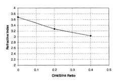
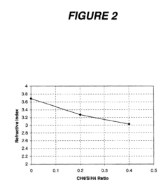
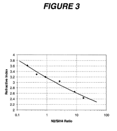
- The use of amorphous silicon (a-Si) materials, such as a-Si:H and a-Si:F based alloys, for waveguide formation in PICs, allowing for flexible index matching and low-loss coupling between active and passive components, achieved through Plasma Enhanced Chemical Vapor Deposition (PECVD) processes, which eliminates lattice match requirements and reduces optical absorption.
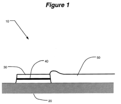
Photonic integrated circuit
PatentWO2025108755A1
Innovation
- A photonic integrated circuit design featuring a cladding layer with an opening for coupling with another photonic integrated circuit, utilizing silicon nitride-based waveguides and intermediary cladding layers to minimize coupling losses and enhance optical communication.
Miniaturization Strategies
Miniaturization is a critical challenge for integrating photonic circuits into wearable devices. Current photonic integrated circuits (PICs) require significant size reduction to meet the form factor demands of next-generation wearables. The industry is pursuing several promising approaches to address this challenge.
Material innovation represents a fundamental strategy for miniaturization. Silicon photonics has established itself as the dominant platform, but newer materials like silicon nitride, lithium niobate on insulator (LNOI), and indium phosphide offer superior properties for specific applications. These materials enable higher component density and reduced waveguide dimensions while maintaining optical performance. Particularly, thin-film lithium niobate allows for ultra-compact modulators that are 100 times smaller than conventional designs.
3D integration techniques are revolutionizing PIC miniaturization by exploiting vertical space. Multi-layer photonic platforms stack optical components in different layers, connected by optical vias or grating couplers. This approach has demonstrated up to 5x reduction in footprint compared to planar designs. Advanced 3D integration also facilitates heterogeneous integration of electronic and photonic components, crucial for wearable applications where space is at a premium.
Subwavelength structures and metamaterials represent another frontier in miniaturization. These engineered structures manipulate light at scales smaller than the wavelength, enabling unprecedented control over optical properties. Subwavelength gratings and photonic crystals can significantly reduce component sizes while enhancing functionality. Recent research has demonstrated metamaterial-based optical components with footprints reduced by up to 75% compared to conventional designs.
Novel waveguide geometries are also contributing to miniaturization efforts. Slot waveguides, photonic crystal waveguides, and plasmonics offer enhanced light confinement, allowing for tighter bends and more compact routing. Plasmonic waveguides, which leverage the interaction between light and free electrons at metal surfaces, can guide light in dimensions far below the diffraction limit, though they currently suffer from higher propagation losses.
Packaging innovations complete the miniaturization strategy landscape. Wafer-level packaging techniques, flip-chip bonding, and through-silicon vias enable more compact integration of photonic and electronic components. Advanced packaging approaches reduce the overall system footprint by up to 40% while improving thermal management and reliability, critical factors for wearable applications where devices operate in close proximity to the human body.
Power Efficiency Considerations
Power efficiency represents a critical consideration in the development of photonic integrated circuits (PICs) for next-generation wearable devices. The inherent energy constraints of wearable technology necessitate innovative approaches to minimize power consumption while maintaining high performance. Traditional electronic circuits in wearable devices typically consume between 10-100 mW of power, whereas photonic integrated solutions demonstrate potential to reduce this consumption by 30-50% through more efficient signal processing and data transmission.
The fundamental advantage of PICs in power efficiency stems from their ability to transmit and process signals using light rather than electrons. This optical approach eliminates resistive heating losses that plague electronic circuits, particularly in high-frequency applications. Recent research indicates that optical interconnects in PICs can achieve energy efficiencies below 1 pJ/bit, representing a significant improvement over electronic counterparts that typically operate at 5-10 pJ/bit.
Material selection plays a crucial role in optimizing power efficiency. Silicon photonics offers excellent integration capabilities but suffers from relatively high propagation losses. Alternative materials such as silicon nitride (Si₃N₄) and lithium niobate (LiNbO₃) demonstrate lower optical losses, with recent developments achieving propagation losses below 0.1 dB/cm. These advancements directly translate to lower power requirements for signal transmission across the photonic circuit.
Thermal management represents another significant challenge for PICs in wearable applications. Temperature fluctuations can alter the refractive index of photonic components, leading to wavelength shifts and performance degradation. Athermal design approaches, including the use of materials with compensating thermal coefficients and active temperature stabilization techniques, have demonstrated the ability to maintain stable operation across the 0-40°C temperature range typical for wearable devices while adding minimal power overhead.
Novel laser integration techniques are emerging as key enablers for power-efficient PICs. Heterogeneous integration of III-V materials on silicon platforms has produced lasers with threshold currents below 5 mA and wall-plug efficiencies exceeding 40%. These improvements directly impact the overall power budget of wearable PIC systems, as the laser typically accounts for 30-50% of the total power consumption in active photonic circuits.
Energy harvesting technologies present promising opportunities to supplement power requirements for PIC-based wearables. Recent demonstrations have shown that integrating photovoltaic cells directly onto the photonic chip can recover up to 15% of otherwise wasted optical power, creating a partial self-powering capability. This approach is particularly valuable for extending battery life in continuous monitoring applications such as health sensors and environmental detectors.
Unlock deeper insights with Patsnap Eureka Quick Research — get a full tech report to explore trends and direct your research. Try now!
Generate Your Research Report Instantly with AI Agent
Supercharge your innovation with Patsnap Eureka AI Agent Platform!