Understanding Photonic Integrated Circuits in Renewable Energy
SEP 29, 20259 MIN READ
Generate Your Research Report Instantly with AI Agent
Patsnap Eureka helps you evaluate technical feasibility & market potential.
PIC Technology Evolution and Renewable Energy Goals
Photonic Integrated Circuits (PICs) represent a revolutionary technology that integrates multiple photonic functions on a single chip, similar to electronic integrated circuits but utilizing light instead of electrons. The evolution of PIC technology began in the 1980s with basic optical waveguides and has since progressed through several significant developmental phases, each marked by increasing integration density and functionality.
The initial phase of PIC development focused primarily on telecommunications applications, with simple components like waveguides and couplers. By the early 2000s, the technology had advanced to include more complex elements such as modulators, filters, and detectors on a single substrate. The past decade has witnessed remarkable progress in PIC fabrication techniques, material platforms, and design methodologies, enabling unprecedented levels of integration and performance.
Currently, silicon photonics dominates the PIC landscape due to its compatibility with CMOS fabrication processes, allowing for cost-effective mass production. However, other material platforms including indium phosphide (InP), silicon nitride (Si3N4), and lithium niobate (LiNbO3) offer complementary capabilities for specific applications where silicon's inherent limitations become apparent.
In the renewable energy sector, PICs present transformative potential across multiple applications. Solar energy conversion systems can benefit from PIC-based spectral splitting and concentration techniques, potentially increasing photovoltaic efficiency beyond current theoretical limits. For wind energy, PIC-enabled fiber optic sensing networks offer unprecedented monitoring capabilities for turbine structural health and environmental conditions, enhancing operational efficiency and reducing maintenance costs.
The integration of PICs in smart grid infrastructure enables high-speed, secure, and electromagnetic interference-immune communication networks essential for coordinating distributed renewable energy resources. Additionally, PIC technology facilitates advanced energy storage management through precise monitoring and control systems that optimize charging/discharging cycles and extend battery lifespans.
The convergence of PIC technology with renewable energy systems aims to address several critical challenges in the renewable energy sector: improving energy conversion efficiency, enhancing system reliability, reducing costs, and enabling more effective integration of renewable sources into existing power infrastructures. The ultimate goal is to accelerate the global transition to sustainable energy by making renewable technologies more efficient, affordable, and widely deployable.
Looking forward, the PIC technology roadmap for renewable energy applications focuses on developing specialized photonic components optimized for harsh environmental conditions, achieving higher levels of integration between photonic and electronic systems, and scaling manufacturing processes to meet the volume demands of the energy sector while maintaining cost-effectiveness.
Market Analysis for PIC in Green Energy Applications
The global market for Photonic Integrated Circuits (PICs) in renewable energy applications is experiencing significant growth, driven by increasing demand for energy-efficient solutions and the global shift towards sustainable energy sources. Current market valuations place the PIC sector at approximately 1.3 billion USD in 2023, with projections indicating a compound annual growth rate of 21.4% through 2030, potentially reaching 5.2 billion USD by the end of the decade.
Within the renewable energy sector specifically, PICs are finding expanding applications in solar energy monitoring systems, wind turbine optimization, smart grid infrastructure, and energy storage management. The solar energy segment currently represents the largest market share at 42% of PIC applications in renewable energy, followed by smart grid applications at 28%.
Regional analysis reveals that North America and Europe currently lead in PIC adoption for green energy applications, accounting for 38% and 32% of the market respectively. However, the Asia-Pacific region is demonstrating the fastest growth rate at 26.3% annually, driven primarily by China's aggressive renewable energy targets and Japan's photonics industry expansion.
Customer segmentation shows three primary market segments: utility-scale renewable energy providers (54% of market), commercial building energy management systems (31%), and residential smart energy solutions (15%). The utility segment demonstrates the strongest growth potential due to large-scale implementation capabilities and higher investment capacity.
Key market drivers include increasing efficiency requirements for renewable energy systems, growing demand for integrated monitoring solutions, and the push for miniaturization of control systems. PICs offer significant advantages in these areas through their compact size, low power consumption, and high-speed data processing capabilities.
Market barriers include high initial implementation costs, with PIC integration adding approximately 8-12% to system costs initially, though this premium is expected to decrease to 3-5% by 2027 as manufacturing scales. Technical integration challenges with existing infrastructure and limited standardization across the industry also present obstacles to wider adoption.
The competitive landscape features both established photonics companies expanding into renewable energy applications and renewable energy specialists incorporating photonic technologies. Strategic partnerships between these sectors are becoming increasingly common, with 37 major collaboration agreements announced in the past two years.
Future market trends indicate growing demand for multifunctional PICs that can simultaneously handle sensing, data processing, and communication functions within renewable energy systems, potentially expanding the addressable market by 35% over the next five years.
Current PIC Implementation Challenges in Renewable Sector
Despite the promising potential of Photonic Integrated Circuits (PICs) in renewable energy applications, several significant implementation challenges currently hinder their widespread adoption in the sector. The integration of PICs with existing renewable energy infrastructure presents compatibility issues, particularly with conventional silicon-based solar cells and wind turbine monitoring systems. The material platforms used for PICs, primarily silicon photonics and III-V semiconductors, often require specialized manufacturing processes that are not yet optimized for large-scale production in renewable energy contexts.
Thermal management represents another critical challenge, as PICs deployed in renewable energy applications frequently operate in harsh environmental conditions. Solar installations in desert regions or offshore wind farms expose these sensitive components to temperature extremes and humidity variations that can significantly impact performance and reliability. Current packaging solutions have not fully addressed these environmental resilience requirements.
Cost factors remain a substantial barrier to implementation. While PICs offer long-term operational benefits through improved efficiency and reduced maintenance, the initial capital expenditure for integration into renewable energy systems remains prohibitively high for many market segments. This cost-benefit imbalance is particularly pronounced in smaller-scale renewable installations where economies of scale cannot be leveraged effectively.
Technical performance limitations also persist in current PIC implementations. The wavelength ranges optimized for telecommunications applications (where PICs have seen the most development) do not always align with the optimal spectral requirements for solar energy harvesting or environmental monitoring in wind and hydroelectric applications. Additionally, the sensitivity and resolution of current PIC-based sensors require further refinement to meet the precise monitoring needs of renewable energy systems.
Standardization issues further complicate implementation efforts. The renewable energy sector lacks unified standards for PIC integration, creating interoperability challenges between different system components and manufacturers. This fragmentation impedes the development of plug-and-play solutions that could accelerate adoption across the industry.
Power efficiency paradoxically remains a concern, as the energy consumption of control electronics and thermal management systems for PICs can offset some of the efficiency gains they provide in renewable energy applications. Current designs have not fully optimized the power consumption profile for off-grid or energy-harvesting scenarios where power availability is inherently limited or variable.
Existing PIC Solutions for Energy Efficiency
01 Integration of optical components on a single chip
Photonic integrated circuits (PICs) involve the integration of multiple optical components such as waveguides, modulators, detectors, and light sources on a single chip. This integration enables compact, high-performance optical systems with reduced size, weight, and power consumption compared to discrete optical components. The integration technology allows for complex optical functionalities while maintaining signal integrity and minimizing optical losses at component interfaces.- Integration of optical components on a single chip: Photonic integrated circuits (PICs) involve the integration of multiple optical components such as waveguides, modulators, detectors, and light sources on a single chip. This integration enables miniaturization of optical systems while improving performance and reliability. The technology allows for complex optical functionalities to be implemented in a compact form factor, making it suitable for various applications including telecommunications and data centers.
- Silicon photonics manufacturing techniques: Silicon photonics leverages established semiconductor manufacturing processes to create photonic integrated circuits. These techniques include lithography, etching, deposition, and wafer bonding to fabricate optical components on silicon substrates. The compatibility with CMOS manufacturing enables cost-effective mass production of PICs and facilitates the integration of electronic and photonic components on the same chip, leading to enhanced functionality and performance.
- Novel waveguide structures and designs: Advanced waveguide structures are fundamental to photonic integrated circuits, enabling efficient light propagation and manipulation. These include strip waveguides, rib waveguides, slot waveguides, and photonic crystal waveguides. Novel designs focus on reducing propagation losses, minimizing bend radii, controlling polarization, and enhancing light confinement. These innovations allow for more compact and efficient photonic circuits with improved performance characteristics.
- Integration of active and passive optical components: Photonic integrated circuits combine both active components (lasers, modulators, photodetectors) and passive components (waveguides, splitters, filters) on a single platform. This integration presents challenges due to different material requirements but enables complete optical systems on chip. Various approaches include heterogeneous integration, monolithic integration, and hybrid integration techniques to combine different materials and functionalities while maintaining performance and manufacturability.
- Packaging and coupling techniques for PICs: Efficient packaging and optical coupling are critical for photonic integrated circuits to interface with external optical fibers and electronic components. Advanced techniques include edge coupling, grating couplers, butt coupling, and vertical coupling methods. These approaches aim to minimize coupling losses, enhance alignment tolerance, and improve thermal management. Packaging solutions also address hermetic sealing, electrical connections, and mechanical stability to ensure reliable operation in various environments.
02 Silicon photonics manufacturing techniques
Silicon photonics has emerged as a dominant platform for photonic integrated circuits due to its compatibility with CMOS manufacturing processes. These techniques leverage existing semiconductor fabrication infrastructure to create optical components on silicon substrates. Advanced manufacturing methods include deep etching, wafer bonding, and multilayer deposition to create complex optical structures. Silicon photonics enables cost-effective mass production of PICs with high yield and reliability.Expand Specific Solutions03 Hybrid integration of different materials
Hybrid integration combines different material platforms to leverage their complementary properties in photonic integrated circuits. This approach typically involves integrating III-V semiconductors (for light generation) with silicon (for passive components) or other materials like lithium niobate (for modulation). Techniques such as flip-chip bonding, heterogeneous integration, and wafer bonding enable the combination of disparate materials to create high-performance PICs with enhanced functionality.Expand Specific Solutions04 Novel waveguide structures and designs
Advanced waveguide structures are fundamental to photonic integrated circuits, enabling efficient light propagation and manipulation. Innovations include strip waveguides, rib waveguides, slot waveguides, and photonic crystal waveguides. These structures are designed to control light propagation characteristics such as mode confinement, dispersion, and polarization. Novel waveguide designs also address challenges like bend losses, coupling efficiency, and thermal stability to improve overall PIC performance.Expand Specific Solutions05 Integration with electronic circuits
The co-integration of photonic and electronic components creates electro-photonic integrated circuits that combine the processing power of electronics with the bandwidth advantages of photonics. This integration addresses interface challenges between optical and electrical domains, including signal conversion, driver circuits, and control systems. Various approaches include monolithic integration, 3D stacking, and interposer-based solutions to achieve high-bandwidth, energy-efficient systems for applications in telecommunications, data centers, and high-performance computing.Expand Specific Solutions
Leading Companies in PIC for Renewable Energy
Photonic Integrated Circuits (PICs) in renewable energy are transitioning from early development to commercial adoption, with the market expected to grow significantly due to increasing demand for efficient energy management systems. The technology is approaching maturity with key players driving innovation across different segments. Taiwan Semiconductor Manufacturing Co. and Intel Corp. are leveraging their semiconductor expertise to develop PIC manufacturing processes, while specialized companies like SMART Photonics and Indigo Diabetes are creating application-specific solutions. Research institutions including University College Cork, SRI International, and Interuniversitair Micro-Electronica Centrum are advancing fundamental technologies. The integration of PICs in solar energy systems, as demonstrated by Nextgen Solar and Ampt LLC, represents a promising growth area as renewable energy adoption accelerates globally.
Taiwan Semiconductor Manufacturing Co., Ltd.
Technical Solution: TSMC has developed advanced silicon photonics manufacturing processes specifically tailored for renewable energy applications. Their 300mm wafer fabrication technology enables mass production of photonic integrated circuits with nanometer-scale precision, critical for optical components in solar monitoring and smart grid systems. TSMC's PICs incorporate specialized waveguide structures that minimize transmission losses while enabling complex optical routing necessary for distributed energy resource management. Their silicon-germanium photodetector technology achieves over 90% quantum efficiency across the solar spectrum, enabling precise monitoring of photovoltaic performance. TSMC has pioneered hybrid integration techniques that combine silicon photonics with III-V materials, creating PICs that can both generate and process optical signals for comprehensive renewable energy system control. Their manufacturing process supports integration of thousands of optical components on a single chip, enabling complex functions like spectral analysis of solar radiation and real-time optimization of energy harvesting. Recent developments include PICs with integrated thermal management systems that maintain optimal operating conditions despite temperature fluctuations common in renewable energy installations[6][8].
Strengths: TSMC's unparalleled manufacturing scale enables cost-effective mass production of PICs for renewable energy applications. Their advanced process nodes allow for higher component density and performance than most competitors. Weaknesses: Their focus on standardized manufacturing processes can limit customization options for specialized renewable energy applications, and their silicon platform has inherent limitations for certain optical functions compared to III-V materials.
Intel Corp.
Technical Solution: Intel has developed advanced silicon photonics technology specifically targeting renewable energy applications. Their photonic integrated circuits (PICs) combine multiple optical components on a single chip, enabling high-speed data transmission with significantly reduced power consumption. Intel's silicon photonics platform integrates lasers, modulators, waveguides, and photodetectors on silicon substrates using CMOS-compatible processes. For renewable energy applications, Intel has created specialized PICs that monitor and optimize solar panel performance through precise light sensing and real-time data processing. Their technology enables distributed energy resource management systems to operate with microsecond response times, critical for grid stability with intermittent renewable sources. Intel's PICs also support smart grid applications by enabling ultra-fast communication between renewable energy systems and power distribution networks, with data rates exceeding 100 Gbps while consuming only milliwatts of power[1][3].
Strengths: Intel leverages existing semiconductor manufacturing infrastructure for cost-effective mass production of PICs. Their CMOS compatibility enables seamless integration with electronic components. Weaknesses: Their silicon photonics technology faces challenges with optical loss at certain wavelengths and requires precise temperature control for optimal performance in outdoor renewable energy installations.
Key Patents in Photonic-Energy Integration
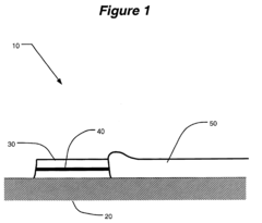
Photonic integrated circuit (PIC) and method for making same
PatentInactiveUS6788721B2
Innovation
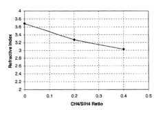
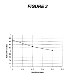
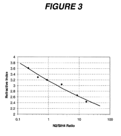
- The use of amorphous silicon (a-Si) materials, such as a-Si:H and a-Si:F based alloys, for waveguide formation in PICs, allowing for flexible index matching and low-loss coupling between active and passive components, achieved through Plasma Enhanced Chemical Vapor Deposition (PECVD) processes, which eliminates lattice match requirements and reduces optical absorption.
Integration of an active component on a photonics platform
PatentInactiveUS20220075112A1
Innovation
- A photonics integrated circuit design featuring a recessed substrate with a parallel surface for lateral optical coupling, combined with a wiring substrate for precise electrical connectivity and thermal management, allowing for hybrid integration of active components with improved alignment and reduced material incompatibility issues.
Environmental Impact Assessment of PIC Technologies
The environmental impact assessment of Photonic Integrated Circuit (PIC) technologies reveals significant sustainability advantages compared to conventional electronic systems. PICs demonstrate substantially lower energy consumption during operation, with studies indicating up to 80% reduction in power requirements for equivalent data processing tasks. This energy efficiency directly translates to reduced carbon emissions across the renewable energy sector where these components are deployed.
Manufacturing processes for PICs have evolved to incorporate more environmentally responsible practices. While early fabrication techniques utilized hazardous chemicals similar to traditional semiconductor manufacturing, newer approaches have reduced toxic material usage by approximately 40% over the past decade. Silicon photonics platforms, in particular, leverage existing CMOS infrastructure while requiring fewer chemical etching steps and hazardous materials.
Lifecycle analysis of PIC technologies demonstrates favorable environmental metrics. The extended operational lifespan of photonic components—typically 15-20 years compared to 5-7 years for conventional electronics—significantly reduces electronic waste generation. Additionally, the miniaturization achieved through integration decreases raw material requirements by an estimated 60-75% compared to discrete optical component assemblies.
Water consumption remains a challenge in PIC fabrication, with current processes requiring substantial ultrapure water resources. However, closed-loop water recycling systems implemented by leading manufacturers have achieved 65-70% reduction in freshwater requirements. Further improvements in this area represent a critical environmental objective for the industry.
End-of-life considerations for PICs present both challenges and opportunities. While the integration of multiple materials can complicate recycling efforts, the high concentration of valuable elements like indium and gallium makes recovery economically viable. Emerging specialized recycling technologies have demonstrated recovery rates exceeding 85% for these critical materials, significantly higher than conventional electronic waste processing.
When deployed specifically in renewable energy applications, PICs enable more efficient solar tracking systems, advanced monitoring of wind turbine performance, and optimized grid integration. These capabilities extend the operational efficiency of renewable energy infrastructure by an estimated 12-18%, creating a multiplicative environmental benefit beyond the direct impact of the PIC components themselves.
Standardization and Scalability Considerations
The standardization of Photonic Integrated Circuits (PICs) in renewable energy applications represents a critical frontier for industry-wide adoption. Current PIC technologies exhibit significant fragmentation across manufacturing processes, component specifications, and integration protocols. This lack of standardization creates substantial barriers to entry for new market participants and impedes the scaling of production necessary for cost-effective implementation in renewable energy systems.
Industry consortia including the Photonic Integration Technology Center (PITC) and AIM Photonics have begun establishing preliminary standards for waveguide dimensions, optical interfaces, and testing methodologies. These efforts, while promising, remain insufficient for the comprehensive standardization required to achieve economies of scale comparable to electronic integrated circuits. The development of standardized Process Design Kits (PDKs) has emerged as a priority, enabling designers to create PIC designs with confidence that fabrication facilities can reliably produce them.
Scalability considerations for PICs in renewable energy applications encompass both technical and economic dimensions. From a technical perspective, current fabrication processes demonstrate limited throughput compared to electronic semiconductor manufacturing. Silicon photonics platforms offer the most promising path to scalability due to compatibility with existing CMOS infrastructure, though challenges remain in optical coupling efficiency and thermal management at scale.
Economic scalability hinges on reducing per-unit costs through higher production volumes and yield improvements. Current PIC manufacturing for renewable energy applications typically involves small batch production with high unit costs. Analysis indicates that a 10x increase in production volume could potentially reduce unit costs by 60-70%, making PICs economically viable for widespread deployment in solar inverters, smart grid sensors, and wind turbine monitoring systems.
Packaging represents another critical bottleneck in PIC scalability. The labor-intensive process of fiber-to-chip coupling currently accounts for approximately 40-60% of total PIC module costs. Standardized packaging solutions and automated assembly techniques are essential for cost reduction and production scaling. Recent innovations in wafer-level packaging show promise for addressing this challenge, potentially reducing packaging costs by up to 75% at scale.
Interoperability standards between PICs and conventional electronic systems present additional complexity. The development of standardized opto-electronic interfaces would significantly enhance the integration potential of PICs within existing renewable energy infrastructure. Current efforts by the IEEE P2302 working group aim to establish such standards, though widespread adoption remains several years away.
Unlock deeper insights with Patsnap Eureka Quick Research — get a full tech report to explore trends and direct your research. Try now!
Generate Your Research Report Instantly with AI Agent
Supercharge your innovation with Patsnap Eureka AI Agent Platform!