

Photonic Integrated Circuits: Breakthroughs in Optical Computing
SEP 29, 20259 MIN READ
Generate Your Research Report Instantly with AI Agent
Patsnap Eureka helps you evaluate technical feasibility & market potential.
PIC Evolution and Objectives
Photonic Integrated Circuits (PICs) represent a revolutionary advancement in computing technology, evolving from the convergence of photonics and electronics. The journey began in the 1980s with rudimentary optical waveguides on silicon substrates, progressing through significant milestones including the development of silicon photonics in the early 2000s, which enabled the integration of multiple optical components on a single chip.
The evolution of PICs has been characterized by continuous improvements in integration density, performance, and functionality. Early PICs could only integrate a few components with limited functionality, whereas modern PICs can incorporate thousands of optical elements including lasers, modulators, detectors, and waveguides on a single chip. This progression mirrors the evolution of electronic integrated circuits but faces unique challenges related to light manipulation at the nanoscale.
Recent technological breakthroughs have accelerated PIC development, particularly in materials science with the introduction of novel materials like lithium niobate on insulator (LNOI), indium phosphide, and silicon nitride. These materials offer superior optical properties, enabling higher performance and more diverse applications. Additionally, advancements in fabrication techniques, including nanoimprint lithography and 3D integration methods, have significantly enhanced manufacturing capabilities.
The primary objective of PIC technology in optical computing is to overcome the limitations of electronic computing, particularly regarding speed, energy efficiency, and bandwidth. Electronic systems face fundamental physical constraints due to heat generation and signal delay, which optical systems can potentially circumvent. PICs aim to leverage the inherent advantages of light—including parallel processing capabilities, minimal heat generation, and ultra-fast signal propagation—to create computing systems that outperform their electronic counterparts.
Looking forward, the technological trajectory of PICs is focused on achieving several critical objectives: increasing integration density to accommodate more components per chip; improving coupling efficiency between optical and electronic domains; enhancing manufacturing scalability to reduce costs; and developing standardized design platforms to accelerate innovation and adoption.
The ultimate goal is to establish PICs as a mainstream technology for next-generation computing systems, capable of addressing complex computational problems that are currently intractable with conventional electronic approaches. This includes applications in quantum computing, artificial intelligence, and high-performance computing where the parallel processing capabilities of light can provide exponential performance improvements.
As the technology continues to mature, researchers are increasingly focusing on hybrid electronic-photonic systems that leverage the strengths of both domains, creating a pathway toward practical optical computing solutions that can be integrated with existing electronic infrastructure.
Optical Computing Market Analysis
The optical computing market is experiencing unprecedented growth, driven by the increasing limitations of traditional electronic computing systems and the rising demand for faster data processing capabilities. Current market valuations place the global optical computing sector at approximately $1.2 billion as of 2023, with projections indicating a compound annual growth rate (CAGR) of 26.8% through 2030, potentially reaching $6.5 billion by the end of the decade.
The demand for optical computing solutions is primarily fueled by data-intensive applications across multiple sectors. Cloud service providers and hyperscale data centers represent the largest market segment, accounting for nearly 38% of current demand, as they seek to overcome bandwidth bottlenecks and reduce energy consumption in their massive operations. Financial services follow closely at 22%, where high-frequency trading and complex risk calculations require ultra-low latency processing capabilities that photonic integrated circuits can deliver.
Telecommunications and networking equipment manufacturers constitute approximately 18% of the market, as they integrate optical computing components into next-generation infrastructure to handle exponentially growing data traffic. The artificial intelligence and machine learning sector, though currently representing only 12% of the market, is expected to be the fastest-growing segment with a projected CAGR of 34.2%, driven by the inherent advantages of optical computing in parallel processing for neural networks.
Geographically, North America leads the market with approximately 42% share, followed by Asia-Pacific at 31%, Europe at 21%, and the rest of the world at 6%. However, the Asia-Pacific region is expected to witness the highest growth rate, particularly in China, Japan, and South Korea, where significant investments in photonic technology research and manufacturing capabilities are being made.
The market is also segmented by component type, with optical processors representing 35% of the market, followed by optical interconnects (28%), optical memory devices (20%), and programming and interface solutions (17%). The integration of these components into complete photonic computing systems represents the highest value-added segment of the market.
Customer adoption patterns reveal a transition from experimental implementations to production-scale deployments, particularly in specialized computing tasks where optical solutions demonstrate clear advantages. Market surveys indicate that 63% of enterprise technology decision-makers are either actively evaluating or planning to evaluate optical computing solutions within the next three years, signaling strong future demand potential.
PIC Technology Landscape and Barriers
The global landscape of Photonic Integrated Circuits (PICs) has evolved significantly over the past decade, with major research institutions and corporations across North America, Europe, and Asia making substantial investments. The United States maintains leadership through DARPA-funded initiatives and corporate R&D from Intel, IBM, and startups like Lightmatter. Europe has established strong research clusters in the Netherlands, Germany, and the UK, with organizations like IMEC and Fraunhofer Institute driving innovation. In Asia, China has rapidly accelerated its PIC development through national strategic initiatives, while Japan and Singapore maintain specialized expertise in specific PIC applications.
Despite this progress, the PIC industry faces significant technical barriers that impede widespread commercial adoption. Integration density remains a fundamental challenge, with current photonic components still orders of magnitude larger than their electronic counterparts. This size disparity limits the computational power that can be packed into a single chip. Material compatibility presents another major hurdle, as silicon photonics—while leveraging existing CMOS infrastructure—suffers from inherent limitations in light emission and modulation efficiency.
Thermal management represents a critical challenge for optical computing applications. Temperature fluctuations significantly impact optical properties, requiring precise thermal control systems that add complexity and power consumption. Manufacturing scalability also remains problematic, with current fabrication processes lacking the maturity and yield rates of traditional semiconductor manufacturing, resulting in higher costs and limited production capacity.
The coupling efficiency between optical fibers and photonic chips continues to be a technical bottleneck, with coupling losses reducing overall system performance. This issue is particularly acute in data center applications where thousands of connections may be required. Additionally, the lack of standardized design tools and PDKs (Process Design Kits) comparable to those in the electronic industry hampers development cycles and increases costs.
Power efficiency presents another significant barrier. While optical computing theoretically offers energy advantages over electronic systems, current implementations often require power-hungry conversions between optical and electrical domains, negating much of the potential benefit. Finally, the industry faces a talent shortage, with limited educational programs specifically focused on photonic integration, creating a gap between research advancements and commercial implementation capabilities.
These technical barriers collectively form a complex landscape that requires coordinated efforts across academia, industry, and government to overcome. Recent breakthroughs in heterogeneous integration and novel materials like lithium niobate on insulator (LNOI) show promise in addressing some of these challenges, potentially accelerating the path toward practical optical computing systems.
Current PIC Architectures
01 Integration of novel materials in photonic integrated circuits
Recent breakthroughs in photonic integrated circuits (PICs) involve the incorporation of novel materials that enhance performance and functionality. These materials include III-V semiconductors, silicon nitride, and other advanced compounds that enable improved light generation, modulation, and detection. The integration of these materials with traditional silicon platforms has led to hybrid PICs with superior optical properties, increased bandwidth, and enhanced efficiency for various applications including telecommunications and data processing.- Integration of novel materials in photonic integrated circuits: Recent breakthroughs in photonic integrated circuits (PICs) involve the integration of novel materials that enhance performance and functionality. These materials include silicon nitride, indium phosphide, and other compound semiconductors that offer improved light manipulation capabilities. The integration of these materials allows for better optical properties, reduced losses, and enhanced efficiency in photonic circuits, enabling applications in telecommunications, sensing, and quantum computing.
- Advanced waveguide structures and designs: Innovations in waveguide structures represent significant breakthroughs in photonic integrated circuits. These include novel geometries, multi-layer waveguides, and specialized coupling structures that improve light propagation and minimize losses. Advanced waveguide designs enable better control of optical modes, enhanced light confinement, and more efficient routing of optical signals across the photonic chip, leading to improved performance in data transmission and processing applications.
- Integration of active and passive components: A major breakthrough in photonic integrated circuits involves the seamless integration of both active components (lasers, modulators, detectors) and passive components (waveguides, splitters, filters) on a single chip. This heterogeneous integration approach combines different materials and fabrication techniques to create complete optical systems on chip. The integration reduces coupling losses, decreases footprint, improves reliability, and enables complex functionalities for applications in optical communications, sensing, and computing.
- Advanced manufacturing techniques for photonic circuits: Breakthroughs in manufacturing techniques have revolutionized photonic integrated circuit production. These include advanced lithography processes, 3D integration methods, and novel etching techniques that enable more precise fabrication of nanoscale photonic structures. These manufacturing innovations allow for higher component density, better yield, improved reproducibility, and the ability to create more complex photonic architectures, facilitating mass production of high-performance photonic chips.
- Photonic-electronic integration and co-design: Recent breakthroughs focus on the integration of photonic and electronic components on the same substrate, creating electro-photonic integrated circuits. This co-integration approach combines the high-speed data processing capabilities of photonics with the computational power of electronics. Advanced co-design methodologies enable optimized interfaces between optical and electrical domains, reducing power consumption and improving overall system performance for applications in data centers, high-performance computing, and telecommunications networks.
02 Advanced waveguide structures and optical coupling techniques
Significant advancements have been made in waveguide structures and optical coupling methods for photonic integrated circuits. These innovations include improved grating couplers, edge couplers, and novel waveguide geometries that minimize losses and enhance light propagation. The development of efficient coupling between different optical components and between optical fibers and chips has been crucial for improving overall PIC performance, enabling more complex integrated photonic systems with higher data transmission rates.Expand Specific Solutions03 On-chip optical signal processing and computing
Breakthroughs in on-chip optical signal processing and computing have revolutionized photonic integrated circuits. These advancements include the development of optical logic gates, all-optical switches, and photonic neural networks that can perform computing operations using light rather than electrons. By leveraging the parallelism and speed of light, these technologies offer significant advantages in terms of processing speed, energy efficiency, and bandwidth compared to traditional electronic circuits, opening new possibilities for optical computing and artificial intelligence applications.Expand Specific Solutions04 Integration of lasers and light sources on silicon platforms
A major breakthrough in photonic integrated circuits has been the successful integration of lasers and light sources directly on silicon platforms. This includes heterogeneous integration of III-V lasers, the development of silicon-compatible light emitters, and novel approaches to overcome the indirect bandgap limitation of silicon. These advancements enable fully integrated photonic systems on a single chip, reducing size, cost, and power consumption while improving reliability for applications in telecommunications, sensing, and quantum information processing.Expand Specific Solutions05 Photonic integrated circuits for quantum technologies
Recent breakthroughs have enabled the development of photonic integrated circuits specifically designed for quantum technologies. These include on-chip generation, manipulation, and detection of quantum states of light, such as single photons and entangled photon pairs. The integration of quantum components on photonic chips facilitates scalable quantum information processing, quantum key distribution for secure communications, and quantum sensing applications. These advancements represent a significant step toward practical quantum computing and quantum communication networks.Expand Specific Solutions
Leading PIC Industry Players
Photonic Integrated Circuits (PICs) are emerging as a transformative technology in optical computing, currently in the early growth phase with significant market potential. The global PIC market is expanding rapidly, driven by demands for higher computing speeds and energy efficiency. Leading semiconductor manufacturers like TSMC and Intel are investing heavily in this space, while specialized players such as Lightmatter and PsiQuantum are developing breakthrough photonic solutions for AI and quantum computing applications. Academic-industry partnerships involving MIT, Caltech, and Shanghai Jiao Tong University are accelerating innovation. Though still evolving toward full commercial maturity, PICs are advancing quickly with companies like Shanghai Xizhi demonstrating photonic chip prototypes achieving processing accuracy comparable to electronic chips, signaling the technology's readiness for broader adoption.
Taiwan Semiconductor Manufacturing Co., Ltd.
Technical Solution: TSMC has developed advanced silicon photonics integration platforms that combine optical components with high-performance CMOS electronics. Their technology enables the fabrication of complex photonic integrated circuits on 300mm silicon wafers using their established semiconductor manufacturing processes. TSMC's silicon photonics platform features low-loss silicon nitride and silicon waveguides, high-speed germanium photodetectors, efficient electro-optic modulators, and advanced passive components like wavelength multiplexers and optical power splitters[13]. A key innovation is their 3D integration approach that stacks photonic layers with electronic CMOS layers using through-silicon vias (TSVs) and copper pillar bonding to achieve unprecedented integration density while maintaining optical performance[14]. TSMC has demonstrated photonic transceivers operating at 224 Gbps per wavelength channel with multiple channels per chip, enabling aggregate bandwidths exceeding 1.6 Tbps in a single package. Their manufacturing capabilities allow for wafer-scale testing and production of photonic integrated circuits with nanometer-precision alignment of optical components[15].
Strengths: Unparalleled semiconductor manufacturing expertise and infrastructure that can be applied to photonic integration; established quality control and yield management systems; ability to scale production to meet commercial demand. Weaknesses: Primary business remains electronic semiconductor manufacturing; less experience with optical design compared to specialized photonics companies; relatively conservative approach to adopting new materials systems required for some photonic applications.
Intel Corp.
Technical Solution: Intel has developed silicon photonics technology that integrates lasers directly onto silicon chips, enabling high-speed optical interconnects for data centers and high-performance computing. Their platform combines III-V materials with silicon using advanced wafer bonding techniques to create integrated laser sources, modulators, and photodetectors on a single chip. Intel's 400G and 800G transceivers leverage this technology to achieve data rates up to 224 Gbps per channel[1]. Their recent breakthrough includes a fully integrated eight-channel silicon photonic transmitter with hybrid III-V/Si lasers and high-speed silicon-germanium modulators, demonstrating aggregate bandwidths exceeding 400 Gbps[2]. Intel also pioneered programmable photonic integrated circuits (PICs) that can be reconfigured for different optical computing functions, similar to FPGAs in electronic computing, allowing for more versatile optical processing applications[3].
Strengths: Industry-leading manufacturing capabilities and established silicon fabrication infrastructure that can be leveraged for photonic integration; extensive intellectual property portfolio in silicon photonics. Weaknesses: Relatively higher power consumption compared to specialized photonic startups; primary focus remains on electronic computing with photonics as complementary technology rather than core business.
Key PIC Innovations and Patents
Method and structure to incorporate multiple low loss photonic circuit components
PatentPendingUS20230366913A1
Innovation
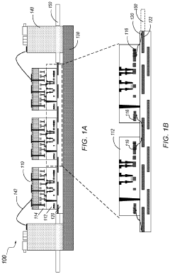
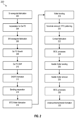
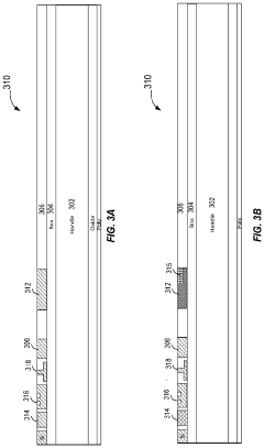
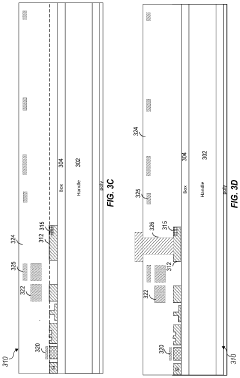
- A photonic integrated circuit (PIC) is designed using semiconductor processing technology, incorporating silicon nitride waveguides, Pockels effect optical phase shifters, superconductive nanowire single photon detectors, and optical isolation structures, with components like BaTiO3 optical phase shifters and Ge photodiodes, and employing techniques like high-temperature annealing to reduce waveguide losses and integrate various components on a single wafer or die.
Photonic device, system and method of making same
PatentActiveUS11899240B2
Innovation
- The development of a photonic device with vertically stacked waveguide layers allows for optical power exchange between different photonic layers, enabling the creation of a 3D photonic neural network with reduced chip size, lower fabrication costs, and enhanced computation density.
Material Advancements for PICs
Material advancements represent a critical frontier in the evolution of Photonic Integrated Circuits (PICs) for optical computing applications. Silicon has traditionally dominated the PIC landscape due to its compatibility with CMOS fabrication processes, enabling cost-effective integration with electronic components. However, silicon's inherent limitations—particularly its indirect bandgap preventing efficient light emission—have spurred research into alternative materials.
Group III-V compound semiconductors, including gallium arsenide (GaAs) and indium phosphide (InP), have emerged as promising alternatives due to their direct bandgap properties, enabling efficient light emission and detection. These materials demonstrate superior performance in active photonic components such as lasers and amplifiers, though integration challenges with silicon platforms remain significant.
Silicon nitride (Si3N4) has gained prominence for passive photonic components, offering lower propagation losses than silicon and broader operational wavelength ranges. Its transparency across visible and near-infrared spectra makes it particularly valuable for applications requiring precise light manipulation across multiple wavelengths.
Recent breakthroughs in heterogeneous integration techniques have enabled the combination of disparate materials on a single chip. Wafer bonding and epitaxial growth methods now allow the integration of III-V materials with silicon substrates, creating hybrid platforms that leverage the strengths of multiple materials while mitigating their individual limitations.
Two-dimensional materials represent the cutting edge of PIC material science. Graphene, with its exceptional electron mobility and broadband optical absorption, shows promise for ultrafast photodetectors and modulators. Transition metal dichalcogenides (TMDs) like MoS2 and WSe2 exhibit direct bandgaps at monolayer thickness, potentially enabling extremely compact light sources and detectors.
Phase-change materials such as Ge2Sb2Te5 (GST) have demonstrated remarkable potential for reconfigurable photonic devices. These materials can rapidly switch between amorphous and crystalline states with significantly different optical properties, enabling programmable photonic circuits that can be reconfigured post-fabrication.
Lithium niobate on insulator (LNOI) has reemerged as a compelling platform for PICs due to advances in thin-film fabrication techniques. Its strong electro-optic effect enables high-speed, low-power modulators essential for optical computing applications, while recent fabrication improvements have dramatically reduced previously prohibitive propagation losses.
These material advancements collectively address the fundamental challenges facing optical computing implementations, potentially enabling PICs with unprecedented performance in terms of speed, energy efficiency, and computational density. The continued development of novel materials and integration techniques remains essential for realizing the full potential of photonic integrated circuits in next-generation computing architectures.
Energy Efficiency Comparison
Energy efficiency represents a critical metric for evaluating the viability of photonic integrated circuits (PICs) in optical computing applications. Traditional electronic computing systems face significant energy constraints due to heat dissipation issues and increasing power demands. PICs offer a revolutionary alternative by utilizing photons instead of electrons as information carriers, resulting in substantially reduced energy consumption.
When comparing energy efficiency between electronic and photonic computing systems, PICs demonstrate remarkable advantages. Electronic systems typically consume energy in the range of picojoules per bit (pJ/bit), while advanced photonic systems can achieve femtojoule per bit (fJ/bit) levels—representing orders of magnitude improvement. This efficiency gain stems from the fundamental physics of photons, which do not generate resistive heating during signal transmission and can be multiplexed across multiple wavelengths.
Recent breakthroughs in PIC technology have further enhanced energy efficiency metrics. Silicon photonics platforms have achieved switching energies below 10 fJ/bit, while novel materials like lithium niobate on insulator (LNOI) demonstrate sub-femtojoule operations for certain computing functions. These improvements make optical computing increasingly competitive against traditional CMOS technology, particularly for data-intensive applications.
The energy advantage becomes particularly pronounced in data centers, where cooling costs often match or exceed direct computing power consumption. Thermal simulations indicate that large-scale PIC implementation could reduce cooling requirements by 30-45% compared to equivalent electronic systems. This translates to significant operational expenditure reductions and improved total cost of ownership for computing infrastructure.
Power scaling also favors photonic approaches. While electronic computing power consumption typically scales linearly or super-linearly with computational throughput, photonic systems can maintain near-constant power consumption across varying computational loads through wavelength division multiplexing techniques. This characteristic proves especially valuable for applications with fluctuating computational demands.
Despite these advantages, hybrid electro-photonic systems currently represent the most practical implementation path. The energy overhead of electro-optical and opto-electrical conversions remains a challenge, though recent integration advances have reduced this penalty significantly. Complete system-level analyses suggest that applications requiring high bandwidth and parallel processing capabilities benefit most from current PIC energy efficiency profiles.
Looking forward, emerging materials and architectural innovations promise to further widen the energy efficiency gap between photonic and electronic computing paradigms, potentially enabling entirely new classes of energy-constrained applications.
Unlock deeper insights with Patsnap Eureka Quick Research — get a full tech report to explore trends and direct your research. Try now!
Generate Your Research Report Instantly with AI Agent
Supercharge your innovation with Patsnap Eureka AI Agent Platform!