Why Are Photonic Integrated Circuits Critical for Modern Networks
SEP 29, 20259 MIN READ
Generate Your Research Report Instantly with AI Agent
Patsnap Eureka helps you evaluate technical feasibility & market potential.
Photonic Integration Background and Objectives
Photonic Integrated Circuits (PICs) represent a revolutionary advancement in optical communication technology, evolving from the foundational work in integrated optics during the 1970s. This evolution has been driven by the exponential growth in global data traffic, which traditional electronic systems increasingly struggle to accommodate. The fundamental principle behind PICs involves the integration of multiple photonic components onto a single chip, enabling light manipulation for data transmission, processing, and sensing applications.
The historical development of PICs has been marked by significant milestones, beginning with rudimentary waveguide structures and progressing to complex systems incorporating lasers, modulators, detectors, and multiplexers on a single substrate. The 1990s witnessed the first commercial applications in telecommunications, while the 2000s brought enhanced fabrication techniques that dramatically improved performance and reduced costs.
Current technological trends in photonic integration focus on several key areas: material platform diversification beyond traditional silicon and indium phosphide; increased integration density to accommodate more components per chip; improved coupling efficiency between optical and electronic domains; and enhanced manufacturing scalability to support mass production requirements.
The primary objective of modern PIC development is to address the bandwidth and energy efficiency limitations of conventional electronic circuits in network infrastructure. As data rates continue to escalate, electronic interconnects face fundamental physical constraints related to power consumption, heat dissipation, and signal integrity at high frequencies. Photonic integration offers a promising solution by leveraging light's inherent advantages: higher bandwidth, lower latency, and reduced power consumption per bit transmitted.
For modern networks specifically, PICs aim to enable terabit-per-second data transmission while simultaneously reducing energy consumption by orders of magnitude compared to electronic alternatives. This dual objective is critical as network operators face mounting pressure to support exponentially growing data demands while minimizing environmental impact and operational costs.
Additional technical goals include achieving higher levels of functional integration, improving reliability under varying environmental conditions, reducing form factors to accommodate space-constrained applications, and developing standardized interfaces for seamless integration with existing network infrastructure.
The convergence of these technological trajectories and objectives positions photonic integration as a cornerstone technology for next-generation network architectures, from metropolitan and long-haul telecommunications to data center interconnects and emerging edge computing applications. Understanding this background provides essential context for evaluating the critical role PICs play in addressing the fundamental challenges facing modern network infrastructure.
Market Demand Analysis for PIC-Based Networks
The global market for Photonic Integrated Circuits (PICs) in network applications is experiencing unprecedented growth, driven by the exponential increase in data traffic and connectivity demands. Current market projections indicate that the PIC market is expected to reach $3.5 billion by 2025, with a compound annual growth rate of approximately 25% between 2020-2025. This remarkable growth trajectory is primarily fueled by the telecommunications sector, which accounts for nearly 60% of the total market share.
The surging demand for PICs stems from several interconnected market factors. First, the explosive growth in internet traffic—with global IP traffic surpassing 4.8 zettabytes annually—has created an urgent need for higher bandwidth solutions that traditional electronic circuits cannot efficiently deliver. PICs offer the necessary capacity to handle this data deluge while maintaining signal integrity over longer distances.
Data center operators represent another significant market segment driving PIC adoption. With the shift toward hyperscale cloud computing architectures, these facilities require ultra-high-speed interconnects between and within data centers. Market research indicates that nearly 70% of data center operators plan to incorporate PIC-based solutions in their infrastructure upgrades within the next three years, recognizing the technology's ability to reduce power consumption while increasing data throughput.
The 5G and upcoming 6G network deployments constitute another substantial market driver. Telecommunications providers are investing heavily in network infrastructure that can support the promised multi-gigabit speeds and ultra-low latency. PIC-based transceivers and switches are becoming essential components in these next-generation networks, with the market for PIC-enabled 5G infrastructure expected to grow at 32% annually through 2026.
From a geographical perspective, North America currently leads the PIC market with approximately 40% share, followed by Asia-Pacific at 35% and Europe at 20%. However, the Asia-Pacific region is projected to witness the fastest growth rate, driven by massive telecommunications infrastructure investments in China, Japan, and South Korea.
Consumer demand for bandwidth-intensive applications like 4K/8K video streaming, virtual reality, and cloud gaming is creating additional market pressure for network upgrades. Industry surveys indicate that average household bandwidth requirements are doubling approximately every 18 months, necessitating fundamental improvements in network infrastructure that PICs can address.
The enterprise sector also shows strong demand signals, with financial services, healthcare, and manufacturing industries increasingly requiring ultra-low latency connections for time-sensitive applications like algorithmic trading, telemedicine, and industrial automation. These specialized applications represent premium market segments where the performance advantages of PIC-based networks justify their higher implementation costs.
PIC Technology Status and Challenges
Photonic Integrated Circuits (PICs) have reached a critical juncture in their technological evolution, with significant advancements achieved globally while facing persistent challenges that limit their widespread adoption. Currently, PICs have progressed from laboratory demonstrations to commercial deployment in telecommunications, data centers, and sensing applications, with integration densities reaching thousands of components on a single chip.
The global PIC market is experiencing rapid growth, with North America and Europe leading in research and development, while Asia is quickly emerging as a manufacturing powerhouse. Academic institutions like MIT, Caltech, and TU Eindhoven, alongside industrial giants such as Intel, Cisco, and Huawei, are driving innovation in this field. This geographical distribution creates a complex ecosystem of knowledge transfer and technological advancement.
Despite impressive progress, PICs face several significant technical challenges. Integration density remains limited compared to electronic integrated circuits, primarily due to the fundamental size constraints of optical waveguides and components. Current PIC platforms typically achieve component densities of 100-1000 elements per square centimeter, orders of magnitude lower than their electronic counterparts.
Material platform compatibility presents another major hurdle. Silicon photonics offers CMOS compatibility but suffers from indirect bandgap limitations for light sources. III-V semiconductors provide excellent light emission but at higher manufacturing costs. Hybrid integration approaches combining multiple material systems show promise but introduce complex fabrication challenges and potential reliability issues at interface points.
Coupling efficiency between optical fibers and PICs remains problematic, with typical coupling losses of 3-5 dB per connection point significantly impacting overall system performance. Various solutions including grating couplers, edge couplers, and spot-size converters have been developed, but each comes with trade-offs in bandwidth, polarization sensitivity, and fabrication complexity.
Thermal management represents another critical challenge as photonic components often exhibit temperature-dependent performance characteristics. Active temperature control systems add complexity, power consumption, and cost to PIC-based systems. Novel athermal designs and materials with reduced temperature sensitivity are under development but have not yet reached commercial maturity.
Manufacturing scalability and yield issues continue to constrain cost-effective mass production. Unlike electronic ICs with standardized processes, PIC fabrication often requires customized processes for different applications. Testing and packaging of PICs present additional complications, with current solutions being largely application-specific and difficult to standardize across the industry.
Current PIC Solutions for Network Applications
01 Integration of optical components on a single chip
Photonic integrated circuits (PICs) involve the integration of multiple optical components such as waveguides, modulators, detectors, and light sources on a single chip. This integration enables miniaturization of optical systems while maintaining or improving performance. The technology allows for complex optical functionalities in a compact form factor, reducing size, weight, and power consumption compared to discrete optical component assemblies.- Integration of optical components on a single chip: Photonic integrated circuits (PICs) involve the integration of multiple optical components such as waveguides, modulators, detectors, and light sources on a single chip. This integration enables compact, high-performance optical systems with reduced size, weight, and power consumption compared to discrete optical components. The integration technology allows for complex optical functionalities while maintaining signal integrity and reducing coupling losses between components.
- Silicon photonics manufacturing techniques: Silicon photonics leverages established semiconductor manufacturing processes to create photonic integrated circuits. These techniques include lithography, etching, deposition, and wafer bonding to fabricate optical structures on silicon substrates. The compatibility with CMOS fabrication enables cost-effective mass production of PICs and facilitates the integration of electronic and photonic components on the same chip, leading to enhanced functionality and performance for various applications.
- Novel waveguide structures and designs: Advanced waveguide structures are fundamental to photonic integrated circuits, enabling efficient light propagation and manipulation. These include strip waveguides, rib waveguides, slot waveguides, and photonic crystal waveguides, each offering specific advantages for different applications. Novel designs focus on minimizing propagation losses, controlling dispersion, enhancing mode confinement, and enabling efficient coupling between different optical components within the PIC.
- Integration of active and passive optical components: Modern photonic integrated circuits combine both active components (lasers, modulators, detectors) and passive components (waveguides, splitters, filters) on a single platform. This integration requires specialized techniques such as heterogeneous integration, wafer bonding, or monolithic growth to combine different material systems. The successful integration of these diverse components enables complete optical systems on chip for applications in telecommunications, sensing, and computing.
- Packaging and coupling techniques for PICs: Efficient packaging and coupling solutions are critical for connecting photonic integrated circuits to the outside world. These include fiber-to-chip coupling methods such as grating couplers, edge couplers, and spot-size converters that minimize insertion losses. Advanced packaging techniques address thermal management, hermetic sealing, and electrical connections while maintaining optical alignment. These solutions enable practical deployment of PICs in real-world applications while preserving their performance advantages.
02 Silicon photonics manufacturing techniques
Silicon photonics leverages established semiconductor manufacturing processes to create photonic integrated circuits. These techniques include lithography, etching, deposition, and wafer bonding to fabricate optical structures on silicon substrates. The compatibility with CMOS fabrication enables high-volume, cost-effective production of PICs with precise optical features at nanometer scale, facilitating integration with electronic components on the same chip.Expand Specific Solutions03 Optical interconnects for data communication
Photonic integrated circuits provide high-bandwidth, energy-efficient optical interconnects for data communication applications. These interconnects use light instead of electrical signals to transmit data between chips, boards, or systems, overcoming the bandwidth and power limitations of traditional copper interconnects. The technology enables higher data rates with lower latency and reduced power consumption, making it suitable for data centers, high-performance computing, and telecommunications networks.Expand Specific Solutions04 Integration of lasers and active components
Advanced techniques for integrating lasers and other active components into photonic integrated circuits are essential for creating fully functional optical systems. These methods include heterogeneous integration of III-V materials with silicon, monolithic integration approaches, and hybrid assembly techniques. The integration of light sources, amplifiers, and modulators with passive waveguide structures enables complete optical systems on a single chip for applications in sensing, communications, and computing.Expand Specific Solutions05 Specialized PIC designs for quantum and neuromorphic applications
Novel photonic integrated circuit designs are being developed for emerging applications in quantum information processing and neuromorphic computing. These specialized PICs incorporate structures for generating, manipulating, and detecting quantum states of light or implementing optical neural network architectures. The designs leverage unique properties of integrated photonics such as low loss, high coherence, and parallelism to enable quantum communication, quantum computing, and photonic neural networks with capabilities beyond conventional electronic systems.Expand Specific Solutions
Key Industry Players in Photonic Integration
Photonic Integrated Circuits (PICs) are emerging as critical components for modern networks, currently transitioning from early adoption to commercial growth phase. The global PIC market is expanding rapidly, projected to reach significant scale as data demands increase exponentially. Technologically, industry leaders are advancing at varying maturity levels: Intel, TSMC, and Infinera have established commercial PIC platforms, while Huawei, AMD, and Marvell are making substantial R&D investments. Academic institutions like Columbia University and Shanghai Jiao Tong University are pioneering next-generation PIC technologies. Companies like Xizhi Technology have demonstrated breakthrough prototypes achieving performance comparable to electronic chips. This competitive landscape reflects PICs' strategic importance in addressing bandwidth, energy efficiency, and latency challenges in modern network infrastructure, with both established semiconductor giants and specialized innovators driving advancement.
Intel Corp.
Technical Solution: Intel has developed a silicon photonics platform that integrates optical components with CMOS electronics on silicon wafers. Their technology focuses on high-volume manufacturing of integrated transceivers for data center interconnects and telecommunications networks. Intel's silicon photonics solutions incorporate integrated lasers, modulators, multiplexers, and photodetectors on a single chip, enabling data rates from 100G to 400G per module. Their manufacturing approach leverages existing semiconductor fabrication infrastructure, allowing for cost-effective scaling. Intel has recently demonstrated co-packaged optics that place optical I/O directly next to switch ASICs, reducing power consumption by up to 30% and increasing bandwidth density. Their technology roadmap includes plans for 800G and 1.6T optical connectivity solutions using advanced modulation formats and wavelength division multiplexing techniques.
Strengths: Leverages established semiconductor manufacturing expertise and infrastructure; integration with CMOS electronics enables lower-cost solutions; strong position in data center market. Weaknesses: Silicon's indirect bandgap requires hybrid integration of III-V materials for light sources, adding complexity; relatively newer entrant to the optical networking market compared to traditional players.
Huawei Technologies Co., Ltd.
Technical Solution: Huawei has developed an advanced silicon photonics platform called OptiXtreme that integrates multiple optical functions on a single chip for high-speed optical communications. Their PICs incorporate germanium photodetectors, silicon modulators, and hybrid III-V/silicon lasers to achieve data rates exceeding 800 Gbps per wavelength. Huawei's technology employs advanced multiplexing techniques including polarization, wavelength, and spatial division multiplexing to maximize bandwidth density. Their OptiX family of products utilizes these PICs for metro, long-haul, and submarine network applications, supporting flexible grid wavelength management and software-defined optical networking capabilities. Huawei has demonstrated coherent optical modules with integrated DSP ASICs that achieve spectral efficiencies approaching the Shannon limit while maintaining compact form factors suitable for next-generation network equipment.
Strengths: Comprehensive vertical integration from chips to systems enables optimized solutions; strong R&D investment in advanced modulation formats and DSP algorithms; established presence in global telecommunications infrastructure. Weaknesses: Geopolitical challenges limit market access in some regions; dependency on external foundries for some manufacturing processes.
Core PIC Technologies and Patents
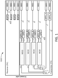
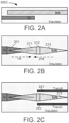
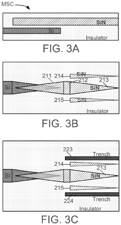
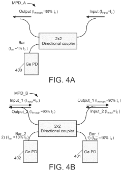
Silicon photonics integration circuit
PatentActiveUS20240045139A1
Innovation
- A silicon photonics integration circuit (SPIC) is developed on a single silicon-based wafer, incorporating novel mode size converters, high-performance silicon optical modulators, and Germanium-based high-speed photo diodes, along with low-loss passive waveguide devices, to enhance optical-electrical conversion efficiency and reduce power consumption.
Energy Efficiency Impact of PICs
The energy consumption of data centers and telecommunications networks has grown exponentially with the increasing demand for bandwidth and connectivity. Photonic Integrated Circuits (PICs) represent a transformative technology in addressing these energy challenges, offering significant advantages over traditional electronic solutions.
PICs fundamentally alter the energy equation in modern networks by leveraging light instead of electrons for data transmission and processing. While electronic circuits face inherent resistive losses that generate heat and consume power, photonic circuits can transmit signals with minimal energy loss across longer distances. Research indicates that PICs can achieve energy savings of 50-75% compared to electronic counterparts in high-bandwidth applications.
The power efficiency of PICs derives from several key mechanisms. First, optical interconnects eliminate the need for repeated signal regeneration and amplification required in electronic systems. Second, wavelength division multiplexing (WDM) implemented in PICs allows multiple data streams to be transmitted simultaneously on different wavelengths without proportional increases in power consumption. Third, the absence of resistive heating significantly reduces cooling requirements, which typically account for 30-40% of data center energy costs.
In practical deployments, silicon photonics-based transceivers have demonstrated energy efficiencies below 5 picojoules per bit, compared to 20-30 picojoules per bit for conventional solutions. This efficiency becomes increasingly critical as network traffic continues to grow at 25-30% annually while energy resources remain constrained.
The environmental impact of this improved efficiency is substantial. Conservative estimates suggest that widespread PIC adoption could reduce ICT-related carbon emissions by 3-5% globally by 2030. For hyperscale data center operators, this translates to potential energy cost savings of hundreds of millions of dollars annually while supporting sustainability initiatives.
Looking forward, emerging PIC technologies promise even greater efficiency gains. Heterogeneous integration combining different materials on a single chip platform may further reduce power requirements by 80-90% for specific applications. Additionally, co-packaged optics that place photonic elements directly alongside electronic processors minimize energy-intensive electrical-optical conversions.
As network demands continue to escalate with emerging technologies like 5G, IoT, and artificial intelligence, the energy efficiency advantages of PICs will likely become not merely beneficial but essential for sustainable network growth and operation.
Standardization Efforts in PIC Technology
Standardization efforts in the Photonic Integrated Circuit (PIC) industry have become increasingly vital as the technology matures and seeks broader commercial adoption. Several international organizations are actively developing standards to ensure interoperability, reliability, and cost-effectiveness across the PIC ecosystem. The Joint European Platform for Photonic Integration of Components and Circuits (JePPIX) has been instrumental in establishing design rules and process design kits (PDKs) that enable fabless development models similar to those in the electronic semiconductor industry.
The Photonics Standards Technical Committee within the Optica (formerly OSA) has been working on standardizing terminology, testing methodologies, and performance metrics for PICs. These efforts are crucial for creating a common language that facilitates communication between different stakeholders in the supply chain, from designers to manufacturers and end-users.
In parallel, the IEEE has established working groups focused on standardizing optical interfaces and interconnects for PICs, particularly for data center and telecommunications applications. The IEEE P3186 standard specifically addresses the electrical-optical interfaces for co-packaged optics, which represents a critical integration point between electronic and photonic systems.
The American National Standards Institute (ANSI) and the International Electrotechnical Commission (IEC) have also contributed significantly to PIC standardization, focusing on safety requirements, reliability testing, and environmental performance standards. These standards ensure that PIC-based products meet regulatory requirements across different markets globally.
Industry consortia like the Consortium for On-Board Optics (COBO) and Co-Packaged Optics (CPO) Collaboration have been developing application-specific standards for integrating PICs into data center equipment and telecommunications infrastructure. These collaborative efforts are accelerating the adoption of standardized approaches to optical interconnects and packaging technologies.
Standardization of manufacturing processes represents another critical area of focus. The AIM Photonics initiative in the United States and similar programs in Europe and Asia are working to establish multi-project wafer (MPW) services with standardized fabrication processes. These efforts reduce barriers to entry for smaller companies and research institutions by providing access to high-quality manufacturing capabilities without prohibitive costs.
The development of standardized testing and characterization methodologies is equally important. Organizations like the Photonics Integration Technology Center (PITC) are creating reference measurement techniques and calibration standards that ensure consistent performance evaluation across different facilities and equipment sets.
Unlock deeper insights with Patsnap Eureka Quick Research — get a full tech report to explore trends and direct your research. Try now!
Generate Your Research Report Instantly with AI Agent
Supercharge your innovation with Patsnap Eureka AI Agent Platform!