

Comparisons Between Resistive RAM and Emerging Memory Technologies
OCT 9, 20259 MIN READ
Generate Your Research Report Instantly with AI Agent
PatSnap Eureka helps you evaluate technical feasibility & market potential.
ReRAM Background and Development Goals
Resistive Random Access Memory (ReRAM) emerged in the early 2000s as a promising non-volatile memory technology based on resistance switching phenomena. The fundamental principle behind ReRAM involves the formation and rupture of conductive filaments within an insulating layer, typically metal oxides such as HfO2, TiO2, or Ta2O5. This mechanism enables the storage of binary information through distinct resistance states that can be switched reversibly by applying appropriate voltage pulses.
The evolution of ReRAM technology has been driven by the increasing limitations of conventional memory technologies, particularly flash memory, which faces significant scaling challenges below 10nm. Early ReRAM research focused primarily on material exploration and understanding the resistance switching mechanisms, while recent developments have shifted toward device optimization, reliability enhancement, and integration with CMOS technology.
The semiconductor industry's pursuit of ReRAM stems from several compelling advantages it offers over traditional memory technologies. ReRAM devices demonstrate excellent scalability potential down to sub-10nm nodes, fast switching speeds in the nanosecond range, and low operating voltages typically below 3V. Additionally, ReRAM exhibits good endurance characteristics with write cycles exceeding 10^6, non-volatility with data retention capabilities of over 10 years, and compatibility with standard CMOS fabrication processes.
The primary development goals for ReRAM technology center around addressing several key challenges. First, improving uniformity and reliability across large arrays remains critical for commercial viability. Current ReRAM devices often suffer from significant cell-to-cell and cycle-to-cycle variations that complicate multi-level cell implementations. Second, researchers aim to enhance endurance characteristics to compete with emerging technologies like MRAM, which offers superior write cycle capabilities.
Another crucial development target involves reducing the forming voltage required for initial device operation, as high forming voltages complicate peripheral circuitry design and increase power consumption. Additionally, the industry seeks to optimize the trade-off between retention and switching speed, as these parameters are often inversely related in ReRAM devices.
From a manufacturing perspective, the goals include developing cost-effective integration schemes compatible with back-end-of-line processes and establishing reliable, high-yield production methods. The ultimate objective is to position ReRAM as a universal memory solution that combines the speed of SRAM, the density of DRAM, and the non-volatility of flash memory, potentially revolutionizing the memory hierarchy in computing systems.
Market Analysis for Next-Generation Memory Solutions
The global memory technology market is experiencing a significant transformation driven by the increasing demand for high-performance, energy-efficient computing solutions. The next-generation memory market, which includes Resistive RAM (ReRAM) and other emerging technologies, is projected to reach $27.6 billion by 2025, growing at a CAGR of 28.7% from 2020. This growth is primarily fueled by the expanding applications in data centers, artificial intelligence, Internet of Things (IoT), and autonomous vehicles.
Resistive RAM has positioned itself as a promising contender in the emerging memory landscape, offering advantages such as non-volatility, high endurance, and compatibility with conventional CMOS processes. Market analysis indicates that ReRAM could capture approximately 18% of the emerging memory market by 2023, particularly in applications requiring low power consumption and high-speed operation.
When comparing ReRAM with other emerging memory technologies such as Phase-Change Memory (PCM), Magnetoresistive RAM (MRAM), and Ferroelectric RAM (FeRAM), each technology demonstrates distinct market positioning. MRAM currently leads the emerging memory market with a 42% share due to its maturity and adoption in automotive and industrial applications. PCM follows with 27% market share, benefiting from Intel's Optane technology deployment in data centers.
The demand drivers for these next-generation memory solutions vary across industry segments. In the data center market, which represents 34% of the total addressable market, the primary requirements are high density and performance for storage class memory applications. The mobile and consumer electronics segment, accounting for 28% of the market, prioritizes low power consumption and small form factors, where ReRAM shows particular promise.
Regional analysis reveals that North America currently dominates the emerging memory market with 41% share, followed by Asia-Pacific at 37%. However, the Asia-Pacific region is expected to grow at the highest rate (32% CAGR) through 2025, driven by substantial investments in semiconductor manufacturing infrastructure in countries like China, South Korea, and Taiwan.
Key market challenges include the high cost of production compared to conventional memory technologies, with emerging memories currently priced 2.5-4 times higher than DRAM or NAND flash on a per-gigabyte basis. Additionally, reliability concerns and limited manufacturing scalability remain significant barriers to widespread adoption.
Industry forecasts suggest that hybrid memory systems combining conventional and emerging memory technologies will gain traction in the near term, with pure emerging memory solutions becoming economically viable for mainstream applications by 2027. The market for ReRAM specifically is expected to grow at 31% CAGR through 2025, outpacing the overall emerging memory market.
Current Status and Technical Challenges of ReRAM
Resistive RAM (ReRAM) technology has emerged as a promising candidate in the non-volatile memory landscape, offering advantages in scalability, power consumption, and integration capabilities. Currently, ReRAM has reached commercial production in select applications, with companies like Crossbar, Weebit Nano, and Fujitsu demonstrating working prototypes and limited production runs. The technology has achieved feature sizes down to 10nm in research environments, with switching speeds in the nanosecond range and endurance cycles reaching 10^12 in laboratory conditions.
Despite these advancements, ReRAM faces several significant technical challenges that limit its widespread adoption. The most pressing issue is the variability in resistance states, which affects reliability and data retention. This variability stems from the stochastic nature of filament formation and rupture processes within the oxide layer, leading to inconsistent performance across devices and over time. Research indicates that this variability increases as device dimensions shrink below 40nm, creating a scaling barrier that must be overcome.
Another critical challenge is the trade-off between retention time and switching speed. Devices optimized for fast switching often demonstrate compromised data retention capabilities, while those designed for long-term storage typically require higher operating voltages and longer switching times. This fundamental conflict arises from the underlying physics of ion migration and has proven difficult to resolve with current materials systems.
Endurance limitations represent another significant hurdle for ReRAM technology. While laboratory demonstrations have achieved impressive cycle counts, commercial devices typically exhibit endurance in the range of 10^6 to 10^9 cycles, falling short of DRAM and even some flash memory technologies. The degradation mechanisms include electrode material migration, oxygen vacancy clustering, and interface layer deterioration, all of which accelerate under repeated cycling.
The sneak path current problem in crossbar arrays continues to challenge large-scale integration efforts. While selector devices such as complementary resistive switches (CRS) and threshold switches have been proposed, they introduce additional complexity and manufacturing challenges. The ideal selector device that combines low leakage current, high on/off ratio, and CMOS compatibility remains elusive.
From a manufacturing perspective, ReRAM faces integration challenges with standard CMOS processes. The high-temperature processing required for certain ReRAM materials can damage underlying CMOS layers, while the introduction of new materials raises concerns about contamination and compatibility. Additionally, the industry lacks standardized testing protocols and reliability models specific to ReRAM, making quality assurance and performance prediction difficult across different manufacturers and applications.
Technical Architectures of ReRAM vs. Alternative Solutions
01 ReRAM device structures and fabrication methods
Resistive Random Access Memory (ReRAM) devices can be fabricated using various structures and methods to enhance performance and reliability. These include multi-layer structures with specific electrode materials, resistive switching layers, and barrier layers. Advanced fabrication techniques such as atomic layer deposition, physical vapor deposition, and chemical vapor deposition are employed to create precise interfaces between layers. The structure often incorporates transition metal oxides as the resistive switching material sandwiched between conductive electrodes, with careful control of oxygen vacancy concentration to enable reliable switching behavior.- ReRAM device structures and fabrication methods: Resistive Random Access Memory (ReRAM) devices can be fabricated using various structures and methods to enhance performance and reliability. These include multi-layer structures with specific electrode materials, resistive switching layers, and barrier layers. Advanced fabrication techniques such as atomic layer deposition, physical vapor deposition, and lithography processes are employed to create these structures with precise control over dimensions and interfaces, which are critical for consistent switching behavior and device longevity.
- Resistive switching materials for ReRAM: Various materials are used as the active switching layer in ReRAM devices, including metal oxides, chalcogenides, and perovskites. These materials exhibit resistive switching behavior through mechanisms such as filament formation/rupture or interface-type switching. The selection and engineering of these materials significantly impact the device's switching characteristics, retention time, endurance, and power consumption. Doping and defect engineering are commonly employed to optimize the switching behavior of these materials.
- ReRAM array architecture and integration: ReRAM cells can be organized into various array architectures including crossbar arrays, 3D stacked structures, and hybrid configurations. These architectures address challenges related to sneak path currents, cell density, and integration with CMOS circuitry. Advanced integration schemes enable high-density memory arrays while maintaining acceptable read/write margins and minimizing interference between adjacent cells. Techniques such as selector devices and hierarchical bit-line/word-line structures are employed to improve array performance.
- Programming and operation methods for ReRAM: Specific programming schemes and operation methods are crucial for reliable ReRAM performance. These include various pulse schemes for SET and RESET operations, compliance current control, and multi-level cell programming techniques. Advanced read schemes are implemented to minimize read disturbance while maintaining speed. Adaptive programming algorithms can compensate for device-to-device variations and extend endurance by optimizing the applied voltage and current during operations based on the cell's state and history.
- ReRAM applications and system integration: ReRAM technology is being applied in various domains beyond conventional memory, including neuromorphic computing, in-memory computing, and edge AI applications. The inherent characteristics of ReRAM, such as non-volatility, low power consumption, and analog switching capability, make it suitable for these emerging applications. System-level integration considerations include interface circuits, error correction schemes, and hybrid memory hierarchies that combine ReRAM with other memory technologies to leverage their complementary strengths for specific application requirements.
02 Switching mechanisms and materials for ReRAM
The resistive switching mechanism in ReRAM is based on the formation and rupture of conductive filaments within the switching layer. Various materials are used for this purpose, including metal oxides (HfOx, TaOx, TiOx), chalcogenides, and perovskites. The switching behavior can be categorized as filamentary or interface-type, with different materials exhibiting unique characteristics. Oxygen vacancies or metal ions migration under applied electric fields are the primary mechanisms responsible for the resistance change. Material engineering focuses on optimizing these switching layers to achieve better endurance, retention, and switching speed.Expand Specific Solutions03 Integration of ReRAM with CMOS technology
Integration of ReRAM with conventional CMOS technology enables the creation of high-density memory arrays and neuromorphic computing systems. This integration involves back-end-of-line (BEOL) processing to incorporate ReRAM cells into the metal interconnect layers of CMOS chips. Challenges include thermal budget constraints, material compatibility, and addressing schemes for the memory array. Various architectures such as crossbar arrays, 1T1R (one transistor, one resistor), and 1S1R (one selector, one resistor) configurations are employed to achieve high density while minimizing sneak path currents. This integration approach allows for 3D stacking of memory layers, significantly increasing storage capacity.Expand Specific Solutions04 ReRAM for neuromorphic computing applications
ReRAM devices are increasingly being utilized for neuromorphic computing applications due to their ability to mimic synaptic behavior. The analog resistance modulation in ReRAM cells can represent synaptic weights in artificial neural networks, enabling efficient implementation of learning algorithms. Multi-level cell operation allows for storing multiple bits per cell, which is crucial for high-density neural networks. Spike-timing-dependent plasticity (STDP) and other learning rules can be directly implemented in ReRAM arrays, enabling on-chip learning capabilities. These neuromorphic systems offer significant advantages in terms of power efficiency and processing speed for AI applications compared to conventional von Neumann architectures.Expand Specific Solutions05 Reliability and endurance enhancement techniques
Improving the reliability and endurance of ReRAM devices is critical for commercial applications. Various techniques are employed, including doping of the switching layer, interface engineering, and optimized programming schemes. Pulse shape optimization can significantly extend device lifetime by reducing stress during switching operations. Forming-free designs eliminate the need for an initial high-voltage forming step, improving manufacturing yield and device reliability. Temperature stability is enhanced through material selection and barrier layers that prevent elemental diffusion. Error correction codes and redundancy schemes at the circuit level further improve the overall system reliability, enabling ReRAM to achieve the endurance levels required for both storage and computing applications.Expand Specific Solutions
Key Industry Players in Emerging Memory Market
The resistive RAM (RRAM) market is currently in a growth phase, positioned between emerging and mainstream adoption, with a projected market size of $4-5 billion by 2025. Major semiconductor companies including Samsung, SK Hynix, Micron, and TSMC are investing heavily in RRAM development, while specialized players like CrossBar and Adesto Technologies are driving innovation. Chinese institutions (Peking University, Fudan University) and companies (SMIC) are rapidly advancing their RRAM capabilities. Compared to other emerging memory technologies, RRAM offers advantages in scalability and power efficiency, though challenges in reliability and manufacturing consistency remain. The competitive landscape features both established memory manufacturers and specialized startups competing to commercialize this promising non-volatile memory technology.
KIOXIA Corp.
Technical Solution: KIOXIA (formerly Toshiba Memory) has developed a ReRAM technology based on a tantalum oxide switching layer with proprietary electrode materials that enhance filament stability and switching reliability. Their approach incorporates innovative selector devices that effectively address the sneak path current issue in crossbar arrays. KIOXIA's ReRAM demonstrates write speeds of approximately 80ns, read speeds of 15ns, and endurance ratings of 10^6-10^7 cycles. The company has focused on optimizing their ReRAM for storage class memory applications, positioning it as a bridge between NAND flash and DRAM in the memory hierarchy. KIOXIA has successfully demonstrated integration with their advanced manufacturing processes, enabling both standalone and embedded applications. Their technology roadmap includes scaling to sub-20nm nodes while maintaining performance characteristics. The company leverages their extensive experience in 3D NAND manufacturing to develop innovative 3D ReRAM architectures that could dramatically increase storage density while maintaining the speed advantages of ReRAM.
Strengths: Extensive experience in non-volatile memory manufacturing, strong IP portfolio in memory technologies, and established relationships with major electronics manufacturers. Weaknesses: Significant investment in 3D NAND technology may limit resources dedicated to ReRAM development, and faces challenges in transitioning from research to high-volume manufacturing of ReRAM products.
Samsung Electronics Co., Ltd.
Technical Solution: Samsung has developed multiple emerging memory technologies including MRAM, PRAM, and ReRAM. Their ReRAM technology utilizes a proprietary metal oxide switching layer with engineered oxygen vacancy distribution to control filament formation and dissolution. Samsung's approach incorporates atomic layer deposition techniques to create highly uniform switching layers, critical for reliable operation and manufacturing yield. Their ReRAM technology demonstrates write speeds of approximately 50ns, read speeds of 10ns, and endurance ratings exceeding 10^6 cycles. Samsung has successfully integrated ReRAM with their advanced logic processes, enabling embedded applications in IoT and edge computing devices. The company has demonstrated working prototypes with densities comparable to their NAND flash offerings but with significantly improved speed and power characteristics. Samsung's vertical integration allows them to optimize the entire memory subsystem, from materials to architecture to controller design, providing a comprehensive solution approach.
Strengths: Unparalleled manufacturing scale and expertise, ability to leverage vertical integration across the semiconductor value chain, and strong position to commercialize multiple emerging memory technologies simultaneously. Weaknesses: Significant investment in competing technologies like V-NAND flash may reduce prioritization of ReRAM, and the company must balance resources across multiple emerging memory platforms.
Critical Patents and Research Breakthroughs in ReRAM
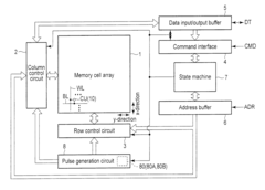
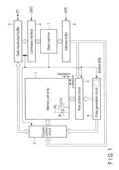
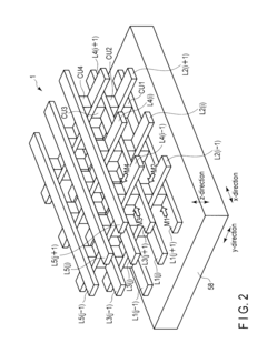
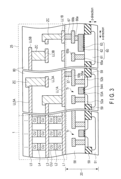
Resistance-change memory and method of operating the same
PatentInactiveUS20120014164A1
Innovation
- The implementation of a resistance-change memory with a pulse generation circuit that generates specific pulses to change the resistance state of the memory element, including a set pulse, reset pulse, read pulse, and dummy pulse, to improve data retention and operational reliability, with a control circuit managing these operations.
Performance Benchmarking of Emerging Memory Technologies
In the landscape of emerging memory technologies, performance benchmarking provides critical insights for evaluating the potential of Resistive RAM (ReRAM) against other contenders. ReRAM demonstrates impressive read/write speeds ranging from 10-100ns, positioning it favorably between DRAM (~10ns) and NAND flash (~100μs). This performance characteristic makes ReRAM particularly suitable for applications requiring moderate speed with non-volatility.
When examining energy efficiency, ReRAM consumes approximately 0.1-1pJ per bit operation, significantly outperforming NAND flash (~10pJ) and approaching the efficiency of STT-MRAM. This low power consumption represents a crucial advantage for mobile and IoT applications where energy constraints are paramount.
Endurance testing reveals ReRAM can typically withstand 10^6-10^9 write cycles, substantially exceeding NAND flash (10^4-10^5 cycles) but falling short of DRAM and SRAM (>10^15 cycles). This positions ReRAM as an excellent candidate for storage-class memory applications requiring moderate write intensity.
Density metrics show ReRAM achieving 4-8F² cell sizes, comparable to NAND flash and superior to SRAM and MRAM technologies. This high-density characteristic enables cost-effective scaling for mass storage applications, though 3D integration remains less mature than in NAND technology.
Retention performance of ReRAM is impressive, with data preservation capabilities of 10+ years at standard operating temperatures, matching or exceeding most competing non-volatile technologies. This long-term stability ensures data integrity without refresh requirements.
Latency analysis demonstrates ReRAM's balanced performance with read latencies of 10-100ns and write latencies of 50-500ns. This positions it between high-speed volatile memories and slower storage technologies, making it suitable for bridging the memory-storage gap.
Scalability assessment indicates ReRAM can be manufactured at advanced nodes (22nm and below) with promising scaling potential to sub-10nm nodes. However, challenges remain in maintaining consistent switching behavior at these dimensions compared to more mature NAND technology.
Multi-level cell capabilities in ReRAM show potential for 2-4 bits per cell, enhancing density but with reliability trade-offs. This capability, while not as developed as in NAND flash (4+ bits/cell), offers a pathway to increased storage density in future implementations.
Manufacturing Scalability and Cost Analysis
Manufacturing scalability represents a critical factor in the commercial viability of emerging memory technologies. Resistive RAM (RRAM) demonstrates significant advantages in this domain compared to other emerging memory technologies. RRAM's relatively simple structure, consisting primarily of a metal-insulator-metal stack, enables integration with standard CMOS processes using existing semiconductor manufacturing equipment. This compatibility significantly reduces the capital expenditure required for production implementation compared to technologies requiring specialized fabrication tools.
When examining manufacturing costs, RRAM benefits from fewer processing steps than competing technologies like MRAM and PCM. MRAM requires precise deposition of multiple magnetic layers with strict thickness control, while PCM demands specialized materials and high-temperature processing. RRAM's simpler structure translates to higher throughput, lower material costs, and reduced manufacturing complexity, contributing to a more favorable cost structure at scale.
The scalability of RRAM extends to its dimensional characteristics. Current research demonstrates RRAM cells scaling below 10nm, with theoretical scaling limits approaching 5nm. This compares favorably to MRAM, which faces challenges scaling below 20nm due to thermal stability issues in smaller magnetic tunnel junctions. PCM similarly encounters difficulties at extreme dimensions due to thermal interference between adjacent cells.
Yield considerations also favor RRAM in large-scale manufacturing scenarios. The relatively straightforward fabrication process results in fewer defect opportunities compared to the complex multi-layer structures of MRAM or the precise crystallization requirements of PCM. Higher yields directly impact per-unit costs, providing RRAM with another economic advantage in high-volume production environments.
From a materials perspective, RRAM primarily utilizes abundant elements like titanium, hafnium, and oxygen, avoiding the supply chain vulnerabilities associated with rare earth elements required for some MRAM implementations. This materials advantage provides greater price stability and reduces geopolitical supply risks in large-scale manufacturing operations.
Cost modeling projections indicate that at mature production volumes, RRAM could achieve bit costs approaching those of NAND flash while delivering superior performance characteristics. However, challenges remain in standardizing RRAM manufacturing processes across the industry, as various material systems and switching mechanisms are still being explored by different manufacturers, potentially fragmenting the ecosystem and delaying economies of scale.
Unlock deeper insights with PatSnap Eureka Quick Research — get a full tech report to explore trends and direct your research. Try now!
Generate Your Research Report Instantly with AI Agent
Supercharge your innovation with PatSnap Eureka AI Agent Platform!