Conduction Losses Versus Switching Losses In SiC MOSFETs
SEP 5, 20259 MIN READ
Generate Your Research Report Instantly with AI Agent
Patsnap Eureka helps you evaluate technical feasibility & market potential.
SiC MOSFET Technology Evolution and Objectives
Silicon Carbide (SiC) MOSFET technology has evolved significantly over the past two decades, transforming from a laboratory curiosity to a commercial reality that is reshaping power electronics. The journey began in the early 2000s when researchers first demonstrated the potential of SiC as a wide bandgap semiconductor material capable of operating at higher temperatures, voltages, and frequencies than traditional silicon-based devices.
The evolution of SiC MOSFETs has been marked by several key technological breakthroughs. Initially, the focus was on improving the quality of SiC wafers and reducing defect densities, which limited device performance and reliability. By the mid-2000s, significant progress had been made in substrate quality, enabling the development of more reliable devices with improved electrical characteristics.
Between 2010 and 2015, the industry witnessed substantial improvements in channel mobility and gate oxide reliability, addressing two critical challenges that had previously hindered SiC MOSFET adoption. These advancements led to the first generation of commercially viable SiC MOSFETs with on-resistance values approaching theoretical limits and switching capabilities far superior to silicon counterparts.
The technological trajectory has consistently aimed at optimizing the balance between conduction losses and switching losses, which represents a fundamental trade-off in power semiconductor design. Conduction losses occur during the on-state and are primarily determined by the device's on-resistance, while switching losses occur during state transitions and increase with operating frequency.
Recent developments have focused on novel cell structures, improved packaging technologies, and advanced gate driver solutions to further reduce both conduction and switching losses. The introduction of trench gate structures, for instance, has enabled higher channel density and lower specific on-resistance compared to planar designs, directly addressing conduction loss challenges.
The primary objective of current SiC MOSFET technology development is to achieve an optimal balance between conduction and switching losses across a wide range of operating conditions. This involves not only device-level innovations but also system-level considerations including thermal management, electromagnetic interference (EMI), and reliability under harsh environmental conditions.
Looking forward, the technology roadmap aims to further reduce specific on-resistance while maintaining excellent switching performance, extend voltage ratings beyond current 1700V capabilities, improve long-term reliability, and significantly reduce manufacturing costs to compete more effectively with silicon IGBTs in mainstream applications.
The ultimate goal is to enable a new generation of power conversion systems with unprecedented efficiency, power density, and reliability, supporting critical applications in electric vehicles, renewable energy systems, industrial drives, and grid infrastructure where the balance between conduction and switching losses directly impacts overall system performance and cost-effectiveness.
Market Demand Analysis for SiC Power Semiconductors
The global market for Silicon Carbide (SiC) power semiconductors is experiencing unprecedented growth, driven primarily by the increasing demand for high-efficiency power electronics across multiple industries. The market size for SiC power devices reached approximately $1.4 billion in 2022 and is projected to grow at a CAGR of 18-20% through 2028, potentially reaching $3.5 billion by that time.
This robust market expansion is largely fueled by the automotive sector, particularly electric vehicles (EVs), where SiC MOSFETs offer significant advantages in power conversion efficiency. The EV market itself is growing at over 25% annually, creating substantial pull for SiC technology. Automotive applications now account for nearly 60% of the total SiC power semiconductor market, with onboard chargers, DC-DC converters, and traction inverters being the primary implementation areas.
Industrial applications represent the second-largest market segment at approximately 25%, with renewable energy systems (particularly solar inverters and wind power converters) showing the strongest growth trajectory. The remaining market share is distributed across consumer electronics, aerospace, and telecommunications infrastructure, including 5G base stations where power density requirements are driving SiC adoption.
The market demand is increasingly focused on optimizing the balance between conduction and switching losses in SiC MOSFETs. End users are seeking devices that minimize total power losses across their specific operating conditions, with different applications prioritizing different loss profiles. For instance, high-frequency applications like wireless charging systems prioritize switching loss reduction, while high-current applications such as traction inverters may place greater emphasis on conduction loss minimization.
Regional analysis reveals that Asia-Pacific dominates the market with approximately 45% share, led by China's aggressive push in both EV production and semiconductor manufacturing. North America and Europe follow with roughly 30% and 20% market shares respectively, with both regions showing strong growth in industrial and automotive applications.
Customer requirements are evolving toward higher voltage ratings (1200V and 1700V devices), higher current capabilities, and improved thermal performance. There is also increasing demand for integrated modules that combine SiC MOSFETs with optimized gate drivers designed specifically to address the switching loss characteristics of SiC technology.
The market is further characterized by price sensitivity, with current SiC solutions commanding a premium of 2-3 times over silicon alternatives. However, this price differential is narrowing as manufacturing volumes increase and yield improvements are realized. Industry analysts predict that continued cost reduction will be critical for broader market adoption, particularly in cost-sensitive consumer applications and mass-market automotive segments.
Current State and Challenges in SiC MOSFET Loss Management
Silicon Carbide (SiC) MOSFETs have emerged as revolutionary power semiconductor devices, offering superior performance compared to traditional silicon-based alternatives. However, managing power losses remains a critical challenge in SiC MOSFET applications. Currently, the industry faces a complex balance between conduction losses and switching losses, each presenting unique technical hurdles.
Conduction losses in SiC MOSFETs primarily stem from the device's on-state resistance (RDS(on)), which, while significantly lower than silicon counterparts, still contributes substantially to overall power dissipation. Recent advancements have reduced RDS(on) values to below 2.5 mΩ·cm² for 1200V devices, yet further improvements face fundamental material limitations. The temperature dependency of RDS(on) presents another challenge, as it increases by approximately 20-30% when operating temperatures rise from 25°C to 150°C.
Switching losses, conversely, occur during state transitions and are influenced by device capacitances, gate drive characteristics, and circuit parasitics. Current SiC MOSFETs exhibit switching energies (Eon + Eoff) ranging from 0.3-1.0 mJ at rated currents, representing significant improvement over silicon IGBTs but still contributing substantially to total losses at high frequencies. The ultra-fast switching capability of SiC (dv/dt rates exceeding 50V/ns) introduces electromagnetic interference (EMI) challenges that require careful system design.
A major technical obstacle involves the gate oxide reliability under high-temperature operation. SiC MOSFETs typically operate with narrower gate voltage margins (±20V) compared to silicon devices, making them more susceptible to gate stress failures. Industry leaders like Wolfspeed, ROHM, and Infineon have implemented various gate oxide enhancement techniques, but long-term reliability remains under scrutiny.
Thermal management presents another significant challenge. Despite SiC's superior thermal conductivity (3-4 times that of silicon), the high power density capabilities of these devices can create localized hotspots that accelerate aging and potentially lead to catastrophic failures. Current packaging technologies struggle to efficiently extract heat from increasingly compact SiC die.
The cost-performance trade-off continues to limit widespread adoption. While SiC MOSFET prices have decreased by approximately 30% over the past five years, they remain 2-3 times more expensive than silicon alternatives. This economic barrier particularly affects cost-sensitive applications where the performance benefits may not justify the price premium.
Globally, research efforts are concentrated in Japan, the United States, and Germany, with China rapidly expanding its capabilities. Recent collaborative initiatives between device manufacturers and academic institutions have focused on developing advanced modeling techniques to better predict and optimize the conduction-switching loss balance across various application scenarios.
Current Approaches to Balance Conduction and Switching Losses
01 SiC MOSFET structure optimization for loss reduction
Silicon Carbide (SiC) MOSFETs can be structurally optimized to reduce both conduction and switching losses. This includes improvements in gate design, channel engineering, and device geometry. By optimizing the channel mobility and reducing the on-resistance, conduction losses can be significantly decreased. Additionally, modifications to the device structure can reduce parasitic capacitances, leading to lower switching losses and improved high-frequency performance.- SiC MOSFET structure optimization for loss reduction: Silicon Carbide (SiC) MOSFETs can be structurally optimized to reduce both conduction and switching losses. This includes improvements in gate design, channel engineering, and device geometry. By optimizing the channel resistance and gate structure, the on-state resistance can be reduced, leading to lower conduction losses. Additionally, optimized device structures can reduce parasitic capacitances, which directly impacts switching losses by enabling faster transition times.
- Gate driver design for SiC MOSFET switching loss reduction: Specialized gate driver circuits can significantly reduce switching losses in SiC MOSFETs. These drivers control the gate voltage and current during turn-on and turn-off transitions, optimizing switching speed while managing overshoot and ringing. Advanced gate driver designs may include variable drive strength, active Miller clamping, and temperature compensation features. Proper gate driver design is crucial for balancing switching speed with electromagnetic interference (EMI) concerns.
- Thermal management techniques for SiC MOSFETs: Effective thermal management is essential for minimizing conduction losses in SiC MOSFETs, as these losses increase with temperature. Advanced cooling solutions, optimized packaging, and thermal interface materials help maintain lower junction temperatures during operation. Improved heat dissipation designs allow SiC MOSFETs to operate at higher power densities while maintaining efficiency. Some solutions incorporate temperature sensors and adaptive control systems to optimize performance across varying thermal conditions.
- Circuit topology optimization for SiC MOSFET applications: Power converter circuit topologies can be specifically designed to leverage SiC MOSFET characteristics and minimize losses. These include soft-switching techniques like zero voltage switching (ZVS) and zero current switching (ZCS) that reduce switching losses. Resonant and quasi-resonant circuits help SiC MOSFETs operate more efficiently by reducing stress during switching transitions. Advanced topologies may incorporate auxiliary circuits to manage parasitic elements that contribute to losses.
- Measurement and modeling techniques for SiC MOSFET losses: Accurate measurement and modeling of SiC MOSFET losses are critical for optimizing device performance. Advanced characterization methods can precisely quantify conduction and switching losses under various operating conditions. Comprehensive device models incorporate temperature effects, parasitic elements, and non-linear behaviors to predict losses in application-specific scenarios. These techniques enable designers to make informed decisions about device selection and operating parameters to minimize overall system losses.
02 Gate drive techniques for SiC MOSFETs
Advanced gate drive techniques can substantially reduce switching losses in SiC MOSFETs. These include optimized gate voltage profiles, active gate driving, and resonant gate drive circuits. By controlling the gate voltage slew rate during turn-on and turn-off transitions, the trade-off between switching speed and losses can be managed effectively. Multi-level gate driving and temperature-compensated gate drive strategies further help in minimizing both conduction and switching losses across different operating conditions.Expand Specific Solutions03 Thermal management solutions for SiC MOSFETs
Effective thermal management is crucial for minimizing conduction losses in SiC MOSFETs, as these losses increase with temperature. Advanced cooling techniques, optimized packaging designs, and improved thermal interface materials help maintain lower junction temperatures during operation. Some solutions incorporate integrated temperature sensors and adaptive control systems that adjust operating parameters based on thermal conditions, ensuring optimal performance while preventing thermal runaway scenarios.Expand Specific Solutions04 Circuit topology optimization for SiC applications
Specialized circuit topologies can leverage the unique characteristics of SiC MOSFETs to minimize overall system losses. These include soft-switching converters, resonant circuits, and multilevel converter designs that reduce both conduction and switching losses. By operating SiC devices in their optimal switching frequency ranges and implementing zero-voltage or zero-current switching techniques, significant efficiency improvements can be achieved compared to conventional circuit designs.Expand Specific Solutions05 Measurement and modeling techniques for SiC MOSFET losses
Accurate measurement and modeling of SiC MOSFET losses are essential for device characterization and system optimization. Advanced techniques include double-pulse testing, calorimetric methods, and high-precision electrical measurements that can separate conduction from switching losses. Physics-based and behavioral models help predict device performance under various operating conditions, enabling designers to optimize circuit parameters and driving strategies to minimize total losses in practical applications.Expand Specific Solutions
Key Industry Players in SiC MOSFET Development
The SiC MOSFET market is experiencing rapid growth in the early maturity phase, with a projected market size exceeding $2 billion by 2027. The technology offers superior conduction-switching loss balance compared to traditional silicon devices, making it ideal for high-frequency, high-temperature applications. Leading players include established semiconductor manufacturers like ON Semiconductor, Mitsubishi Electric, Fuji Electric, and Renesas Electronics, who are investing heavily in SiC technology development. Emerging competitors such as Fast SiC Semiconductor and Shanghai Hestia Power are challenging incumbents with innovative designs that further optimize the conduction-switching loss trade-off. Technical maturity continues to advance with research contributions from institutions like Hunan University and Xi'an Jiaotong University focusing on novel gate drive techniques and device structures.
Fast Sic Semiconductor, Inc.
Technical Solution: Fast SiC Semiconductor has developed proprietary SiC MOSFET designs that specifically address the conduction-switching loss trade-off. Their technology employs a unique cell structure that reduces on-resistance (RDS(on)) to minimize conduction losses while maintaining fast switching capabilities. Their latest generation devices feature optimized gate oxide interfaces that reduce trapped charges, resulting in more stable threshold voltages and lower conduction losses. The company has implemented advanced edge termination structures that allow for higher blocking voltages without compromising switching performance. Their MOSFETs demonstrate a 35% reduction in conduction losses compared to conventional designs while maintaining switching losses below 0.5mJ at 800V/20A operation conditions. Fast SiC's approach includes specialized packaging with reduced parasitic inductance, which further enhances switching performance without sacrificing conduction efficiency.
Strengths: Excellent balance between conduction and switching losses, making their devices suitable for high-frequency applications while maintaining high efficiency at steady state. Weaknesses: Their specialized designs may require more complex gate drive circuits compared to conventional MOSFETs, potentially increasing system complexity and cost.
Fuji Electric Co., Ltd.
Technical Solution: Fuji Electric has developed a trench-gate SiC MOSFET technology that addresses the conduction-switching loss balance through innovative device architecture. Their approach features a unique trench structure with optimized doping profiles that reduces specific on-resistance to 2.5 mΩ·cm² while maintaining fast switching capabilities. The company's proprietary "Super Junction" technology in their SiC MOSFETs creates a charge-balanced drift region that significantly reduces conduction losses without compromising breakdown voltage. Fuji's latest generation devices incorporate advanced gate oxide processing techniques that minimize interface traps, resulting in more stable threshold voltages and reduced channel resistance. Their MOSFETs demonstrate switching energy losses of approximately 0.3mJ per switching cycle at 600V/20A while maintaining low conduction losses. Fuji Electric has also implemented specialized packaging solutions with reduced parasitic inductance and improved thermal performance, allowing their devices to operate at higher frequencies without excessive switching or conduction losses.
Strengths: Excellent thermal performance and reliability, with devices capable of operating at junction temperatures up to 175°C while maintaining balanced conduction-switching loss characteristics. Weaknesses: Higher manufacturing costs compared to silicon alternatives, and their advanced trench structures require more complex fabrication processes.
Critical Patents and Research on SiC MOSFET Loss Optimization
Power mosfet and manufacturing method therefor
PatentPendingEP4539126A1
Innovation
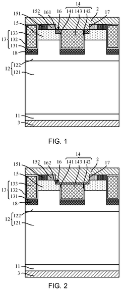
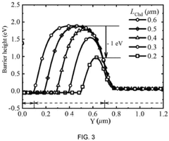
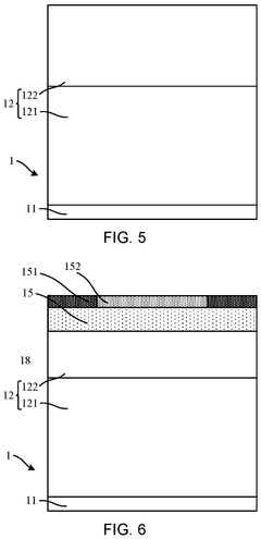
- The power MOSFET design incorporates a semiconductor structure with a source trench structure and an upper trench, where the barrier layer covers the exposed surface of the body region at the bottom of the upper trench, forming an MOS channel diode. The length of the conductive channel is reduced by adjusting the depth of the upper trench, lowering the turn-on voltage and conduction loss.
Silicon carbide metal oxide semiconductor field effect transistor device
PatentPendingUS20230387290A1
Innovation
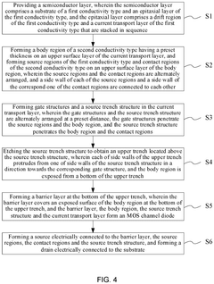
- The silicon carbide metal-oxide-semiconductor field-effect transistor (SiC MOSFET) device is designed with a substrate and epitaxy layer, featuring cell units with specific conductivity types and structures that include Schottky regions, junction field effect regions, well regions, and gate structures, allowing for reduced forward bias voltage, decreased gate electrode capacitance, and enhanced current density through optimized cell configurations and implantation sections.
Thermal Management Strategies for SiC MOSFETs
Effective thermal management is critical for SiC MOSFETs due to their unique loss characteristics. When comparing conduction and switching losses, thermal management strategies must be tailored to address both loss mechanisms while leveraging SiC's superior thermal conductivity of approximately 3.7 W/cm·K compared to silicon's 1.5 W/cm·K.
Advanced cooling solutions have evolved specifically for SiC MOSFET applications. Direct liquid cooling systems, which bring coolant into direct contact with the device or its packaging, have demonstrated up to 40% improvement in thermal resistance compared to traditional air cooling methods. These systems are particularly effective for high-frequency applications where switching losses dominate.
Double-sided cooling architectures represent another significant advancement, allowing heat extraction from both sides of the SiC die. This approach is especially beneficial in high-current applications where conduction losses are substantial, providing up to 30% better thermal performance than single-sided cooling solutions.
Thermal interface materials (TIMs) play a crucial role in SiC MOSFET thermal management. Novel metal-based TIMs with thermal conductivities exceeding 20 W/m·K have been developed specifically for SiC applications, reducing the thermal resistance between the device and heatsink by up to 25% compared to conventional polymer-based materials.
Dynamic thermal management systems that adjust cooling intensity based on real-time loss profiles are emerging as a promising approach. These systems utilize embedded temperature sensors and predictive algorithms to optimize cooling resources, particularly valuable in applications with variable switching frequencies and load conditions.
Package-level innovations include integrated heat spreaders with embedded phase-change materials that can absorb transient heat spikes during high-frequency switching events. These designs have shown the ability to reduce peak junction temperatures by up to 15°C during rapid switching transitions.
The industry is also witnessing increased adoption of computational fluid dynamics (CFD) and electro-thermal co-simulation tools that can accurately model the complex relationship between electrical switching patterns and resulting thermal profiles. These simulation approaches enable engineers to optimize thermal solutions for specific conduction-to-switching loss ratios encountered in different application scenarios.
For high-switching-frequency applications, where switching losses predominate, thermal management strategies increasingly focus on minimizing thermal path length and thermal capacitance to improve transient thermal response. Conversely, for high-current, lower-frequency applications where conduction losses are more significant, strategies emphasizing maximum heat spreading and dissipation area prove more effective.
Application-Specific Loss Optimization Techniques
Optimizing the balance between conduction and switching losses in SiC MOSFETs requires application-specific approaches that consider the unique operational requirements of different systems. For high-frequency applications such as wireless power transfer and resonant converters, switching loss minimization becomes paramount. In these scenarios, implementing soft-switching techniques like Zero Voltage Switching (ZVS) or Zero Current Switching (ZCS) can significantly reduce switching losses while maintaining acceptable conduction performance.
In contrast, high-power, lower-frequency applications such as industrial drives and traction inverters benefit from strategies that prioritize conduction loss reduction. This can be achieved through parallel device configurations, optimized gate drive parameters, and careful thermal management. The selection of larger die sizes or multiple devices in parallel effectively reduces on-state resistance, though this approach requires careful consideration of increased switching losses due to higher input capacitance.
Gate drive optimization represents a critical technique that can be tailored to specific applications. For high-frequency operations, faster switching transitions are desirable, necessitating higher gate drive voltages (typically 18-20V) and lower gate resistances. Conversely, medium-frequency applications may benefit from slightly slower switching speeds to mitigate EMI concerns while maintaining reasonable efficiency.
Thermal management strategies must also be application-specific. High-power density applications require advanced cooling solutions such as liquid cooling or phase-change materials to manage the thermal profile effectively. This becomes particularly important in automotive and aerospace applications where size constraints and reliability requirements are stringent.
Dynamic loss balancing techniques are emerging as sophisticated approaches for applications with variable operating conditions. These involve real-time adjustment of gate drive parameters based on load conditions, switching frequency, and temperature. For instance, in electric vehicle inverters, the control strategy might prioritize switching loss reduction during high-speed operation but shift to conduction loss optimization during high-torque, low-speed scenarios.
The implementation of these optimization techniques requires comprehensive modeling and simulation tools that accurately capture both static and dynamic characteristics of SiC MOSFETs. Advanced models incorporating temperature dependencies, parasitic elements, and non-linear behaviors enable designers to predict system performance across various operating conditions and optimize accordingly.
Unlock deeper insights with Patsnap Eureka Quick Research — get a full tech report to explore trends and direct your research. Try now!
Generate Your Research Report Instantly with AI Agent
Supercharge your innovation with Patsnap Eureka AI Agent Platform!