Cost Trends And Market Adoption Of SiC MOSFET Technology
SEP 5, 20259 MIN READ
Generate Your Research Report Instantly with AI Agent
Patsnap Eureka helps you evaluate technical feasibility & market potential.
SiC MOSFET Evolution and Objectives
Silicon Carbide (SiC) MOSFET technology has evolved significantly since its initial development in the early 1990s. The journey began with rudimentary devices exhibiting high on-resistance and limited reliability, primarily confined to laboratory research. By the early 2000s, commercial viability started to emerge as manufacturers like Cree (now Wolfspeed) and Rohm introduced the first generation of SiC MOSFETs with improved performance characteristics.
The evolution accelerated around 2010-2015 when second-generation devices achieved substantial reductions in on-resistance and switching losses, enabling practical applications in power electronics. This period marked the transition from experimental technology to commercially viable solutions, though still at premium price points that limited widespread adoption.
From 2015 onwards, the technology entered a rapid development phase characterized by manufacturing scale improvements, design optimizations, and enhanced reliability. The introduction of planar and trench MOSFET structures represented significant architectural advancements, offering better performance-to-cost ratios and addressing earlier reliability concerns related to gate oxide stability.
Current generation SiC MOSFETs (2020 onwards) demonstrate remarkable characteristics: breakdown voltages exceeding 1700V, specific on-resistances below 3 mΩ·cm², and switching frequencies up to 100 kHz in practical applications. These improvements have positioned SiC as a viable alternative to silicon IGBTs in numerous high-power applications.
The technology evolution trajectory suggests several clear objectives for future development. Primary among these is cost reduction through improved manufacturing yields, larger wafer sizes (transitioning from 6-inch to 8-inch), and optimized device designs. Current SiC MOSFETs typically command a 3-5x price premium over silicon alternatives, representing a significant barrier to broader market penetration.
Another critical objective is reliability enhancement, particularly addressing concerns about gate oxide stability under high-temperature operation and long-term drift characteristics. Manufacturers are targeting automotive-grade qualification standards to enable wider adoption in electric vehicle powertrains, requiring demonstrated reliability for 15+ year operational lifespans.
Performance objectives focus on further reducing specific on-resistance, improving high-temperature operation capabilities beyond 200°C, and enhancing switching performance to enable higher frequency operation with minimal losses. These improvements would unlock new application domains currently inaccessible to silicon-based devices.
The industry is also pursuing packaging innovations to fully leverage SiC's thermal and electrical characteristics, with objectives to develop specialized packages that can withstand higher operating temperatures while minimizing parasitic inductances that limit switching performance.
SiC MOSFET Market Demand Analysis
The global SiC MOSFET market has experienced substantial growth in recent years, driven primarily by increasing demand for high-efficiency power electronics across multiple industries. Market research indicates that the SiC MOSFET market was valued at approximately $600 million in 2021 and is projected to reach $2.5 billion by 2027, representing a compound annual growth rate (CAGR) of around 27% during this forecast period.
The automotive sector has emerged as the dominant application area for SiC MOSFETs, accounting for nearly 60% of the total market demand. This is largely attributed to the rapid expansion of electric vehicle (EV) production worldwide. SiC MOSFETs offer significant advantages in EV applications, including reduced power losses, higher temperature operation, and smaller form factors compared to traditional silicon-based devices. These benefits translate directly into extended driving range, faster charging capabilities, and more compact power electronics systems.
Industrial applications represent the second-largest market segment, with particular growth in renewable energy systems, industrial motor drives, and power supplies. The superior switching characteristics and efficiency of SiC MOSFETs make them increasingly attractive for solar inverters and wind power converters, where even marginal efficiency improvements can yield substantial energy savings over system lifetimes.
Regional analysis reveals that Asia-Pacific currently dominates the SiC MOSFET market with approximately 45% market share, followed by North America and Europe. China, in particular, has demonstrated aggressive adoption rates, supported by government initiatives promoting electric vehicles and renewable energy infrastructure.
Market penetration analysis indicates that while SiC MOSFETs have achieved significant adoption in premium EV models and high-end industrial applications, broader market penetration remains constrained by cost factors. The average price premium for SiC MOSFETs compared to silicon alternatives has decreased from approximately 10x to 3-4x over the past five years, yet this differential continues to limit adoption in cost-sensitive applications.
Consumer demand patterns show increasing preference for products offering improved energy efficiency, which indirectly drives SiC MOSFET adoption. This trend is particularly evident in regions with high electricity costs or stringent energy efficiency regulations. Market surveys indicate that 78% of industrial customers consider power efficiency as a "very important" factor in their purchasing decisions for power electronics systems.
Future market growth is expected to be fueled by expanding applications in 5G infrastructure, data centers, and aerospace systems, where the performance advantages of SiC technology can justify the higher component costs. Additionally, the ongoing electrification trend across multiple industries suggests sustained long-term demand growth for SiC MOSFETs.
SiC MOSFET Development Status and Barriers
Silicon Carbide (SiC) MOSFET technology has made significant strides globally, with major advancements in both material quality and device performance. Currently, commercial SiC MOSFETs offer blocking voltages ranging from 650V to 1700V, with research prototypes demonstrating capabilities up to 15kV. The technology has matured considerably over the past decade, transitioning from laboratory curiosity to commercial viability across multiple applications.
Despite this progress, several critical technical challenges persist. Channel mobility remains substantially lower than theoretical limits due to interface traps and surface roughness at the SiC/SiO2 interface. This results in higher on-resistance compared to silicon counterparts of similar voltage ratings, limiting efficiency gains in certain applications. Oxide reliability also presents significant concerns, with threshold voltage instability under high-temperature and high-field conditions affecting long-term performance.
Manufacturing yield represents another substantial barrier. SiC wafers exhibit higher defect densities than silicon, including micropipes, dislocations, and basal plane defects. These defects can lead to premature device failure and contribute to the higher cost structure of SiC devices. Current 6-inch SiC wafer production shows defect densities approximately 10-100 times higher than comparable silicon wafers.
The geographical distribution of SiC technology development shows concentration in three main regions. North America leads in innovation with companies like Wolfspeed, ON Semiconductor, and academic centers at Purdue and Ohio State University. Europe maintains strong positions through STMicroelectronics and Infineon, while Asia has rapidly expanded capabilities with ROHM, Mitsubishi Electric, and aggressive investment from Chinese entities like CRRC and BYD Semiconductor.
Cost remains perhaps the most significant barrier to widespread adoption. Current SiC MOSFETs typically command a 3-5x price premium over silicon alternatives, though this gap has narrowed from the 8-10x differential observed five years ago. The cost structure is heavily influenced by substrate expenses (approximately 40% of total cost), specialized epitaxial growth processes (25%), and lower yields in device fabrication (contributing to the remaining 35%).
Packaging technology presents additional challenges unique to SiC devices. The high-temperature capabilities of SiC (theoretically operational up to 600°C) cannot be fully utilized due to limitations in conventional packaging materials and interconnect technologies, which typically degrade above 175-200°C. This creates a technological bottleneck where the semiconductor itself outperforms its packaging environment.
Current SiC MOSFET Cost Reduction Strategies
01 SiC MOSFET Manufacturing Cost Reduction Strategies
Various strategies are being developed to reduce the manufacturing costs of Silicon Carbide (SiC) MOSFETs. These include improved wafer processing techniques, optimization of epitaxial growth processes, and innovative device structures that maximize yield. Cost reduction is critical for wider market adoption, as traditional silicon-based devices currently maintain a significant cost advantage. Advanced manufacturing methods are helping to close this gap by increasing throughput and reducing defect densities in SiC substrates.- Manufacturing cost reduction strategies for SiC MOSFETs: Various manufacturing techniques and process optimizations have been developed to reduce the production costs of Silicon Carbide (SiC) MOSFETs. These include improved substrate preparation methods, enhanced epitaxial growth processes, and more efficient device fabrication techniques. By implementing these cost reduction strategies, manufacturers can lower the overall production expenses, making SiC MOSFETs more competitive with traditional silicon-based devices while maintaining their superior performance characteristics.
- Market adoption trends and forecasting for SiC power devices: The adoption of SiC MOSFETs in various industries shows significant growth patterns, with particular penetration in electric vehicles, renewable energy systems, and industrial power supplies. Market forecasting models indicate accelerating adoption rates as production scales up and costs decrease. Analysis of market trends reveals key adoption drivers including improved efficiency, higher temperature operation, and faster switching capabilities compared to silicon alternatives. These advantages are increasingly outweighing the higher initial costs as the technology matures.
- Economic analysis of SiC MOSFET implementation in power systems: Economic analyses demonstrate the total cost of ownership benefits when implementing SiC MOSFETs in power conversion systems. While initial component costs remain higher than silicon alternatives, the economic advantages come from system-level benefits including reduced cooling requirements, smaller passive components, higher efficiency, and extended lifetime. These factors contribute to lower operational costs and better return on investment over the product lifecycle, particularly in high-power applications where efficiency improvements translate to significant energy savings.
- Supply chain developments and material cost factors: The SiC MOSFET supply chain has evolved significantly with increased substrate production capacity and more suppliers entering the market. Material costs, particularly high-quality SiC wafers, remain a significant factor in overall device pricing. Recent developments include improved wafer manufacturing techniques, larger diameter substrates, and enhanced material quality control processes. These advancements are gradually reducing material costs while improving yield rates, contributing to the overall downward trend in SiC MOSFET pricing.
- Technological innovations driving cost-performance improvements: Ongoing technological innovations are continuously improving the cost-performance ratio of SiC MOSFETs. These include novel device structures, enhanced gate oxide reliability, improved channel mobility, and advanced packaging solutions. Additionally, innovations in testing methodologies and quality control processes are reducing defect rates and improving manufacturing yields. These technological advancements collectively contribute to better device performance while simultaneously reducing production costs, accelerating market adoption across various power electronics applications.
02 Market Adoption Trends and Economic Analysis
The adoption of SiC MOSFET technology is accelerating in high-power applications where efficiency benefits outweigh cost premiums. Market analysis shows increasing penetration in electric vehicles, renewable energy systems, and industrial power supplies. Economic models predict that as production volumes increase and manufacturing processes mature, the cost differential between SiC and silicon devices will continue to narrow. This trend is supported by government initiatives and industry investments aimed at promoting energy-efficient semiconductor technologies.Expand Specific Solutions03 Technical Advancements Impacting Cost-Performance Ratio
Recent technical innovations are improving the cost-performance ratio of SiC MOSFETs. These include enhanced gate oxide reliability, reduced on-resistance, higher current density designs, and improved thermal management solutions. Such advancements allow manufacturers to offer devices with better performance characteristics while gradually reducing costs. Additionally, packaging innovations are helping to maximize the inherent benefits of SiC technology while minimizing overall system costs, making the technology more attractive for mainstream applications.Expand Specific Solutions04 Supply Chain Development and Material Cost Trends
The SiC MOSFET supply chain is evolving rapidly, with increased investment in substrate production, epitaxial growth capabilities, and specialized fabrication equipment. Material costs, particularly for high-quality SiC wafers, remain a significant factor in overall device pricing. However, trends indicate gradual reduction in material costs as suppliers expand capacity and improve production yields. The development of larger diameter wafers and more efficient material utilization techniques are contributing to more favorable cost structures across the industry.Expand Specific Solutions05 Competitive Landscape and Future Market Projections
The competitive landscape for SiC MOSFET technology is intensifying as more semiconductor manufacturers enter the market. This competition is driving both innovation and price reductions. Market projections indicate continued strong growth, particularly in automotive and industrial sectors, with compound annual growth rates exceeding those of conventional power semiconductors. Future cost trends are expected to follow learning curve models typical of semiconductor technologies, with each doubling of cumulative production volume resulting in predictable cost reductions.Expand Specific Solutions
Key SiC MOSFET Manufacturers and Competitors
The SiC MOSFET technology market is currently in a growth phase, with global adoption accelerating as the technology matures from early commercialization to mainstream implementation. Market size is expanding rapidly, projected to reach significant valuation as electric vehicles, renewable energy systems, and industrial applications increasingly adopt SiC solutions for their superior efficiency and thermal performance. From a technical maturity perspective, companies like Huawei, Mitsubishi Electric, and NXP Semiconductors are leading commercial deployment, while emerging players such as Yangzhou Yangjie Electronic Technology and Shanghai Lanxin Semiconductor are advancing domestic capabilities. Chinese institutions including Xidian University and UESTC are collaborating with State Grid and industrial partners to overcome remaining challenges in reliability and cost reduction, gradually narrowing the gap with international market leaders.
Hitachi Energy Ltd.
Technical Solution: Hitachi Energy has pioneered SiC MOSFET implementation in high-voltage power conversion systems, particularly for grid applications. Their technology features a proprietary planar MOSFET structure with optimized cell geometry that achieves switching frequencies up to 100 kHz while maintaining efficiency above 98%. Hitachi's SiC modules incorporate advanced direct liquid cooling technology that enables power density improvements of approximately 40% compared to conventional IGBT solutions. Their devices feature specially designed gate drivers with active Miller clamp functionality to prevent parasitic turn-on in high-speed switching applications. Hitachi Energy has developed a comprehensive reliability testing protocol specifically for SiC devices that includes power cycling tests exceeding 100,000 cycles at junction temperatures up to 175°C. Their cost reduction roadmap includes the development of larger wafer processing capabilities (moving from 6-inch to 8-inch wafers) and improved epitaxial growth processes that reduce defect densities by approximately 35%, directly impacting yield and cost structure.
Strengths: Extensive experience in high-power applications; strong system-level integration expertise; established global manufacturing and distribution network. Weaknesses: Higher initial cost compared to silicon alternatives; primarily focused on high-power applications rather than consumer electronics, limiting market breadth.
NXP Semiconductors (Thailand) Co., Ltd.
Technical Solution: NXP has developed a comprehensive SiC MOSFET portfolio targeting automotive and industrial applications with voltage ratings from 650V to 1200V. Their technology features a unique double-trench structure that optimizes both channel resistance and JFET region resistance, achieving specific on-resistance below 3.0 mΩ·cm² for 1200V devices. NXP's SiC MOSFETs incorporate advanced sintered silver die-attach technology that improves thermal cycling reliability by 3-5 times compared to conventional soldering methods. Their devices feature integrated temperature and current sensing capabilities that enable real-time condition monitoring and enhanced protection functions. NXP has implemented a sophisticated screening and qualification process that exceeds AEC-Q101 requirements, with extended high-temperature reverse bias testing at 175°C for 1000 hours. Their cost optimization strategy includes partnerships with multiple substrate suppliers and the development of optimized epitaxial growth processes that reduce material consumption while maintaining performance specifications.
Strengths: Strong automotive qualification expertise; established supply chain relationships; comprehensive device and application support ecosystem. Weaknesses: Later market entry compared to some competitors; higher production costs due to rigorous automotive qualification requirements.
Critical SiC MOSFET Patents and Innovations
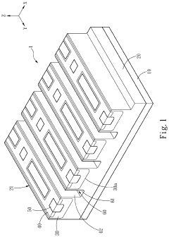
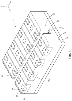
Silicon carbide semiconductor device
PatentPendingUS20240136436A1
Innovation
- A silicon carbide semiconductor device with a hybrid gate structure, featuring a trench structure that reduces JFET resistance and parasitic gate-to-drain capacitance, and increases channel width density, comprising a SiC substrate, drift layer, doped regions, and a gate electrode with a trench gate configuration that forms accumulation layers for low resistance current paths.
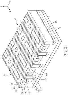
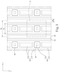
Silicon carbide metal oxide semiconductor field effect transistor and manufacturing method of silicon carbide metal oxide semiconductor field effect transistor
PatentPendingUS20230378341A1
Innovation
- The design incorporates alternating cells with specific well regions, source regions, and contact layers, including ohmic and Schottky contacts, to reduce channel density, enhance short-circuit tolerance, and minimize reverse leakage current and forward voltage drop, while maintaining the transistor's size and functionality.
Supply Chain Resilience for SiC MOSFET Production
The resilience of the SiC MOSFET supply chain has become increasingly critical as market adoption accelerates across automotive, industrial, and renewable energy sectors. Current supply chain structures reveal significant geographical concentration, with key raw material suppliers predominantly located in China, Japan, and the United States. This concentration creates inherent vulnerabilities, as evidenced by the disruptions experienced during the COVID-19 pandemic when SiC wafer production faced substantial delays.
Material sourcing represents a primary challenge, particularly regarding high-purity silicon carbide substrates. The limited number of qualified suppliers capable of meeting the stringent quality requirements for power electronics applications creates potential bottlenecks. Companies like Wolfspeed, II-VI, and ROHM have established vertical integration strategies to mitigate these risks, controlling multiple stages from substrate production to device fabrication.
Manufacturing capacity constraints present another significant vulnerability. The specialized equipment required for SiC processing differs substantially from traditional silicon manufacturing, necessitating dedicated investment. Recent capacity expansion announcements from major players indicate recognition of this challenge, with over $5 billion in collective investments planned through 2025 to address anticipated demand growth.
Geopolitical factors further complicate supply chain stability. Trade tensions between major economies have prompted reassessment of critical semiconductor supply chains, with SiC technology increasingly viewed as strategically important. This has accelerated regionalization efforts, with the European Union's Chips Act and the U.S. CHIPS Act both specifically targeting power semiconductor production capacity.
Diversification strategies are emerging as essential risk mitigation approaches. Leading automotive OEMs have implemented multi-sourcing policies for SiC components, while establishing longer-term supply agreements with preferred vendors. These agreements often include volume commitments and pricing structures that provide stability for both suppliers and customers.
Quality control across the supply chain remains paramount, as SiC MOSFETs for critical applications like electric vehicles require exceptional reliability. The establishment of standardized qualification procedures and testing protocols has helped address this challenge, though variations between supplier specifications continue to create integration complexities for end-users.
Future supply chain resilience will likely depend on continued investment in alternative manufacturing approaches, including potential new substrate technologies that could reduce dependence on traditional SiC crystal growth methods. Additionally, recycling and circular economy initiatives for SiC materials are gaining attention as sustainability concerns grow, potentially offering another avenue to reduce supply vulnerabilities in the longer term.
Environmental Impact of SiC MOSFET Adoption
The adoption of Silicon Carbide (SiC) MOSFET technology presents significant environmental benefits compared to traditional silicon-based power semiconductors. SiC MOSFETs operate at higher temperatures and switching frequencies while maintaining lower switching losses, resulting in more energy-efficient power conversion systems. This efficiency translates directly into reduced energy consumption across various applications, from electric vehicles to industrial power supplies, contributing to lower greenhouse gas emissions throughout product lifecycles.
In electric vehicle applications, SiC MOSFETs enable more efficient power conversion in onboard chargers and traction inverters, extending driving range by 5-10% with the same battery capacity. This efficiency reduces the overall carbon footprint of electric transportation systems and accelerates the transition away from fossil fuel-powered vehicles.
The manufacturing process of SiC devices does require higher energy inputs compared to silicon alternatives due to the higher temperatures needed for crystal growth and processing. However, lifecycle assessments indicate that this initial environmental cost is typically offset within 1-3 years of operation through improved efficiency. The longer operational lifespan of SiC devices—often exceeding 15 years compared to 8-10 years for silicon alternatives—further enhances their environmental credentials by reducing electronic waste generation.
Water usage represents another important environmental consideration. SiC wafer production consumes approximately 30% more water than traditional silicon wafer manufacturing. Industry leaders are addressing this challenge through closed-loop water recycling systems that have reduced freshwater requirements by up to 40% in newer fabrication facilities.
Raw material sourcing for SiC presents fewer environmental concerns than many other semiconductor materials. Silicon carbide is synthesized from abundant materials (silicon and carbon), avoiding the geopolitical and environmental issues associated with rare earth elements used in some alternative technologies.
End-of-life considerations for SiC devices are increasingly important as adoption grows. While currently representing a small fraction of electronic waste, the industry is developing specialized recycling processes to recover valuable materials from spent SiC components. These processes are estimated to recover up to 85% of materials by weight, significantly reducing landfill impact.
As manufacturing scales increase and production processes mature, the environmental footprint of SiC device production continues to decrease. Recent industry reports indicate a 15% reduction in carbon emissions per unit of manufacturing output over the past five years, with further improvements expected as the technology matures and manufacturing efficiencies increase.
Unlock deeper insights with Patsnap Eureka Quick Research — get a full tech report to explore trends and direct your research. Try now!
Generate Your Research Report Instantly with AI Agent
Supercharge your innovation with Patsnap Eureka AI Agent Platform!