

How Do SiC MOSFETs Enable High-Frequency Power Conversion?
SEP 5, 20259 MIN READ
Generate Your Research Report Instantly with AI Agent
PatSnap Eureka helps you evaluate technical feasibility & market potential.
SiC MOSFET Evolution and Objectives
Silicon Carbide (SiC) MOSFETs represent a revolutionary advancement in power semiconductor technology, emerging as a superior alternative to traditional silicon-based devices. The evolution of SiC MOSFETs began in the early 2000s when researchers first demonstrated their potential for high-temperature, high-frequency operation. Since then, the technology has undergone significant refinement, moving from laboratory curiosities to commercially viable products that are reshaping power electronics.
The fundamental advantage of SiC stems from its wide bandgap properties, which enable devices to operate at higher temperatures, voltages, and switching frequencies compared to silicon counterparts. Early SiC MOSFETs faced challenges related to gate oxide reliability, high channel resistance, and manufacturing consistency. However, continuous innovation has addressed these limitations, leading to devices with increasingly optimized performance characteristics.
From 2010 to 2015, the industry witnessed substantial improvements in SiC MOSFET design, with reduced on-resistance, enhanced thermal performance, and better switching characteristics. The period from 2015 to 2020 marked the transition to volume production, with major power semiconductor manufacturers investing heavily in SiC technology and fabrication capabilities. This era saw the emergence of second-generation devices with significantly improved cost-performance ratios.
Current technological trends point toward further miniaturization, enhanced reliability, and reduced costs through improved manufacturing processes. The integration of advanced packaging technologies has also played a crucial role in maximizing the benefits of SiC MOSFETs, particularly for high-frequency applications where parasitic inductances must be minimized.
The primary objective of SiC MOSFET development is to enable power conversion systems that operate at significantly higher frequencies than traditional silicon-based solutions. Higher switching frequencies directly translate to smaller passive components, increased power density, and improved system efficiency. These benefits are particularly valuable in applications such as electric vehicle chargers, renewable energy inverters, and data center power supplies.
Another key objective is to push the boundaries of power density, allowing for more compact and efficient power electronic systems. This aligns with the broader industry trend toward miniaturization and energy efficiency. Additionally, SiC technology aims to enhance system reliability under extreme operating conditions, including high temperatures and high voltage stress.
Looking forward, the roadmap for SiC MOSFETs includes further improvements in device structure, reduction in specific on-resistance, and enhanced short-circuit capability. Research is also focused on addressing challenges related to long-term reliability, particularly under high-temperature operation and repetitive stress conditions. The ultimate goal is to establish SiC MOSFETs as the standard technology for high-frequency power conversion across multiple industries.
Market Demand for High-Frequency Power Conversion
The global market for high-frequency power conversion technologies has experienced substantial growth in recent years, driven primarily by the increasing demand for energy-efficient power systems across multiple industries. This growth trajectory is particularly evident in sectors such as electric vehicles (EVs), renewable energy systems, data centers, and industrial automation, where power density and efficiency are paramount concerns.
In the electric vehicle market, the push for faster charging capabilities and extended range has created significant demand for high-frequency power conversion solutions. The global EV charging infrastructure market reached $17.8 billion in 2021 and is projected to grow at a CAGR of 30.5% through 2028, with high-frequency converters being a critical component enabling rapid charging technologies.
Renewable energy systems represent another major market driver, as solar inverters and wind power converters increasingly require higher switching frequencies to improve efficiency and reduce size. The global solar inverter market alone was valued at $9.3 billion in 2021 and is expected to reach $22.7 billion by 2030, with high-frequency designs capturing an increasing market share.
Data centers constitute a rapidly expanding market segment for high-frequency power conversion, driven by the exponential growth in cloud computing and digital services. With power consumption becoming a critical operational cost factor, data center operators are actively seeking more efficient power conversion solutions that can operate at higher frequencies to reduce energy losses and physical footprint.
Consumer electronics manufacturers are also driving demand for miniaturized, efficient power adapters and chargers. The trend toward universal charging standards like USB-C Power Delivery has accelerated the adoption of high-frequency GaN and SiC-based solutions that can deliver more power in smaller form factors.
Industrial automation systems increasingly require compact, efficient power conversion for motor drives and control systems. The industrial motor drives market, valued at approximately $13.2 billion in 2021, is projected to grow at 5.8% annually through 2028, with high-frequency drives gaining market share due to their superior efficiency and control capabilities.
Market research indicates that the transition to wide-bandgap semiconductor technologies, particularly SiC MOSFETs, is accelerating across these sectors. The global SiC power semiconductor market was valued at $1.1 billion in 2021 and is projected to reach $6.3 billion by 2028, reflecting the strong market pull for technologies enabling high-frequency power conversion.
Regional analysis shows Asia-Pacific leading the market adoption, particularly in consumer electronics and EV applications, while North America dominates in data center and industrial applications. Europe shows strong growth in renewable energy applications, driven by aggressive carbon reduction targets and green energy initiatives.
SiC MOSFET Technology Status and Barriers
Silicon Carbide (SiC) MOSFETs have emerged as revolutionary components in power electronics, yet their widespread adoption faces several significant barriers. Currently, SiC MOSFET technology has matured considerably with commercial devices available from multiple manufacturers including Wolfspeed, ROHM, Infineon, and STMicroelectronics. These devices typically offer blocking voltages ranging from 650V to 1700V, with some specialized solutions reaching up to 3300V for high-power applications.
The primary technological advantage of SiC MOSFETs lies in their wide bandgap properties, enabling operation at junction temperatures exceeding 200°C compared to silicon's 150°C limit. Additionally, SiC's critical electric field strength is approximately 10 times higher than silicon, allowing for thinner drift regions and significantly reduced on-resistance for equivalent voltage ratings.
Despite these advantages, several critical barriers impede broader SiC MOSFET implementation in high-frequency power conversion applications. Gate oxide reliability remains a fundamental challenge, as the interface between SiC and SiO2 contains higher defect densities than silicon-based counterparts. These defects contribute to threshold voltage instability and reduced channel mobility, particularly problematic during high-frequency switching operations.
Manufacturing costs present another substantial barrier. SiC wafer production remains significantly more expensive than silicon, with typical 6-inch SiC wafers costing 5-8 times more than equivalent silicon wafers. The manufacturing process also suffers from lower yields and requires specialized equipment for handling the harder SiC material, further increasing production expenses.
Packaging technology represents a critical limitation for high-frequency applications. Traditional packaging solutions often introduce parasitic inductances that become problematic at frequencies above 100 kHz. While advanced packages like direct-bonded copper (DBC) substrates and silver sintering have improved thermal performance, they add complexity and cost to the final product.
The body diode performance of SiC MOSFETs presents another technical challenge. Unlike silicon devices, SiC MOSFET body diodes exhibit higher forward voltage drops and slower reverse recovery characteristics, potentially limiting efficiency in topologies that rely on body diode conduction during dead time intervals.
From a global perspective, SiC MOSFET technology development shows geographic concentration, with North America, Europe, and Japan leading in intellectual property and manufacturing capabilities. China has recently increased investments significantly, aiming to reduce dependency on foreign suppliers for this strategic technology.
Addressing these barriers requires coordinated efforts across material science, device design, and manufacturing processes. Recent research has focused on alternative gate structures, improved channel mobility through nitridation processes, and novel packaging solutions specifically designed for high-frequency operation. Progress in these areas will be crucial for enabling SiC MOSFETs to fully realize their potential in next-generation high-frequency power conversion systems.
Current SiC MOSFET Design Architectures
01 SiC MOSFET design for high-frequency applications
Silicon Carbide (SiC) MOSFETs can be specifically designed for high-frequency operation by optimizing gate structures, reducing parasitic capacitances, and improving switching characteristics. These design enhancements allow for faster switching speeds, reduced switching losses, and improved thermal performance, making them ideal for high-frequency power conversion applications. The optimized designs enable operation at frequencies significantly higher than traditional silicon-based devices.- SiC MOSFET design for high-frequency applications: Silicon Carbide (SiC) MOSFETs can be specifically designed for high-frequency operation through optimized gate structures, reduced parasitic capacitances, and improved channel mobility. These design enhancements allow for faster switching speeds, reduced switching losses, and better performance at high frequencies. The specialized designs include modifications to the gate oxide interface, channel doping profiles, and device geometry to minimize resistance and capacitance effects that limit high-frequency operation.
- Gate driver circuits for high-frequency SiC MOSFETs: Advanced gate driver circuits are essential for maximizing the high-frequency performance of SiC MOSFETs. These circuits provide optimized gate voltage control, precise timing, and appropriate current levels to enable rapid and efficient switching. Features include isolation techniques, temperature compensation, short-circuit protection, and impedance matching specifically designed for the unique characteristics of SiC devices operating at high frequencies. The gate driver designs help minimize ringing, overshoot, and electromagnetic interference while maintaining switching efficiency.
- Thermal management solutions for high-frequency SiC MOSFETs: Effective thermal management is critical for high-frequency SiC MOSFETs due to increased power density and switching losses at elevated frequencies. Solutions include advanced packaging technologies, integrated cooling systems, optimized heat spreaders, and thermal interface materials with superior conductivity. These thermal management approaches enable SiC MOSFETs to operate reliably at high frequencies by maintaining junction temperatures within safe operating limits, preventing thermal runaway, and extending device lifetime under demanding switching conditions.
- High-frequency power conversion applications using SiC MOSFETs: SiC MOSFETs enable more efficient and compact high-frequency power conversion systems across various applications. These include wireless power transfer, resonant converters, Class D amplifiers, and high-frequency inverters. The superior switching characteristics of SiC MOSFETs allow for operation at frequencies significantly higher than traditional silicon devices, resulting in smaller passive components, increased power density, and improved system efficiency. These applications leverage the fast switching speeds and low losses of SiC technology to achieve performance levels not possible with conventional semiconductor materials.
- Parasitic reduction techniques for high-frequency SiC MOSFETs: Minimizing parasitic inductances and capacitances is essential for optimizing SiC MOSFET performance at high frequencies. Techniques include advanced packaging designs, optimized PCB layouts, integrated bus structures, and novel interconnection methods. These approaches reduce loop inductances, minimize common-source inductance, and optimize gate-drain capacitance effects that would otherwise limit switching speed and increase losses. By addressing these parasitic elements, SiC MOSFETs can achieve their full potential in high-frequency applications with reduced ringing, overshoot, and electromagnetic interference.
02 Gate driver solutions for high-frequency SiC MOSFETs
Specialized gate driver circuits are essential for maximizing the high-frequency performance of SiC MOSFETs. These drivers provide optimized gate voltage profiles, precise timing control, and appropriate current capabilities to ensure fast and efficient switching. Advanced gate driver solutions incorporate features like adjustable slew rates, isolation barriers, and protection mechanisms to handle the unique requirements of SiC devices operating at high frequencies.Expand Specific Solutions03 Thermal management techniques for high-frequency SiC MOSFETs
Effective thermal management is crucial for high-frequency SiC MOSFET operation. Various cooling solutions including advanced heat sinks, liquid cooling systems, and innovative packaging technologies are employed to dissipate heat efficiently. These thermal management techniques enable SiC MOSFETs to operate reliably at high frequencies without performance degradation due to temperature rise, extending device lifetime and maintaining stable electrical characteristics.Expand Specific Solutions04 High-frequency power conversion topologies using SiC MOSFETs
SiC MOSFETs enable the implementation of advanced power conversion topologies optimized for high-frequency operation. These include resonant converters, soft-switching topologies, and multilevel converter architectures that leverage the superior switching characteristics of SiC devices. By operating at higher frequencies, these topologies achieve reduced passive component sizes, improved power density, and enhanced system efficiency compared to traditional silicon-based solutions.Expand Specific Solutions05 Parasitic mitigation techniques for high-frequency SiC MOSFET circuits
Parasitic inductances and capacitances become critical limiting factors in high-frequency SiC MOSFET applications. Various mitigation techniques include optimized PCB layouts, integrated packaging solutions, and specialized interconnection methods to minimize loop inductances and stray capacitances. These techniques reduce ringing, overshoot, and electromagnetic interference, enabling SiC MOSFETs to achieve their full high-frequency performance potential in practical circuit implementations.Expand Specific Solutions
Leading SiC MOSFET Manufacturers and Competitors
The silicon carbide (SiC) MOSFET high-frequency power conversion market is experiencing rapid growth, currently in an early maturity phase with increasing adoption across automotive, renewable energy, and industrial sectors. The global market size is projected to expand significantly, driven by demand for efficient power electronics. Technologically, companies like Wolfspeed, Infineon, ROHM, and Fuji Electric lead with mature commercial offerings, while newer entrants such as Fast SiC Semiconductor and Dongguan TIANYU are advancing capabilities. Academic institutions including Xidian University and University of Electronic Science & Technology of China contribute significant research. The competitive landscape features established semiconductor manufacturers expanding SiC portfolios alongside specialized players focusing exclusively on SiC technology innovation.
Power Integrations, Inc.
Technical Solution: Power Integrations' approach to SiC MOSFET technology focuses on highly integrated solutions that combine SiC switching elements with optimized gate drivers and protection features. Their InnoSwitch™ family incorporating SiC MOSFETs enables switching frequencies up to 140kHz, approximately 3-4 times higher than silicon-based alternatives. The company has developed proprietary gate drive techniques that optimize switching speed while minimizing ringing and EMI issues common in high-frequency SiC implementations. Their devices feature integrated sensing and protection functions specifically calibrated for SiC MOSFET characteristics, including overcurrent, thermal, and short-circuit protection optimized for the faster switching transients of SiC. Power Integrations' solutions achieve power densities exceeding 30W/in³ in AC-DC applications, with efficiency improvements of 3-5% compared to silicon-based designs. Their integrated approach addresses many of the implementation challenges typically associated with discrete SiC MOSFETs in high-frequency applications.
Strengths: Highly integrated solutions simplify design implementation; optimized gate drive specifically designed for SiC characteristics; comprehensive protection features reduce system complexity. Weaknesses: Less flexibility than discrete solutions; limited to specific application segments; higher integration can limit thermal performance in some applications.
ROHM Co., Ltd.
Technical Solution: ROHM's SiC MOSFET technology centers on their proprietary double-trench structure that separates the JFET region from the gate, allowing for optimization of both on-resistance and gate reliability. Their 4th generation SiC MOSFETs achieve switching frequencies up to 100kHz in hard-switching applications and beyond 300kHz in soft-switching topologies. ROHM has developed specialized short-circuit withstand time capabilities exceeding 5μs at rated current and voltage conditions. Their devices feature built-in body diodes with positive temperature coefficient, preventing thermal runaway during high-frequency operation. The company's SiC MOSFETs demonstrate approximately 50% lower switching losses compared to conventional SiC MOSFETs and up to 90% reduction versus silicon IGBTs. ROHM has also pioneered integrated SiC modules combining MOSFETs with optimized gate drivers specifically designed for high-frequency operation, simplifying implementation for power system designers.
Strengths: Proprietary trench structure balancing performance and reliability; comprehensive design support including simulation models and reference designs; strong automotive qualification portfolio. Weaknesses: More limited voltage range offerings compared to some competitors; higher gate threshold voltage variation; thermal performance limitations in some package options.
Key SiC Material Properties and Device Physics
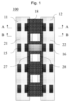
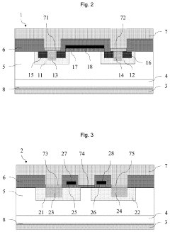
Silicon carbide semiconductor device
PatentPendingUS20240136436A1
Innovation
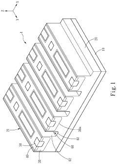
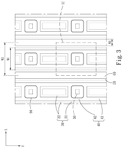
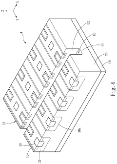
- A silicon carbide semiconductor device with a hybrid gate structure, featuring a trench structure that reduces JFET resistance and parasitic gate-to-drain capacitance, and increases channel width density, comprising a SiC substrate, drift layer, doped regions, and a gate electrode with a trench gate configuration that forms accumulation layers for low resistance current paths.
Silicon carbide metal oxide semiconductor field effect transistor and manufacturing method of silicon carbide metal oxide semiconductor field effect transistor
PatentPendingUS20230378341A1
Innovation
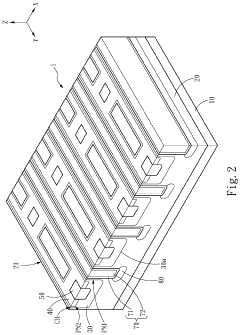
- The design incorporates alternating cells with specific well regions, source regions, and contact layers, including ohmic and Schottky contacts, to reduce channel density, enhance short-circuit tolerance, and minimize reverse leakage current and forward voltage drop, while maintaining the transistor's size and functionality.
Thermal Management Challenges in SiC Applications
Silicon Carbide (SiC) MOSFETs offer significant advantages in high-frequency power conversion applications, but their implementation introduces unique thermal management challenges that must be addressed for reliable operation. The higher switching frequencies enabled by SiC devices result in increased power density, which concentrates heat generation in smaller areas compared to traditional silicon-based solutions.
The thermal conductivity of SiC (approximately 3.7 W/mK) is superior to silicon, allowing for better heat dissipation within the semiconductor itself. However, this advantage is often negated by the thermal bottlenecks that occur at package interfaces and heat spreading structures. The junction-to-case thermal resistance becomes a critical parameter as switching frequencies increase beyond 100 kHz.
Temperature cycling presents another significant challenge in SiC applications. The rapid heating and cooling cycles that occur during high-frequency switching create thermal stress at material interfaces, particularly between the die attach and substrate. This stress can lead to solder fatigue, delamination, and eventual device failure if not properly managed. The coefficient of thermal expansion (CTE) mismatch between SiC and packaging materials exacerbates this issue.
Advanced cooling solutions are becoming essential for SiC MOSFET applications. Traditional air cooling methods often prove insufficient for the power densities achieved in modern SiC converters. Liquid cooling systems, phase-change materials, and direct substrate cooling technologies are increasingly being deployed to maintain junction temperatures within safe operating limits. These cooling technologies must be integrated early in the design process rather than added as afterthoughts.
The dynamic thermal behavior of SiC devices presents unique modeling challenges. Transient thermal impedance becomes increasingly important as pulse widths decrease with higher switching frequencies. Accurate thermal models must account for the non-linear thermal properties of SiC and surrounding materials across a wide temperature range. Computational fluid dynamics (CFD) simulations coupled with electro-thermal models are becoming standard tools for predicting thermal performance.
Gate driver circuits also contribute to thermal management challenges. The higher switching speeds of SiC MOSFETs require gate drivers positioned in close proximity to the power devices, creating additional heat sources in already thermally dense areas. Isolation requirements further complicate thermal design by introducing materials with poor thermal conductivity in critical heat flow paths.
Emerging packaging technologies, such as silver sintering for die attach and embedded cooling channels, are being developed specifically to address SiC thermal challenges. These innovations aim to reduce thermal resistance while improving reliability under the demanding conditions of high-frequency operation.
Reliability and Lifetime Assessment of SiC MOSFETs
The reliability and lifetime assessment of SiC MOSFETs represents a critical consideration for power electronics designers seeking to leverage the high-frequency capabilities of these devices. Unlike traditional silicon-based MOSFETs, SiC devices operate under more extreme conditions, including higher temperatures, voltages, and switching frequencies, which introduces unique reliability challenges.
Accelerated lifetime testing has revealed that SiC MOSFETs demonstrate remarkable robustness under thermal stress, with many commercial devices rated for junction temperatures up to 175°C, significantly higher than silicon counterparts. However, this thermal advantage comes with specific reliability concerns, particularly regarding gate oxide integrity and threshold voltage stability.
The gate oxide in SiC MOSFETs, typically thinner than in silicon devices to achieve comparable threshold voltages, exhibits vulnerability to time-dependent dielectric breakdown (TDDB) under high electric fields. Research indicates that negative bias temperature instability (NBTI) and positive bias temperature instability (PBTI) can cause threshold voltage shifts over time, potentially affecting long-term switching performance in high-frequency applications.
Body diode reliability presents another significant consideration. Unlike silicon MOSFETs, the body diode in SiC devices exhibits higher forward voltage drop and slower reverse recovery characteristics. While this can be advantageous for reducing switching losses, extended operation in third quadrant conduction may lead to increased degradation compared to conventional silicon devices.
Field data from early SiC MOSFET deployments in electric vehicle chargers, solar inverters, and server power supplies indicates promising reliability metrics, with failure rates comparable to or better than silicon alternatives when properly designed into systems. However, these applications typically operate at switching frequencies below 100 kHz, leaving questions about ultra-high-frequency reliability.
Manufacturers have responded to reliability concerns with process improvements, including enhanced gate oxide formation techniques, optimized device structures, and more robust packaging solutions designed specifically for high-temperature, high-frequency operation. These advancements have progressively extended the projected useful life of SiC MOSFETs from early estimates of 5-7 years to current projections exceeding 15 years in many applications.
Reliability modeling for SiC MOSFETs continues to evolve, with physics-of-failure approaches gaining traction over traditional statistical methods. These models incorporate specific degradation mechanisms unique to SiC technology, enabling more accurate lifetime predictions under various operating conditions and switching frequencies.
Unlock deeper insights with PatSnap Eureka Quick Research — get a full tech report to explore trends and direct your research. Try now!
Generate Your Research Report Instantly with AI Agent
Supercharge your innovation with PatSnap Eureka AI Agent Platform!