Reliability Testing And Failure Mechanisms Of SiC MOSFETs
SEP 5, 20259 MIN READ
Generate Your Research Report Instantly with AI Agent
Patsnap Eureka helps you evaluate technical feasibility & market potential.
SiC MOSFET Evolution and Testing Objectives
Silicon Carbide (SiC) MOSFETs have emerged as revolutionary power semiconductor devices, marking a significant advancement beyond traditional silicon-based technologies. The evolution of SiC MOSFETs began in the early 2000s with rudimentary research prototypes, progressing through several generations of commercial devices that have continuously improved in performance, reliability, and cost-effectiveness. This technological trajectory has been driven by the inherent material advantages of SiC, including wider bandgap, higher breakdown field strength, and superior thermal conductivity compared to silicon.
The development timeline reveals distinct evolutionary phases: initial research demonstrations (2000-2005), first commercial offerings with limited performance (2006-2010), second-generation devices with improved gate oxide reliability (2011-2015), and current third-generation devices featuring optimized cell structures and enhanced ruggedness (2016-present). Each generation has addressed specific reliability challenges while expanding the operational envelope of these devices.
Current technological trends indicate continued advancement toward higher voltage ratings (beyond 1700V), lower on-resistance, improved short-circuit capability, and enhanced gate oxide reliability. The industry is witnessing a progressive shift from planar to trench MOSFET structures, enabling higher channel density and reduced specific on-resistance. Concurrently, packaging innovations are evolving to maximize the thermal and switching performance benefits inherent to SiC technology.
The primary objectives of reliability testing for SiC MOSFETs encompass several critical dimensions. First, establishing standardized qualification protocols specifically tailored to SiC devices, as traditional silicon-based testing methodologies may not adequately capture SiC-specific failure mechanisms. Second, determining realistic operational boundaries and safety margins under various stress conditions including temperature, voltage, and switching frequency extremes. Third, identifying and characterizing unique failure modes associated with SiC technology, particularly those related to gate oxide integrity, body diode reliability, and threshold voltage stability.
Additionally, testing objectives include quantifying device lifetime under application-specific mission profiles, evaluating robustness against cosmic radiation (particularly important for high-voltage SiC devices), and developing accelerated testing methodologies that can accurately predict long-term reliability without requiring prohibitively lengthy test durations. The ultimate goal is to establish confidence in SiC MOSFET technology for demanding applications where failure is not an option, such as electric vehicle traction inverters, renewable energy systems, and critical industrial infrastructure.
These testing objectives must balance the need for comprehensive reliability data against time-to-market pressures in a rapidly evolving technological landscape, necessitating innovative approaches to reliability assessment and qualification.
Market Demand Analysis for SiC Power Devices
The global market for Silicon Carbide (SiC) power devices has experienced remarkable growth in recent years, driven primarily by the increasing demand for high-efficiency power electronics across multiple industries. The compound annual growth rate (CAGR) for SiC power devices is projected to exceed 30% through 2026, reflecting the strong market pull for this technology.
Electric vehicle (EV) applications represent the largest and fastest-growing segment for SiC MOSFETs. As automotive manufacturers worldwide accelerate their transition to electric powertrains, the demand for more efficient power conversion systems has intensified. SiC devices enable significant improvements in EV range, charging speeds, and overall system efficiency compared to traditional silicon-based solutions.
Industrial power supplies constitute another major market segment, where SiC MOSFETs offer substantial benefits in terms of energy efficiency and power density. Manufacturing facilities, data centers, and renewable energy systems increasingly adopt SiC technology to reduce operational costs and meet stringent energy efficiency regulations. The industrial sector's demand for SiC devices is expected to grow steadily as more companies prioritize sustainability and energy conservation.
Renewable energy applications, particularly solar inverters and wind power systems, represent a critical growth area for SiC power devices. The superior switching characteristics and thermal performance of SiC MOSFETs enable higher conversion efficiencies in renewable energy systems, directly translating to improved return on investment for clean energy projects. This market segment is expanding rapidly as global renewable energy capacity continues to increase.
Regional analysis reveals that Asia-Pacific currently dominates the SiC power device market, with China, Japan, and South Korea leading in adoption rates. North America and Europe follow closely, with significant growth expected as these regions invest heavily in electrification and renewable energy infrastructure. Government policies promoting energy efficiency and carbon reduction across these regions further accelerate market expansion.
Despite the strong growth trajectory, several factors constrain wider SiC MOSFET adoption. The higher initial cost compared to silicon alternatives remains a significant barrier, particularly for price-sensitive applications. Additionally, concerns about long-term reliability and standardized testing protocols have slowed adoption in mission-critical systems where operational lifetimes of 10-15 years are expected.
Market research indicates that as manufacturing scales increase and reliability concerns are addressed through improved testing methodologies, the cost premium for SiC devices will continue to decrease. This trend, combined with the demonstrable performance advantages, suggests that SiC MOSFETs will progressively displace silicon alternatives in an expanding range of applications, particularly where efficiency, power density, and thermal performance are prioritized.
Current Challenges in SiC MOSFET Reliability
Despite significant advancements in Silicon Carbide (SiC) MOSFET technology, several critical reliability challenges persist that impede its widespread adoption across high-power applications. The primary concern remains the gate oxide reliability, as SiC MOSFETs operate at higher electric fields compared to silicon counterparts, leading to accelerated degradation mechanisms. The interface between SiC and SiO2 exhibits higher defect densities, resulting in threshold voltage instability and reduced channel mobility over time.
Time-dependent dielectric breakdown (TDDB) presents another significant challenge, with SiC MOSFETs showing unique breakdown characteristics that differ from traditional silicon devices. The higher critical field strength in SiC creates more severe conditions at the oxide interface, necessitating specialized testing methodologies to accurately predict lifetime under various operating conditions.
Body diode reliability issues constitute a third major challenge. Unlike silicon MOSFETs, SiC devices exhibit higher forward voltage drops during body diode conduction, leading to increased power losses and potential thermal management issues. Furthermore, the stacking fault expansion phenomenon unique to SiC can cause progressive degradation of the body diode characteristics after repeated stress cycles.
Short-circuit robustness represents a critical reliability concern in practical applications. SiC MOSFETs typically demonstrate shorter short-circuit withstand times compared to silicon IGBTs, primarily due to their smaller die size and higher current densities. This limitation requires careful consideration in designing protection circuits for SiC-based power systems.
Cosmic radiation susceptibility has emerged as an unexpected challenge for high-voltage SiC MOSFETs. The higher critical electric field of SiC allows for thinner drift regions at equivalent voltage ratings, paradoxically making these devices more vulnerable to cosmic ray-induced failures, particularly in aerospace and high-altitude applications.
Package-related reliability issues also persist, as the higher switching speeds and operating temperatures of SiC devices place unprecedented demands on packaging materials and interconnection technologies. Thermal cycling can accelerate bond wire lift-off and solder fatigue, while partial discharge effects become more pronounced at the higher operating voltages typical of SiC applications.
Standardization of reliability testing protocols specifically tailored for SiC MOSFETs remains incomplete. Current testing frameworks, largely derived from silicon device experience, may not adequately capture the unique failure mechanisms of SiC technology, leading to potential underestimation or mischaracterization of long-term reliability risks in field applications.
Established Reliability Testing Methodologies
01 Reliability enhancement through gate oxide improvements
Silicon carbide MOSFETs face reliability challenges due to gate oxide defects. Improving the gate oxide quality through advanced deposition techniques, thermal oxidation processes, and interface treatments can significantly enhance device reliability. These improvements reduce threshold voltage instability, increase breakdown strength, and extend the operational lifetime of SiC MOSFETs under high-temperature and high-electric field conditions.- Reliability enhancement through gate oxide improvements: Silicon carbide MOSFETs reliability can be significantly improved through gate oxide enhancements. Various techniques include optimizing the oxide growth process, implementing nitrogen annealing treatments, and using advanced dielectric materials. These improvements help reduce interface trap density, increase threshold voltage stability, and enhance overall device lifetime under high-temperature and high-field operating conditions.
- Thermal management solutions for SiC MOSFETs: Effective thermal management is crucial for SiC MOSFET reliability. Innovative packaging technologies, advanced heat dissipation structures, and thermally conductive materials are employed to manage the high operating temperatures of SiC devices. These solutions help prevent thermal runaway, reduce thermal resistance, and extend device lifetime under high-power operation conditions.
- Protection circuits and driving strategies: Specialized protection circuits and optimized driving strategies significantly enhance SiC MOSFET reliability. These include short-circuit protection mechanisms, overvoltage protection circuits, and advanced gate driver designs that control switching transients. Proper driving strategies help mitigate stress on the device during switching events, reducing electromagnetic interference and preventing device failure under harsh operating conditions.
- Reliability testing and qualification methodologies: Comprehensive reliability testing and qualification methodologies are essential for evaluating SiC MOSFET performance. These include accelerated lifetime testing, high-temperature gate bias stress tests, short-circuit robustness evaluation, and power cycling tests. Advanced characterization techniques help identify failure mechanisms, predict device lifetime, and establish reliability standards for different application environments.
- Defect reduction and manufacturing process optimization: Improving SiC MOSFET reliability through defect reduction and manufacturing process optimization is critical. This includes substrate quality enhancement, epitaxial growth refinement, and advanced channel formation techniques. Process innovations such as optimized implantation procedures, annealing conditions, and surface treatments help minimize crystal defects, reduce channel resistance, and improve long-term device stability.
02 Thermal management solutions for reliability
Effective thermal management is critical for SiC MOSFET reliability. Advanced packaging technologies, improved heat dissipation structures, and thermal interface materials help maintain device performance under high-power operation. Solutions include optimized die-attach methods, enhanced cooling systems, and thermally conductive substrates that reduce junction temperatures and thermal resistance, thereby extending device lifetime and maintaining stable electrical characteristics.Expand Specific Solutions03 Protection circuits and driving strategies
Specialized protection circuits and optimized driving strategies significantly improve SiC MOSFET reliability. These include short-circuit protection mechanisms, overvoltage clamping circuits, and controlled switching techniques that reduce stress during transient operations. Advanced gate driver designs with appropriate voltage levels, slew rate control, and common-mode noise immunity help prevent device failures and extend operational lifetime in harsh environments.Expand Specific Solutions04 Reliability testing and qualification methodologies
Comprehensive reliability testing and qualification methodologies are essential for evaluating SiC MOSFET performance. These include accelerated lifetime tests, high-temperature gate bias stress tests, and power cycling evaluations that identify failure mechanisms and predict device lifetime. Advanced characterization techniques help assess threshold voltage stability, on-resistance degradation, and body diode performance over time, enabling manufacturers to improve device design and fabrication processes.Expand Specific Solutions05 Device structure optimization for enhanced reliability
Optimizing the device structure of SiC MOSFETs is crucial for reliability improvement. This includes innovations in cell design, edge termination structures, and channel engineering that reduce electric field crowding and enhance current distribution. Advanced trench designs, field plate configurations, and doping profiles help minimize on-resistance while maintaining high breakdown voltage and reducing susceptibility to various degradation mechanisms under long-term operation.Expand Specific Solutions
Leading Manufacturers and Research Institutions
The SiC MOSFET reliability testing and failure mechanisms market is currently in a growth phase, with increasing adoption across power electronics applications. The global market size is expanding rapidly, projected to reach significant volumes as electric vehicles and renewable energy systems drive demand. Technologically, while SiC MOSFETs offer superior performance over silicon counterparts, reliability challenges persist. Leading academic institutions (Dalian University of Technology, Zhejiang University, Xi'an Jiaotong University) are collaborating with industrial players like Huawei, ROHM, and BASiC Semiconductor to address critical failure mechanisms including gate oxide degradation, threshold voltage instability, and body diode reliability. Chinese universities and companies are particularly active in this field, working to close the technology gap with established international manufacturers like Mitsubishi Electric and ON Semiconductor.
BASiC Semiconductor Co., Ltd.
Technical Solution: BASiC Semiconductor has developed specialized reliability testing methodologies for SiC MOSFETs that focus on both intrinsic and extrinsic failure mechanisms. Their approach includes comprehensive gate oxide reliability assessment through charge-to-breakdown (QBD) measurements that can quantify the total charge a gate oxide can withstand before failure. BASiC has implemented advanced Time-Dependent Dielectric Breakdown (TDDB) testing with statistical analysis capabilities to predict device lifetime under various operating conditions[8]. Their research has identified that the presence of carbon clusters at the SiC/SiO2 interface significantly impacts threshold voltage stability, leading to the development of proprietary interface engineering techniques that reduce interface trap density by up to 60% compared to conventional processes. BASiC's testing protocols include specialized surge current testing that evaluates device robustness under lightning strike conditions, which is particularly important for outdoor power electronics applications. They've also developed accelerated humidity testing methodologies that can identify package-related failure mechanisms before they manifest in field applications.
Strengths: Strong focus on fundamental material science aspects of SiC MOSFET reliability with industry-leading interface engineering techniques. Their statistical approach to reliability prediction provides valuable lifetime estimation data. Weaknesses: As a relatively newer player in the SiC market, their long-term reliability data may be less extensive than more established competitors, and some of their testing methodologies may still be evolving as they gain more field experience.
Huawei Technologies Co., Ltd.
Technical Solution: Huawei has established a comprehensive reliability testing framework for SiC MOSFETs focused on telecommunications and data center power applications. Their approach includes accelerated stress testing under combined electrical and thermal conditions, with particular emphasis on dynamic switching reliability. Huawei has developed specialized testing protocols for evaluating short-circuit withstand capability, implementing precise timing control systems that can apply stress pulses as short as 200ns to identify failure thresholds without destroying devices[7]. Their research has identified channel hot carrier injection as a significant reliability concern in high-frequency switching applications, leading to the development of modified gate oxide processes that incorporate nitrogen plasma treatment to strengthen the SiC/SiO2 interface. Huawei's testing methodology includes power cycling with online monitoring of thermal impedance changes, allowing for early detection of die-attach degradation and solder fatigue. They've also pioneered the use of acoustic microscopy techniques to non-destructively evaluate package integrity before and after reliability stress testing[9].
Strengths: Highly application-focused testing methodologies that accurately represent real-world conditions in power conversion systems. Their non-destructive evaluation techniques provide valuable insights into packaging-related failure mechanisms. Weaknesses: Their reliability testing approach may be overly specialized for telecommunications applications and may not fully address requirements for automotive or industrial applications with different mission profiles.
Critical Failure Mechanisms and Root Causes
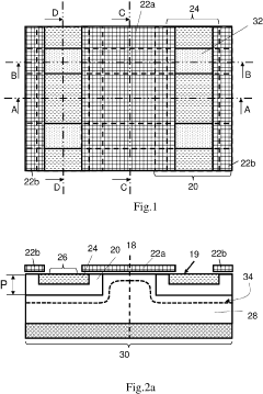
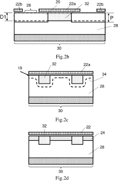
Sic mosfet with transverse p+ region
PatentActiveUS20230053874A1
Innovation
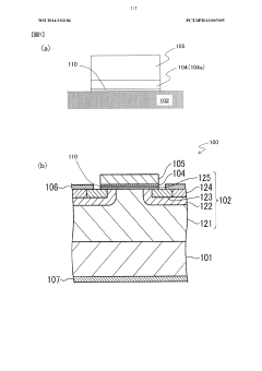
- The design incorporates a silicon carbide MOSFET structure with specific doping layers and geometries, including a polysilicon gate layer, to enhance the protection of the gate oxide without increasing the MOSFET cell area, utilizing epitaxy and ion implantation processes to create N+ and P+ regions that act as shields, ensuring adequate body diode performance and channel mobility.
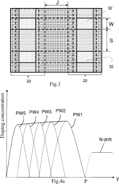
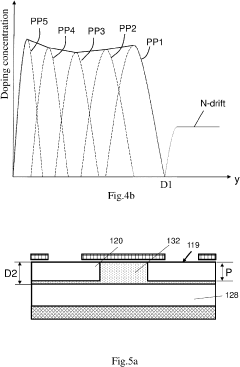
Silicon carbide semiconductor device and method for manufacturing same
PatentWO2014103186A1
Innovation
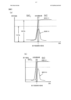
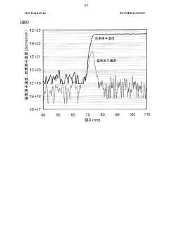
- A silicon carbide semiconductor device with a carbon transition layer between the SiC semiconductor layer and the silicon oxide film, where the nitrogen atom concentration is set to a ratio of 0.11 or more with respect to the carbon atom concentration in the region closer to the silicon oxide film, effectively terminating residual carbon and reducing threshold fluctuations.
Standardization and Qualification Requirements
The standardization and qualification of SiC MOSFETs represent critical frameworks that ensure reliability and performance consistency across different manufacturers and applications. Currently, several international organizations are actively developing and refining standards specifically for SiC power devices, including the JEDEC JC-70 committee, IEC, and automotive standards bodies like AEC-Q101.
JEDEC's JC-70 committee has established specialized working groups focused on wide bandgap semiconductors, with particular attention to SiC MOSFET qualification procedures. These standards address unique characteristics of SiC devices, including higher operating temperatures, faster switching speeds, and different failure mechanisms compared to traditional silicon devices. The qualification requirements typically include extended high-temperature operating life (HTOL) tests, temperature cycling, and gate stress tests specifically calibrated for SiC technology.
The Automotive Electronics Council's AEC-Q101 qualification, originally developed for silicon devices, has been adapted with additional requirements for SiC MOSFETs. These modifications include more stringent temperature cycling (-55°C to 175°C or higher), extended high-temperature reverse bias (HTRB) testing, and specialized gate oxide integrity tests. Automotive applications demand particularly robust qualification procedures due to the harsh operating environments and long expected lifetimes.
For industrial applications, IEC standards provide guidelines for SiC device testing and qualification. The IEC 60747 series has been expanded to include specific provisions for wide bandgap semiconductors, addressing their unique electrical characteristics and reliability concerns. These standards define test methods for parameters such as short-circuit withstand capability, which is particularly important for SiC MOSFETs in power conversion applications.
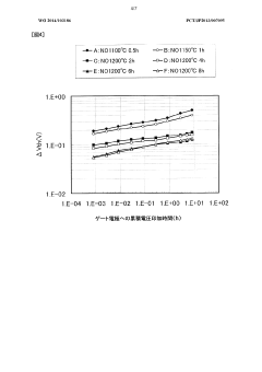
Standardized testing protocols for SiC-specific failure mechanisms are still evolving. Current qualification frameworks are incorporating tests for threshold voltage instability, body diode degradation, and gate oxide reliability—all known challenges for SiC technology. The time-dependent dielectric breakdown (TDDB) testing has been modified to account for the different physics of failure in SiC gate oxides compared to silicon devices.
Manufacturers and end-users often supplement standard qualification requirements with application-specific testing. This includes power cycling with realistic mission profiles, surge current capability assessment, and accelerated aging under combined stresses (temperature, voltage, and switching conditions). These customized qualification approaches help bridge the gap between standardized testing and real-world reliability requirements.
As SiC MOSFET technology continues to mature, qualification standards are expected to evolve further, with increasing harmonization between different standards bodies and more specific guidelines for emerging failure modes. The development of these standards represents a critical enabler for broader SiC adoption across various industries, from electric vehicles to renewable energy systems and industrial power conversion.
JEDEC's JC-70 committee has established specialized working groups focused on wide bandgap semiconductors, with particular attention to SiC MOSFET qualification procedures. These standards address unique characteristics of SiC devices, including higher operating temperatures, faster switching speeds, and different failure mechanisms compared to traditional silicon devices. The qualification requirements typically include extended high-temperature operating life (HTOL) tests, temperature cycling, and gate stress tests specifically calibrated for SiC technology.
The Automotive Electronics Council's AEC-Q101 qualification, originally developed for silicon devices, has been adapted with additional requirements for SiC MOSFETs. These modifications include more stringent temperature cycling (-55°C to 175°C or higher), extended high-temperature reverse bias (HTRB) testing, and specialized gate oxide integrity tests. Automotive applications demand particularly robust qualification procedures due to the harsh operating environments and long expected lifetimes.
For industrial applications, IEC standards provide guidelines for SiC device testing and qualification. The IEC 60747 series has been expanded to include specific provisions for wide bandgap semiconductors, addressing their unique electrical characteristics and reliability concerns. These standards define test methods for parameters such as short-circuit withstand capability, which is particularly important for SiC MOSFETs in power conversion applications.
Standardized testing protocols for SiC-specific failure mechanisms are still evolving. Current qualification frameworks are incorporating tests for threshold voltage instability, body diode degradation, and gate oxide reliability—all known challenges for SiC technology. The time-dependent dielectric breakdown (TDDB) testing has been modified to account for the different physics of failure in SiC gate oxides compared to silicon devices.
Manufacturers and end-users often supplement standard qualification requirements with application-specific testing. This includes power cycling with realistic mission profiles, surge current capability assessment, and accelerated aging under combined stresses (temperature, voltage, and switching conditions). These customized qualification approaches help bridge the gap between standardized testing and real-world reliability requirements.
As SiC MOSFET technology continues to mature, qualification standards are expected to evolve further, with increasing harmonization between different standards bodies and more specific guidelines for emerging failure modes. The development of these standards represents a critical enabler for broader SiC adoption across various industries, from electric vehicles to renewable energy systems and industrial power conversion.
Thermal Management Strategies for SiC Devices
Thermal management is a critical aspect of SiC MOSFET reliability, as these devices often operate at higher power densities and temperatures than their silicon counterparts. The superior thermal conductivity of SiC (approximately 3-4 times that of silicon) enables these devices to handle higher power densities, but also necessitates sophisticated thermal management strategies to ensure optimal performance and longevity.
Traditional cooling methods such as forced air convection prove insufficient for high-power SiC applications. Advanced liquid cooling systems, including direct liquid cooling and microchannel cooling, have emerged as effective solutions. These systems can dissipate heat more efficiently, with thermal resistances as low as 0.1°C/W compared to 0.5-1.0°C/W for conventional air cooling methods.
Novel thermal interface materials (TIMs) play a crucial role in SiC device cooling. Graphene-based TIMs and metal-matrix composites demonstrate thermal conductivities exceeding 10 W/m·K, significantly outperforming traditional silicone-based materials (1-5 W/m·K). These advanced TIMs reduce thermal resistance at critical interfaces, minimizing temperature gradients across the package.
Integrated thermal management approaches, combining die-attach technologies with advanced packaging, show promising results. Silver sintering die-attach technologies provide thermal conductivities up to 240 W/m·K, compared to conventional solder materials (50-70 W/m·K). These technologies reduce thermal resistance by approximately 30-40%, directly improving device reliability by lowering operating temperatures.
Dynamic thermal management strategies, including active temperature monitoring and adaptive power control, are becoming essential for SiC MOSFETs. Real-time junction temperature estimation techniques using temperature-sensitive electrical parameters (TSEPs) enable precise thermal monitoring without additional sensors. These systems can adjust operating parameters based on thermal conditions, preventing thermal runaway scenarios.
Thermal simulation and modeling tools have evolved to address the unique challenges of SiC devices. Multi-physics simulation platforms now incorporate accurate SiC material properties and can model complex thermal-mechanical-electrical interactions. These tools enable designers to predict hotspots and optimize thermal management solutions before physical prototyping, reducing development cycles by up to 40%.
The implementation of these thermal management strategies has demonstrated significant improvements in SiC MOSFET reliability metrics. Field data indicates a 2-3x increase in mean time to failure (MTTF) when advanced thermal solutions are employed, directly addressing thermal-related failure mechanisms such as bond wire lift-off and die-attach degradation that commonly affect SiC devices under thermal stress.
Unlock deeper insights with Patsnap Eureka Quick Research — get a full tech report to explore trends and direct your research. Try now!
Generate Your Research Report Instantly with AI Agent
Supercharge your innovation with Patsnap Eureka AI Agent Platform!