SiC MOSFETs In Aerospace Power Electronics Systems
SEP 5, 20259 MIN READ
Generate Your Research Report Instantly with AI Agent
Patsnap Eureka helps you evaluate technical feasibility & market potential.
SiC MOSFETs Evolution and Aerospace Applications
Silicon Carbide (SiC) MOSFETs have undergone significant evolution since their initial development in the early 1990s. The first commercial SiC MOSFETs emerged around 2011, marking a pivotal shift in power electronics capabilities. These early devices offered switching speeds and thermal performance that surpassed traditional silicon-based counterparts, though reliability concerns and high production costs initially limited widespread adoption in aerospace applications.
The evolution trajectory accelerated between 2015-2020, with manufacturers achieving critical breakthroughs in channel mobility and gate oxide reliability. This period saw the transition from first-generation devices with relatively high on-resistance to second-generation SiC MOSFETs featuring dramatically improved performance metrics. The reduction in specific on-resistance (RDS(on)) by approximately 80% during this period represented a fundamental advancement that expanded the practical application envelope for aerospace systems.
By 2018, third-generation SiC MOSFETs began incorporating advanced trench gate structures, further enhancing power density capabilities while simultaneously improving radiation hardness—a critical parameter for space applications. This evolutionary step enabled the first high-reliability SiC power modules specifically designed for satellite power systems and upper-stage launch vehicle electronics.
The aerospace sector has been particularly influential in driving SiC MOSFET development requirements. The extreme operating conditions of space environments—including wide temperature ranges (-55°C to +125°C), radiation exposure, and ultra-high reliability demands—have pushed manufacturers to develop specialized screening and qualification protocols. The JEDEC JC-70 committee's establishment of specific qualification standards for wide bandgap semiconductors in aerospace applications has formalized many of these requirements.
Current state-of-the-art SiC MOSFETs for aerospace applications feature breakdown voltages ranging from 650V to 1700V, with specialized variants reaching 3300V for high-power propulsion systems. The continuous refinement of die-attach technologies and packaging solutions has addressed early concerns regarding thermal cycling reliability, with modern aerospace-grade devices demonstrating survival capabilities exceeding 1000 thermal cycles between temperature extremes.
Looking forward, the evolution path of aerospace SiC MOSFETs is trending toward higher integration, with embedded gate drivers and protection circuitry becoming standard features. The development of radiation-hardened gate driver ICs specifically optimized for SiC switching characteristics represents a parallel evolutionary track that is enhancing overall system reliability. Additionally, manufacturers are exploring novel epitaxial growth techniques to reduce defect densities, potentially enabling larger die sizes and higher current ratings for next-generation space power systems.
Market Analysis for Aerospace Power Electronics
The aerospace power electronics market is experiencing significant growth, driven by increasing demand for more efficient and reliable power management systems in aircraft, satellites, and space vehicles. Currently valued at approximately $2.8 billion, this market is projected to reach $4.5 billion by 2028, representing a compound annual growth rate of 8.3%. This growth is primarily fueled by the rising number of satellite launches, expansion of commercial aviation, and increasing investments in defense aerospace programs globally.
Silicon Carbide (SiC) MOSFETs are rapidly gaining traction within this market segment due to their superior performance characteristics compared to traditional silicon-based components. The adoption of SiC technology in aerospace power electronics is expected to grow at a rate of 17% annually, outpacing the overall market growth as manufacturers increasingly recognize the benefits of these advanced semiconductors.
Key market drivers include the industry-wide push toward more electric aircraft (MEA) architectures, which aim to replace hydraulic and pneumatic systems with electrical alternatives. This transition requires power electronics capable of handling higher voltages, temperatures, and switching frequencies – precisely where SiC MOSFETs excel. Additionally, the growing emphasis on reducing aircraft weight and improving fuel efficiency creates strong demand for the compact, lightweight power conversion systems enabled by SiC technology.
Regional analysis reveals North America currently dominates the aerospace SiC market with approximately 42% market share, followed by Europe (31%) and Asia-Pacific (21%). However, the Asia-Pacific region is expected to witness the fastest growth over the next five years due to increasing aerospace manufacturing activities in China, Japan, and India.
Customer segmentation shows that major aerospace OEMs and tier-1 suppliers constitute the largest market segment, accounting for 65% of SiC MOSFET implementations in aerospace applications. Defense contractors represent 25% of the market, while commercial space companies account for the remaining 10%, though this latter segment is growing rapidly with the expansion of private space ventures.
Price sensitivity analysis indicates that while SiC components command a premium of 2.5-3x over silicon alternatives, the total cost of ownership benefits – including reduced cooling requirements, higher power density, and improved reliability – are increasingly justifying this premium for aerospace applications where performance and reliability are paramount.
Technical Barriers and Development Status
Despite the promising potential of SiC MOSFETs in aerospace power electronics systems, several significant technical barriers currently impede their widespread adoption. The primary challenge remains the reliability concerns under extreme aerospace conditions. SiC MOSFETs must withstand radiation exposure, wide temperature fluctuations (-55°C to over 300°C), and vacuum environments while maintaining consistent performance characteristics. Current devices show threshold voltage instability and increased leakage currents after radiation exposure, particularly problematic for mission-critical aerospace applications.
Manufacturing consistency presents another substantial hurdle. The production of high-quality SiC wafers with minimal defects remains difficult to scale, resulting in higher costs and yield variations. Crystal defects such as micropipes, dislocations, and stacking faults in SiC substrates directly impact device performance and reliability, creating inconsistencies across production batches that aerospace standards cannot tolerate.
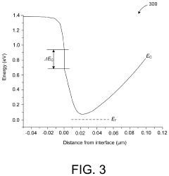
Gate oxide reliability constitutes a persistent technical challenge. The interface between SiC and SiO2 exhibits higher defect densities compared to traditional silicon interfaces, leading to reduced channel mobility and reliability concerns. These interface traps cause threshold voltage shifts and accelerated aging under high-temperature operation, particularly problematic for long-duration space missions requiring years of uninterrupted operation.
The current development status shows promising advancements despite these challenges. Leading manufacturers including Wolfspeed, ROHM, and STMicroelectronics have developed aerospace-grade SiC MOSFETs with improved radiation hardness and temperature stability. Recent devices demonstrate operation at junction temperatures up to 250°C with significantly reduced on-resistance compared to silicon alternatives, enabling higher power density solutions.
Research institutions and aerospace organizations worldwide are actively addressing reliability concerns through accelerated life testing and physics-of-failure modeling. NASA and ESA have established specialized qualification protocols for SiC devices in space applications, while academic-industry partnerships focus on improving gate oxide quality and interface characteristics through novel processing techniques.
Geographically, SiC MOSFET development for aerospace applications remains concentrated in the United States, Europe, and Japan, with emerging capabilities in China. The U.S. maintains leadership through significant Department of Defense and NASA investments, while European efforts are coordinated through ESA and Horizon Europe programs focusing on radiation-hardened designs. Japanese manufacturers excel in high-temperature packaging solutions, while Chinese development focuses on cost reduction and domestic supply chain establishment.
Current SiC MOSFET Implementation Strategies
01 SiC MOSFET structure and fabrication
Silicon Carbide (SiC) MOSFETs have unique structural designs and fabrication methods that enhance their performance characteristics. These include specialized gate structures, channel formations, and doping profiles that contribute to improved electron mobility and reduced on-resistance. Advanced fabrication techniques help minimize interface defects between the SiC substrate and gate oxide, which is crucial for reliable operation at high temperatures and voltages.- SiC MOSFET structure and fabrication: Silicon Carbide (SiC) MOSFETs have unique structural features and fabrication methods that enhance their performance characteristics. These include specialized gate structures, channel designs, and manufacturing techniques that improve electron mobility and reduce on-resistance. The fabrication process often involves specific thermal oxidation steps, ion implantation methods, and annealing processes tailored for SiC material to achieve optimal device performance and reliability.
- SiC MOSFET power applications and circuits: SiC MOSFETs are widely used in power electronic applications due to their superior performance at high voltages and temperatures. These devices are incorporated into various circuit topologies including power converters, inverters, and motor drives. The implementation of SiC MOSFETs in these applications results in higher efficiency, reduced switching losses, and smaller form factors compared to traditional silicon-based solutions.
- Gate driver designs for SiC MOSFETs: Specialized gate driver circuits are essential for optimal operation of SiC MOSFETs. These drivers are designed to handle the unique switching characteristics and gate voltage requirements of SiC devices. Advanced gate driver designs incorporate features such as adjustable slew rates, protection mechanisms against voltage spikes, and temperature compensation to ensure reliable operation across various operating conditions.
- Thermal management and reliability of SiC MOSFETs: Effective thermal management is crucial for SiC MOSFETs to maintain reliability and performance. Various techniques are employed including advanced packaging solutions, heat sink designs, and thermal interface materials specifically optimized for SiC devices. These approaches help dissipate the heat generated during high-power operation and extend the device lifetime. Reliability enhancement methods also include specialized passivation layers and edge termination structures to improve robustness under extreme operating conditions.
- SiC MOSFET integration and system optimization: Integration of SiC MOSFETs into electronic systems requires specialized design considerations to maximize their benefits. This includes optimized PCB layouts, parasitic inductance minimization techniques, and system-level design approaches that account for the fast switching speeds of SiC devices. Advanced control algorithms and protection schemes are also developed to ensure stable operation and prevent device failures in complex power systems utilizing SiC MOSFETs.
02 Power conversion applications of SiC MOSFETs
SiC MOSFETs are extensively used in power conversion systems due to their superior switching characteristics and high-temperature operation capabilities. These devices enable more efficient power conversion in applications such as inverters, converters, and power supplies. The implementation of SiC MOSFETs in these systems results in reduced switching losses, higher operating frequencies, and improved thermal management, leading to more compact and efficient power electronic systems.Expand Specific Solutions03 Gate driver designs for SiC MOSFETs
Specialized gate driver circuits are essential for optimal operation of SiC MOSFETs. These drivers are designed to handle the unique switching characteristics and gate voltage requirements of SiC devices. Advanced gate driver designs incorporate features such as adjustable slew rates, protection against voltage spikes, and temperature compensation mechanisms. These features help maximize switching efficiency while protecting the device from operational stresses.Expand Specific Solutions04 Thermal management and reliability of SiC MOSFETs
Effective thermal management is crucial for the reliability and performance of SiC MOSFETs. Various packaging technologies and cooling solutions are employed to dissipate heat efficiently from these high-power devices. Additionally, reliability enhancement techniques address issues such as threshold voltage instability, gate oxide integrity, and body diode performance. These approaches extend the operational lifetime of SiC MOSFETs in demanding applications with high temperature and switching stress conditions.Expand Specific Solutions05 Circuit integration and system applications
SiC MOSFETs are increasingly integrated into complex circuit designs and system applications. This integration involves specialized circuit topologies that leverage the unique characteristics of SiC devices. Applications include electric vehicle powertrains, renewable energy systems, industrial motor drives, and high-frequency power supplies. The integration of SiC MOSFETs in these systems requires careful consideration of parasitic elements, electromagnetic interference, and system-level reliability to fully realize the benefits of SiC technology.Expand Specific Solutions
Leading Manufacturers and Competitive Landscape
The SiC MOSFET market in aerospace power electronics is experiencing rapid growth, currently in an early maturity phase with increasing adoption across critical aerospace applications. Market size is expanding significantly, driven by demands for higher efficiency, temperature resistance, and power density in aerospace systems. Technology maturity varies among key players, with Wolfspeed and ROHM leading commercial deployment, while Mitsubishi Electric and GeneSiC demonstrate strong manufacturing capabilities. Academic institutions like Xidian University and University of Warwick are advancing fundamental research, while aerospace specialists such as GE Aviation Systems and China Academy of Space Technology focus on application-specific implementations. State Grid and other power electronics companies are accelerating development to meet stringent aerospace reliability requirements, creating a competitive landscape balanced between established semiconductor manufacturers and emerging specialized players.
Wolfspeed, Inc.
Technical Solution: Wolfspeed has pioneered silicon carbide (SiC) MOSFETs specifically designed for aerospace power electronics systems, offering industry-leading power density and efficiency. Their aerospace-grade SiC MOSFETs feature high-temperature operation capabilities (up to 225°C junction temperature), radiation hardening for space applications, and ultra-low switching losses. Wolfspeed's vertical integration approach—controlling the entire supply chain from SiC wafer production to device packaging—ensures reliability critical for aerospace applications. Their latest generation devices achieve on-resistance as low as 2.6 mΩ·cm² with blocking voltages of 1200V and 1700V, enabling significant size and weight reductions in aerospace power conversion systems. The company has developed specialized packaging solutions that address thermal management challenges unique to aerospace environments, including hermetically sealed packages that maintain integrity under extreme conditions.
Strengths: Industry-leading power density and efficiency; complete vertical integration from substrate to packaging; extensive aerospace qualification heritage; superior high-temperature performance. Weaknesses: Higher initial cost compared to silicon alternatives; limited production capacity to meet growing aerospace demand; more complex gate drive requirements than traditional silicon devices.
GeneSiC Semiconductor LLC
Technical Solution: GeneSiC Semiconductor has developed specialized SiC MOSFETs for aerospace power electronics with a focus on radiation hardness and reliability in extreme environments. Their aerospace-grade SiC MOSFETs feature enhanced single event effect (SEE) immunity and total ionizing dose (TID) tolerance exceeding 300 krad, making them suitable for satellite and deep space applications. GeneSiC's proprietary trench MOSFET design achieves lower specific on-resistance (2.5 mΩ·cm²) while maintaining robust short-circuit capability (>10μs at 175°C). Their devices incorporate advanced termination structures that ensure stable performance across the wide temperature ranges (-55°C to +225°C) encountered in aerospace applications. GeneSiC has also pioneered hermetically sealed packaging solutions with enhanced thermal cycling capability (>1000 cycles from -55°C to +150°C) to meet the stringent reliability requirements of aerospace systems.
Strengths: Superior radiation hardness specifically engineered for space applications; excellent thermal cycling capability; robust short-circuit withstand capability; wide temperature range operation. Weaknesses: Smaller production scale compared to larger competitors; less extensive flight heritage data compared to established aerospace suppliers; higher cost structure due to specialized radiation-hardened processes.
Key Patents and Research Breakthroughs
Silicon carbide metal oxide semiconductor field effect transistor and manufacturing method of silicon carbide metal oxide semiconductor field effect transistor
PatentPendingUS20230378341A1
Innovation
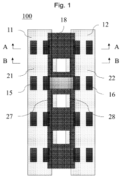
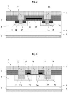
- The design incorporates alternating cells with specific well regions, source regions, and contact layers, including ohmic and Schottky contacts, to reduce channel density, enhance short-circuit tolerance, and minimize reverse leakage current and forward voltage drop, while maintaining the transistor's size and functionality.
Silicon carbide field-effect transistors
PatentActiveUS11894454B2
Innovation
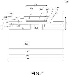
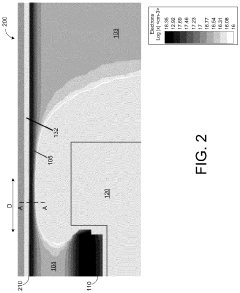
- The development of a silicon carbide (SiC) metal-oxide-semiconductor field-effect transistor (MOSFET) with a gate structure comprising a gate oxide layer, an aluminum nitride layer, and a p-type gallium nitride layer, which includes a lateral built-in channel with a p-type AlGaN gate and an AlN buffer layer, providing high threshold voltage and low interface trap density, enabling efficient operation with low on-state resistance.
Reliability and Radiation Hardness Assessment
Reliability and radiation hardness are critical considerations for SiC MOSFETs in aerospace power electronics systems, where components must withstand extreme environmental conditions and radiation exposure. SiC MOSFETs demonstrate superior reliability compared to traditional silicon devices, with significantly higher breakdown field strength (approximately 10 times that of Si) and thermal conductivity (3 times higher than Si), enabling operation at temperatures exceeding 200°C.
The reliability assessment of SiC MOSFETs involves rigorous testing protocols including high-temperature gate bias (HTGB), high-temperature reverse bias (HTRB), and temperature humidity bias (THB) tests. Recent studies indicate that commercial SiC MOSFETs can maintain stable performance for over 1000 hours under HTGB conditions at 175°C, with threshold voltage shifts below 0.5V. This stability is crucial for aerospace applications where consistent performance over extended missions is mandatory.
Radiation hardness testing reveals that SiC MOSFETs exhibit inherent resistance to total ionizing dose (TID) effects due to the wider bandgap (3.26 eV compared to 1.12 eV for Si). Tests conducted by NASA and ESA demonstrate that SiC devices can withstand radiation doses up to 300 krad(Si) with minimal parametric degradation, making them suitable for Earth orbit and deep space missions.
Single event effects (SEEs) remain a concern, particularly single event burnout (SEB) and single event gate rupture (SEGR). Research indicates that SiC MOSFETs have higher critical linear energy transfer (LET) thresholds than Si counterparts, with values typically exceeding 15 MeV·cm²/mg. However, vulnerability increases at higher operating voltages, necessitating derating strategies for aerospace implementations.
Accelerated life testing data suggests that SiC MOSFETs have a projected operational lifetime exceeding 15 years under aerospace conditions, with failure rates below 10 FIT (failures in time, per billion device hours). The primary failure mechanisms identified include gate oxide degradation, threshold voltage instability, and body diode degradation after repeated avalanche events.
Recent advancements in packaging technology, including high-temperature die-attach materials and hermetic sealing techniques, have further enhanced the reliability of SiC power modules for aerospace applications. Specialized screening procedures, including burn-in testing at 250°C and neutron irradiation testing, are being implemented by manufacturers to qualify devices for mission-critical aerospace systems.
The combined reliability and radiation hardness advantages of SiC MOSFETs translate to significant system-level benefits, including reduced cooling requirements, higher power density, and enhanced mission capabilities for aerospace power electronics systems operating in extreme environments.
Aerospace Certification Standards and Compliance
The aerospace industry imposes stringent certification requirements for electronic components used in flight systems, creating a complex regulatory landscape for SiC MOSFET implementation. DO-254 (Design Assurance Guidance for Airborne Electronic Hardware) serves as the primary certification framework, establishing five design assurance levels (DAL A through E) based on failure consequence severity. Power electronics systems utilizing SiC MOSFETs typically require DAL A or B certification, demanding extensive documentation, verification, and validation processes.
The European Aviation Safety Agency (EASA) and the Federal Aviation Administration (FAA) maintain slightly different certification approaches, though both recognize DO-160 environmental testing standards. These standards subject SiC MOSFETs to rigorous environmental stress screening including temperature cycling (-55°C to +125°C), vibration testing, and radiation hardness assessment—particularly critical for components deployed in high-altitude or space applications.
Radiation effects present unique certification challenges for SiC power devices. While inherently more radiation-resistant than silicon counterparts, SiC MOSFETs must still undergo Single Event Effects (SEE) and Total Ionizing Dose (TID) testing. NASA's EEE-INST-002 and ESA's European Space Components Coordination (ESCC) specifications provide detailed qualification procedures for space-grade components, requiring manufacturers to demonstrate reliability under cosmic radiation exposure.
Thermal management certification represents another critical compliance area. MIL-STD-750 test methods specifically address power semiconductor thermal characterization, while MIL-STD-883 covers environmental and mechanical testing. SiC MOSFET manufacturers must provide detailed thermal resistance data and demonstrate reliable operation under extreme temperature conditions to achieve certification.
The certification process typically extends 18-24 months for new SiC MOSFET implementations in aerospace systems, significantly longer than commercial qualification cycles. This timeline includes extensive reliability demonstration testing (RDT) where devices undergo accelerated life testing at elevated temperatures and voltages to verify long-term reliability. Failure analysis and physics-of-failure modeling are mandatory components of the certification package.
Recent developments include the creation of specialized qualification standards for wide bandgap semiconductors. The JEDEC JC-70 committee has established testing protocols specifically addressing SiC MOSFET reliability concerns, including gate oxide integrity and body diode stability. These standards are increasingly referenced in aerospace certification processes, providing a standardized framework for evaluating next-generation power devices in mission-critical applications.
Unlock deeper insights with Patsnap Eureka Quick Research — get a full tech report to explore trends and direct your research. Try now!
Generate Your Research Report Instantly with AI Agent
Supercharge your innovation with Patsnap Eureka AI Agent Platform!
