

How Do SiC MOSFETs Improve Efficiency In Power Converters?
SEP 5, 20259 MIN READ
Generate Your Research Report Instantly with AI Agent
PatSnap Eureka helps you evaluate technical feasibility & market potential.
SiC MOSFET Technology Evolution and Objectives
Silicon Carbide (SiC) MOSFET technology represents one of the most significant advancements in power electronics over the past two decades. The evolution of this wide bandgap semiconductor technology began in the early 2000s when researchers identified SiC's potential to overcome the limitations of traditional silicon-based power devices. With a bandgap of 3.26 eV compared to silicon's 1.12 eV, SiC offers fundamentally superior physical properties that enable higher temperature operation, faster switching speeds, and lower conduction losses.
The historical progression of SiC MOSFETs has been marked by continuous improvements in manufacturing processes, device design, and material quality. Initial commercialization efforts faced significant challenges related to substrate quality, defect density, and gate oxide reliability. However, persistent research and development have led to remarkable advancements in these areas, with defect densities decreasing by orders of magnitude and device performance steadily improving.
From 2010 to 2015, the industry witnessed the first generation of commercially viable SiC MOSFETs, primarily targeting niche applications where performance advantages could justify the higher cost. The period from 2015 to 2020 saw dramatic improvements in manufacturing scale and cost reduction, expanding the application scope to automotive, industrial, and renewable energy sectors.
The primary technical objective of SiC MOSFET development has been to maximize power conversion efficiency while minimizing system size and cost. This involves reducing on-resistance (RDS(on)), improving switching characteristics, enhancing thermal performance, and ensuring long-term reliability. Current state-of-the-art devices achieve specific on-resistance values approaching the theoretical material limits, with switching speeds that enable operation at frequencies several times higher than silicon counterparts.
Looking forward, the technology roadmap for SiC MOSFETs includes several key objectives: further reduction in manufacturing costs to achieve price parity with silicon devices in more applications; development of higher voltage ratings beyond the current 1700V standard offerings; improvement in channel mobility to reduce conduction losses; and enhanced packaging technologies to fully leverage SiC's thermal capabilities.
The convergence of these technological advancements with growing market demands for energy efficiency, particularly in electric vehicles, renewable energy systems, and industrial applications, creates a compelling trajectory for SiC MOSFET adoption. The technology is increasingly positioned as a critical enabler for next-generation power electronics systems where efficiency, power density, and reliability are paramount considerations.
Market Demand Analysis for High-Efficiency Power Converters
The global market for high-efficiency power converters has experienced substantial growth in recent years, driven primarily by increasing demands for energy-efficient solutions across multiple industries. The power electronics market, within which SiC MOSFET-based converters represent a growing segment, was valued at approximately $40 billion in 2022 and is projected to reach $65 billion by 2028, with a compound annual growth rate exceeding 7%.
Several key factors are fueling this market expansion. First, stringent government regulations worldwide are mandating improved energy efficiency standards for electronic devices and power systems. The European Union's Ecodesign Directive, for instance, requires power supplies to meet minimum efficiency thresholds, while similar regulations in the United States through Energy Star and in China through their Energy Conservation Law are pushing manufacturers toward higher-efficiency solutions.
The electric vehicle (EV) sector represents one of the most significant growth drivers for SiC MOSFET-based power converters. With global EV sales surpassing 10 million units in 2022 and projected to reach 30 million by 2030, the demand for efficient power conversion systems that maximize battery life and reduce charging times continues to accelerate. SiC MOSFETs enable smaller, lighter onboard chargers and more efficient power inverters, directly addressing key consumer concerns about EV range and performance.
Renewable energy systems constitute another major market segment. The global solar PV capacity additions reached 239 GW in 2022, while wind power installations exceeded 93 GW. Both sectors require highly efficient power converters to maximize energy harvest and grid integration. SiC-based inverters can achieve efficiency ratings above 99%, compared to 96-97% for traditional silicon-based solutions, translating to significant energy savings at utility scale.
Industrial applications represent a third substantial market, with factory automation, motor drives, and uninterruptible power supplies increasingly adopting SiC technology. The industrial motor drives market alone was valued at $14 billion in 2022, with efficiency-focused upgrades driving significant portions of this spending.
Data centers, which consume approximately 1-2% of global electricity, are increasingly focused on power efficiency metrics like Power Usage Effectiveness (PUE). With electricity costs representing 20-40% of operational expenses in data centers, the improved efficiency offered by SiC-based power systems directly impacts bottom-line performance.
Consumer electronics manufacturers are also exploring SiC-based solutions for fast chargers and power adapters, driven by consumer demand for faster charging times and smaller form factors. This segment is expected to grow as SiC component costs decrease through economies of scale and manufacturing improvements.
Current SiC MOSFET Technology Landscape and Challenges
Silicon Carbide (SiC) MOSFET technology has rapidly evolved over the past decade, establishing itself as a transformative force in power electronics. Currently, commercial SiC MOSFETs are available with blocking voltages ranging from 650V to 1700V, with research prototypes demonstrating capabilities up to 10kV. These devices have achieved on-resistance values as low as 2.5 mΩ·cm², significantly outperforming their silicon counterparts in high-voltage applications.
The global SiC power device market reached approximately $1.1 billion in 2021 and is projected to exceed $6 billion by 2027, with a compound annual growth rate of over 30%. This growth is primarily driven by electric vehicle applications, which account for nearly 60% of the market, followed by industrial power supplies, renewable energy systems, and rail transportation.
Despite impressive advancements, SiC MOSFET technology faces several critical challenges. The most significant technical hurdle remains the SiC/SiO₂ interface quality, which exhibits higher defect densities compared to Si/SiO₂ interfaces. These defects lead to reduced channel mobility, threshold voltage instability, and reliability concerns under high-temperature operation. Current interface trap densities typically range from 10¹¹ to 10¹² cm⁻² eV⁻¹, still higher than the 10¹⁰ cm⁻² eV⁻¹ commonly achieved in silicon devices.
Manufacturing challenges persist in substrate quality and wafer size. While 6-inch SiC wafers have become standard, the industry is transitioning to 8-inch wafers to improve economies of scale. However, defect densities in these larger wafers remain problematic, with typical values of 1-5 defects/cm² compared to less than 0.1 defects/cm² in mature silicon technology. These defects directly impact device yield and manufacturing costs.
Cost remains a significant barrier to wider adoption. SiC MOSFETs typically command a 2-3x price premium over silicon alternatives, though this gap has narrowed from the 5-10x premium seen five years ago. The high cost stems from expensive substrate materials, complex manufacturing processes, and lower yields compared to silicon technologies.
Packaging technology presents another challenge for SiC MOSFETs. Traditional packaging solutions often limit the full performance potential of SiC devices, particularly in terms of thermal management and parasitic inductance. Advanced packaging technologies like silver sintering and direct bonded copper are being developed to address these limitations, but they add complexity and cost to the manufacturing process.
Geographically, SiC MOSFET technology development is concentrated in the United States, Europe, Japan, and increasingly China. Key research institutions include Cree/Wolfspeed's research center in North Carolina, ROHM's facilities in Japan, and the Fraunhofer Institute in Germany, with China rapidly expanding its research capabilities through significant government investment.
Technical Implementation of SiC MOSFETs in Power Converters
01 SiC MOSFET device structure optimization
Silicon Carbide (SiC) MOSFET efficiency can be improved through structural optimizations of the device. These optimizations include enhanced gate designs, improved channel mobility, reduced on-resistance, and optimized drift regions. By refining the physical structure of SiC MOSFETs, manufacturers can achieve higher switching speeds, lower conduction losses, and better thermal performance, all contributing to overall improved efficiency in power conversion applications.- SiC MOSFET device structure optimization: Optimizing the device structure of Silicon Carbide (SiC) MOSFETs can significantly improve efficiency. This includes modifications to the gate structure, channel design, and drift region engineering. Advanced structures like trench gates, double-implanted MOSFETs, and optimized junction terminations reduce on-resistance and switching losses, leading to higher power conversion efficiency. These structural improvements help minimize parasitic capacitances and resistances that typically limit performance in power applications.
- Gate drive and control techniques: Specialized gate drive circuits and control techniques are essential for maximizing SiC MOSFET efficiency. These include optimized gate voltage levels, advanced switching timing control, and specialized driver ICs designed specifically for SiC devices. Proper gate drive design helps to reduce switching losses, prevent parasitic turn-on, and manage the faster switching speeds inherent to SiC technology. Intelligent gate control algorithms can dynamically adjust switching parameters based on operating conditions.
- Thermal management solutions: Effective thermal management is crucial for maintaining SiC MOSFET efficiency at high power levels. Advanced cooling techniques, optimized packaging designs, and improved thermal interface materials help dissipate heat more effectively. This allows SiC MOSFETs to operate at higher power densities while maintaining reliability and efficiency. Solutions include direct liquid cooling, advanced heat sink designs, and thermally optimized module packaging that minimize thermal resistance from junction to ambient.
- Power converter topology optimization: Optimizing power converter topologies specifically for SiC MOSFETs can significantly enhance overall system efficiency. This includes redesigning circuit layouts to minimize parasitic inductances, implementing soft-switching techniques, and developing novel converter architectures that leverage SiC's fast switching capabilities. Advanced topologies like multilevel converters, resonant circuits, and hybrid approaches combining different semiconductor technologies can maximize the benefits of SiC MOSFETs while mitigating their limitations.
- Interface and material quality improvements: Enhancing the quality of the SiC/oxide interface and improving material purity are fundamental approaches to increasing SiC MOSFET efficiency. Advanced fabrication techniques, novel dielectric materials, and interface treatments reduce channel resistance and improve carrier mobility. These improvements address the inherently higher defect density at the SiC/oxide interface compared to silicon devices. Techniques include high-temperature annealing processes, alternative gate dielectrics, and specialized channel doping profiles to optimize carrier transport.
02 Gate drive and control techniques
Advanced gate drive and control techniques significantly impact SiC MOSFET efficiency. Optimized gate driving circuits with proper voltage levels, slew rates, and timing can reduce switching losses and prevent parasitic oscillations. Intelligent gate drivers that adapt to operating conditions can further enhance performance by balancing switching speed with electromagnetic interference. These control techniques enable SiC MOSFETs to operate closer to their theoretical efficiency limits in practical applications.Expand Specific Solutions03 Thermal management solutions
Effective thermal management is crucial for maintaining SiC MOSFET efficiency at high power levels. Advanced cooling techniques, optimized packaging designs, and improved thermal interface materials help dissipate heat more effectively. By keeping junction temperatures lower, these solutions prevent efficiency degradation during operation and extend device lifetime. Innovative thermal management approaches enable SiC MOSFETs to operate reliably at higher power densities while maintaining their efficiency advantages.Expand Specific Solutions04 Power conversion circuit topologies
Specialized power conversion circuit topologies can maximize the benefits of SiC MOSFETs. These include resonant and soft-switching topologies that reduce switching losses, multilevel converter designs that distribute stress across multiple devices, and optimized layout techniques that minimize parasitic inductances. By designing circuits specifically to leverage SiC MOSFET characteristics, engineers can achieve higher frequency operation, reduced passive component sizes, and overall system efficiency improvements.Expand Specific Solutions05 SiC MOSFET manufacturing process improvements
Advancements in manufacturing processes directly impact SiC MOSFET efficiency. Improved substrate quality, enhanced epitaxial growth techniques, optimized implantation processes, and refined gate oxide formation methods all contribute to better device performance. These manufacturing improvements result in reduced defect densities, more uniform electrical characteristics, and enhanced reliability. By continually refining production techniques, manufacturers can deliver SiC MOSFETs with progressively better efficiency metrics for power electronics applications.Expand Specific Solutions
Key Manufacturers and Competitive Landscape
SiC MOSFET technology is currently in a growth phase, with the market expanding rapidly due to increasing demand for high-efficiency power conversion solutions in electric vehicles, renewable energy, and industrial applications. The global market size for SiC power devices is projected to reach several billion dollars by 2025, growing at over 25% CAGR. Leading players include established semiconductor manufacturers like Wolfspeed, Infineon Technologies, ROHM, and ON Semiconductor, who have mature product portfolios and manufacturing capabilities. Emerging competitors include Huawei and Chinese institutions like Hunan University and UESTC, who are investing heavily in R&D. The technology has reached commercial maturity for applications below 1700V, with ongoing development for higher voltage ratings and improved reliability.
Fast Sic Semiconductor, Inc.
Technical Solution: Fast SiC has developed innovative SiC MOSFET technology focusing on ultra-fast switching performance while maintaining robustness. Their devices utilize advanced channel engineering to optimize carrier mobility and reduce specific on-resistance. Fast SiC's MOSFETs feature proprietary gate oxide processing techniques that enhance reliability under high-frequency switching conditions. Their technology enables switching frequencies exceeding 200kHz in soft-switching topologies while maintaining high efficiency, allowing for significant miniaturization of power conversion systems. Fast SiC has developed specialized packaging solutions with minimized parasitic inductance, critical for enabling the extremely fast switching speeds of their devices without excessive voltage overshoots. Their SiC MOSFETs demonstrate turn-on and turn-off times below 10ns, enabling new classes of high-frequency power converters with efficiency improvements of 2-3% compared to conventional silicon-based designs operating at lower frequencies.
Strengths: Industry-leading switching speed performance and specialized expertise in high-frequency applications. Weaknesses: Smaller company scale with more limited manufacturing capacity and narrower product portfolio compared to larger competitors.
ROHM Co., Ltd.
Technical Solution: ROHM has pioneered the development of trench-type SiC MOSFETs that feature significantly reduced on-resistance and improved short-circuit withstand capability. Their 4th generation SiC MOSFETs utilize a proprietary double-trench structure that separates the JFET region from the gate, reducing internal resistance while maintaining high reliability. ROHM's technology achieves approximately 40% reduction in switching losses and 50% reduction in conduction losses compared to conventional planar SiC MOSFETs. Their devices incorporate advanced termination structures that enhance breakdown voltage stability and reliability under high-temperature operation. ROHM has also developed specialized packaging technology with optimized thermal performance to maximize the benefits of SiC in power conversion applications, enabling power converters with efficiency exceeding 98% in solar inverter applications.
Strengths: Superior short-circuit withstand capability, excellent thermal performance, and comprehensive design support ecosystem. Weaknesses: Limited product portfolio compared to some competitors and higher cost structure for certain device ratings.
Critical Patents and Innovations in SiC MOSFET Technology
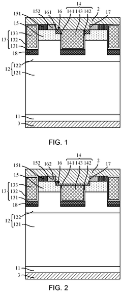
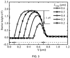
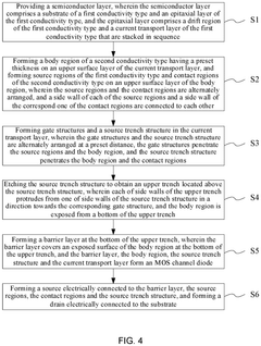
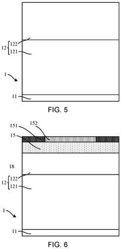
Power mosfet and manufacturing method therefor
PatentPendingEP4539126A1
Innovation
- The power MOSFET design incorporates a semiconductor structure with a source trench structure and an upper trench, where the barrier layer covers the exposed surface of the body region at the bottom of the upper trench, forming an MOS channel diode. The length of the conductive channel is reduced by adjusting the depth of the upper trench, lowering the turn-on voltage and conduction loss.
Thermal Management Solutions for SiC Power Devices
Silicon Carbide (SiC) MOSFETs generate significant heat during operation despite their superior efficiency compared to silicon alternatives. Effective thermal management is therefore critical to ensure optimal performance and longevity of SiC power devices in converter applications.
Traditional cooling methods often prove inadequate for SiC devices operating at higher power densities and temperatures. Advanced thermal management solutions must address the unique characteristics of SiC, including its ability to function at junction temperatures up to 200°C—considerably higher than silicon's typical 150°C limit.
Direct liquid cooling systems represent a significant advancement for SiC thermal management. These systems utilize dielectric fluids in direct contact with semiconductor devices, achieving thermal resistance values below 0.1°C/W. This approach eliminates thermal interface materials that typically create bottlenecks in heat dissipation pathways.
Double-sided cooling architectures have emerged as particularly effective for SiC modules. By extracting heat from both sides of the device, these solutions can reduce thermal resistance by up to 40% compared to conventional single-sided approaches. Implementation requires specialized packaging techniques, including pressure-contact assemblies or sintered connections that maintain thermal performance while accommodating the mechanical stress of thermal cycling.
Advanced thermal interface materials (TIMs) specifically engineered for SiC applications include metal-based TIMs with thermal conductivities exceeding 200 W/mK and phase-change materials that optimize contact at high temperatures. Sintered silver and copper interfaces are gaining prominence, offering thermal conductivities 5-10 times higher than traditional solder materials while withstanding the extreme temperature cycles characteristic of SiC operation.
Integrated cooling solutions that combine multiple approaches are becoming standard in high-performance SiC converters. These hybrid systems might incorporate microfluidic channels directly into device substrates alongside advanced heat spreaders and optimized thermal stacks. Such integration requires careful co-design of electrical, mechanical, and thermal aspects from the earliest development stages.
Computational fluid dynamics (CFD) modeling plays an essential role in optimizing thermal solutions for SiC devices. Advanced simulation tools now account for the unique thermal properties of SiC materials and can predict hotspot formation under various operating conditions. These models enable designers to evaluate cooling solutions before physical prototyping, significantly accelerating development cycles and reducing costs.
Cost-Performance Analysis and Commercial Viability
The cost-performance ratio of SiC MOSFETs presents a complex economic equation for power converter manufacturers. While the initial acquisition cost of SiC MOSFETs remains 2-3 times higher than traditional silicon alternatives, this premium must be evaluated against significant performance advantages that translate to system-level economic benefits. Current market analysis indicates that SiC MOSFET prices have decreased by approximately 10-15% annually over the past five years, gradually improving their commercial viability.
When conducting total cost of ownership (TCO) calculations, SiC-based power converters demonstrate compelling advantages. The enhanced efficiency—typically 2-3% higher than silicon-based systems—translates to substantial energy cost savings over the operational lifetime of the equipment. For high-power applications operating continuously, these savings can offset the initial investment premium within 1-3 years, depending on energy costs and utilization patterns.
The reduced cooling requirements represent another significant cost advantage. SiC MOSFETs' superior thermal performance allows for smaller heatsinks and simplified thermal management systems, reducing both material costs and physical footprint. Studies indicate cooling system cost reductions of 20-40% are achievable in properly optimized designs, contributing to overall system cost competitiveness.
Commercial adoption patterns reveal sector-specific cost-benefit thresholds. Electric vehicle manufacturers have embraced SiC technology most aggressively, as the efficiency gains directly impact critical performance metrics like range and charging speed. Industrial power conversion applications follow closely, particularly in scenarios where equipment operates continuously at high power levels. The renewable energy sector shows increasing adoption rates as system designers prioritize lifetime efficiency over initial capital expenditure.
Manufacturing scalability continues to improve, with major suppliers expanding production capacity significantly between 2020-2023. Wafer size increases from 4-inch to 6-inch and now 8-inch fabrication processes are driving economies of scale. Industry forecasts project that continued manufacturing refinements and increased competition will further reduce the cost premium of SiC MOSFETs to approximately 1.5x that of silicon alternatives by 2025-2026.
The commercial viability assessment must also consider secondary economic benefits, including reduced maintenance requirements, extended system lifespan, and improved reliability metrics. When these factors are incorporated into comprehensive business models, SiC-based power converters increasingly demonstrate favorable return on investment profiles across a widening range of applications and power levels.
Unlock deeper insights with PatSnap Eureka Quick Research — get a full tech report to explore trends and direct your research. Try now!
Generate Your Research Report Instantly with AI Agent
Supercharge your innovation with PatSnap Eureka AI Agent Platform!