What Are The Packaging Challenges In SiC MOSFET Applications?
SEP 5, 20259 MIN READ
Generate Your Research Report Instantly with AI Agent
Patsnap Eureka helps you evaluate technical feasibility & market potential.
SiC MOSFET Packaging Background and Objectives
Silicon Carbide (SiC) MOSFET technology has emerged as a revolutionary advancement in power electronics over the past two decades. The evolution of this wide bandgap semiconductor technology represents a significant shift from traditional silicon-based power devices, offering superior performance characteristics including higher breakdown voltage, faster switching speeds, and better thermal conductivity. Since the early 2000s, SiC MOSFETs have progressed from laboratory curiosities to commercially viable products, with continuous improvements in manufacturing processes and device reliability.
The technological trajectory of SiC MOSFETs has been marked by steady increases in current density, reduction in on-resistance, and enhanced ruggedness. Early generations faced challenges with gate oxide reliability and high defect densities, but recent advancements have largely addressed these issues, enabling widespread adoption across multiple industries.
The primary technical objective in SiC MOSFET packaging development is to create encapsulation solutions that fully leverage the inherent advantages of SiC while addressing its unique characteristics. This includes designing packages capable of withstanding higher operating temperatures (typically 175-200°C compared to 150°C for silicon), managing increased power densities, and accommodating faster switching speeds without introducing parasitic effects.
Another critical objective is developing packaging technologies that maintain reliability under extreme thermal cycling conditions, as SiC applications often involve frequent power cycling and operation in harsh environments. This necessitates innovations in die-attach materials, interconnection technologies, and encapsulation compounds that can withstand these demanding conditions.
Cost-effectiveness remains a paramount consideration, as the higher material costs of SiC must be offset by packaging solutions that are economically viable for mass production. This drives research toward scalable packaging technologies that can be implemented using modified versions of existing manufacturing infrastructure.
Miniaturization represents another key objective, with the industry pushing toward higher power density packages that maximize the space-saving potential of SiC technology. This trend aligns with the broader movement toward more compact power electronic systems in applications ranging from electric vehicles to renewable energy systems.
The integration of advanced thermal management solutions directly into the package design has become increasingly important, with objectives focused on minimizing thermal resistance pathways and enhancing heat dissipation capabilities. This includes exploration of novel materials and structures for heat spreading and extraction.
Finally, there is growing emphasis on developing packaging solutions that address electromagnetic interference (EMI) concerns associated with the high dv/dt and di/dt characteristics of SiC devices, which can create significant challenges in system-level integration if not properly managed through package design.
Market Demand Analysis for SiC Power Devices
The Silicon Carbide (SiC) power device market is experiencing unprecedented growth, driven by increasing demand for high-efficiency power electronics across multiple industries. Market research indicates that the global SiC power device market is projected to reach $2.5 billion by 2025, growing at a CAGR of approximately 30% from 2020. This remarkable growth trajectory is primarily fueled by the superior performance characteristics of SiC MOSFETs compared to traditional silicon-based alternatives.
The automotive sector represents the largest and fastest-growing market segment for SiC power devices. Electric vehicle manufacturers are rapidly adopting SiC technology for main inverters, on-board chargers, and DC-DC converters due to its ability to operate at higher temperatures and switching frequencies while maintaining efficiency. This adoption is enabling extended driving ranges, faster charging capabilities, and reduced cooling system requirements in electric vehicles.
Industrial applications constitute the second-largest market segment, with particular demand in motor drives, power supplies, and renewable energy systems. The industrial sector values SiC MOSFETs for their ability to reduce energy losses by up to 80% compared to silicon IGBTs in high-voltage applications, resulting in smaller form factors and reduced cooling requirements.
Renewable energy systems, particularly solar inverters and wind power converters, represent another significant growth area. The higher efficiency of SiC devices translates directly into increased energy harvest from renewable sources, with some manufacturers reporting efficiency improvements of 1-2% in solar inverter applications – a significant gain in this highly competitive market.
Regional analysis reveals that Asia-Pacific currently dominates the SiC power device market, accounting for approximately 45% of global demand. This is attributed to the region's strong manufacturing base for automotive and consumer electronics. North America and Europe follow closely, with rapid adoption rates driven by automotive electrification initiatives and renewable energy investments.
Market forecasts indicate that the demand for SiC power modules will grow faster than discrete components, with a CAGR exceeding 35% through 2025. This trend reflects the industry's move toward more integrated power solutions that maximize the benefits of SiC technology while addressing thermal management and reliability concerns.
Customer requirements are evolving rapidly, with increasing emphasis on packaging solutions that can withstand higher operating temperatures (175-200°C), provide better thermal performance, and ensure reliability under harsh environmental conditions. The market is also demanding more cost-effective SiC solutions, as current price premiums of 2-3x over silicon alternatives remain a barrier to wider adoption in cost-sensitive applications.
Current Packaging Challenges and Limitations
Silicon Carbide (SiC) MOSFETs represent a significant advancement in power semiconductor technology, offering superior performance characteristics compared to traditional silicon-based devices. However, their widespread adoption faces substantial packaging challenges that limit their full potential in high-temperature, high-frequency, and high-power applications.
The conventional packaging technologies developed for silicon devices prove inadequate for SiC MOSFETs due to the fundamental material differences. SiC operates efficiently at junction temperatures exceeding 200°C, but standard packaging materials such as molding compounds, die-attach solders, and bond wires typically degrade at these elevated temperatures, creating reliability concerns and thermal management issues.
Parasitic inductance presents another critical limitation in current packaging solutions. The high switching speeds of SiC MOSFETs (up to ten times faster than silicon counterparts) make them particularly susceptible to parasitic inductance effects. Conventional wire bonding introduces significant parasitic inductance, resulting in voltage overshoots, increased switching losses, and electromagnetic interference (EMI) problems that compromise system efficiency and reliability.
Thermal management remains one of the most pressing challenges. While SiC devices can operate at higher temperatures, effectively dissipating the generated heat requires advanced packaging solutions. Current packages struggle to maintain acceptable junction temperatures under high-power conditions, limiting the power density advantages inherent to SiC technology. The thermal resistance of traditional packaging materials creates bottlenecks in heat dissipation pathways.
The coefficient of thermal expansion (CTE) mismatch between SiC dies and packaging materials introduces mechanical stress during thermal cycling, leading to package delamination, die cracking, and bond wire lift-off. This mismatch becomes particularly problematic in applications with frequent temperature fluctuations, significantly reducing device lifetime and reliability.
Current packaging technologies also face challenges in achieving hermetic sealing necessary to protect SiC devices from environmental factors. Moisture penetration can lead to corrosion and electrical parameter drift, while contaminants may affect the sensitive gate oxide structure of SiC MOSFETs, causing threshold voltage instability and increased leakage currents.
Cost considerations further complicate the packaging landscape. Advanced packaging solutions addressing the aforementioned challenges often involve expensive materials and complex manufacturing processes, increasing the overall cost of SiC MOSFET modules. This cost premium, combined with relatively low production volumes, creates a significant barrier to widespread commercial adoption despite the performance advantages.
Integration challenges also exist when incorporating SiC MOSFETs into power modules alongside other components. The unique operating characteristics of SiC devices often require redesigned gate driver circuits, protection schemes, and thermal management systems, complicating the transition from silicon-based solutions to SiC technology in existing applications.
Current Packaging Solutions for SiC MOSFETs
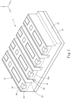
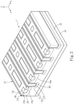
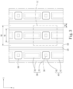
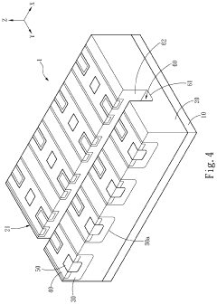
01 Package structures for SiC MOSFETs
Various package structures are designed specifically for SiC MOSFETs to optimize thermal performance and electrical characteristics. These packages include specialized layouts to handle the high temperature and high voltage capabilities of SiC devices. The package designs incorporate features such as improved heat dissipation paths, reduced parasitic inductance, and enhanced electrical isolation to maximize the performance advantages of SiC technology.- Package structure designs for SiC MOSFETs: Various package structure designs are employed for SiC MOSFETs to enhance thermal performance and reliability. These designs include specialized layouts for die attachment, lead frames, and encapsulation methods that accommodate the unique properties of silicon carbide. Advanced package structures help in managing the high temperature operation capabilities of SiC devices while maintaining electrical performance and mechanical stability.
- Thermal management solutions in SiC MOSFET packaging: Thermal management is critical in SiC MOSFET packaging due to the high power density and operating temperatures of these devices. Solutions include advanced heat sink designs, thermal interface materials, and cooling structures integrated into the package. These thermal management approaches help dissipate heat efficiently, prevent thermal runaway, and ensure reliable operation under high-power conditions.
- Interconnection techniques for SiC MOSFET modules: Specialized interconnection techniques are used in SiC MOSFET packaging to minimize parasitic inductance and resistance. These include advanced wire bonding methods, clip bonding, sintered connections, and direct copper bonding. Such techniques improve switching performance, reduce power losses, and enhance the overall efficiency of SiC MOSFET modules in high-frequency applications.
- Encapsulation materials for SiC MOSFET reliability: Specialized encapsulation materials are developed for SiC MOSFET packaging to withstand high operating temperatures and protect against environmental factors. These materials include advanced molding compounds, silicone gels, and ceramic-based encapsulants that offer superior thermal stability, moisture resistance, and electrical insulation properties, thereby extending the lifetime and reliability of SiC power devices.
- Multi-chip module integration for SiC power devices: Multi-chip module (MCM) integration approaches are employed in SiC MOSFET packaging to create compact, high-performance power modules. These designs integrate multiple SiC dies, gate drivers, protection circuits, and passive components within a single package. MCM solutions optimize power density, reduce parasitic effects, and enable more efficient power conversion systems for applications such as electric vehicles and industrial drives.
02 Thermal management solutions for SiC MOSFET packages
Thermal management is critical for SiC MOSFET packaging due to the high power density and operating temperatures of these devices. Advanced cooling solutions include direct liquid cooling, double-sided cooling structures, and specialized thermal interface materials. These solutions help to efficiently dissipate heat from the SiC die, allowing the device to operate at higher power levels while maintaining reliability and performance.Expand Specific Solutions03 Die attach materials and techniques for SiC MOSFETs
Specialized die attach materials and techniques are employed for SiC MOSFET packaging to ensure reliable operation at high temperatures. Silver sintering, high-temperature solders, and pressure-assisted bonding methods are used to create robust connections between the SiC die and package substrate. These materials and techniques provide superior thermal conductivity and mechanical stability compared to conventional die attach methods used for silicon devices.Expand Specific Solutions04 Wire bonding and interconnect technologies for SiC MOSFETs
Advanced interconnect technologies are developed for SiC MOSFET packaging to minimize parasitic inductance and resistance. These include heavy aluminum wire bonding, copper wire bonding, ribbon bonding, and clip bonding techniques. Some packages eliminate wire bonds entirely in favor of direct copper connections or embedded die technologies, which can significantly improve electrical performance and reliability under high-temperature cycling conditions.Expand Specific Solutions05 Module-level packaging for SiC MOSFETs
Module-level packaging solutions integrate multiple SiC MOSFETs into power modules designed for specific applications such as electric vehicles, renewable energy systems, and industrial drives. These modules feature optimized layouts for parallel operation, integrated gate drivers, current sensing, and protection circuits. Advanced module designs incorporate low-inductance bus structures, balanced current distribution, and efficient cooling to maximize the switching speed and power density advantages of SiC technology.Expand Specific Solutions
Key Industry Players in SiC MOSFET Packaging
The SiC MOSFET packaging market is currently in a growth phase, with increasing adoption across power electronics applications. The market is projected to expand significantly as industries transition from silicon to wide bandgap semiconductors for higher efficiency and performance. Key packaging challenges include thermal management, parasitic inductance reduction, and reliability under high-temperature operation. Companies like Infineon Technologies, Mitsubishi Electric, and TSMC are leading with advanced packaging solutions, while emerging players such as BASiC Semiconductor, Global Power Technology, and Shenzhen AST Technology are developing innovative approaches. Academic institutions including Hunan University and Xi'an Jiaotong University are contributing research to overcome reliability and cost barriers that currently limit wider SiC MOSFET adoption.
Mitsubishi Electric Corp.
Technical Solution: Mitsubishi Electric has developed a comprehensive SiC MOSFET packaging solution focused on addressing parasitic inductance and thermal challenges in high-power applications. Their approach utilizes direct lead bonding (DLB) technology that replaces traditional aluminum wire bonds with copper lead frames directly bonded to the semiconductor surface, reducing parasitic inductance by approximately 60%[1]. Mitsubishi's J-Series SiC modules feature an advanced direct copper bonding (DCB) substrate with optimized layout that reduces thermal resistance by up to 30% compared to conventional designs[2]. Their packaging incorporates specially formulated silicone gel encapsulation that maintains dielectric strength at high temperatures while accommodating the different thermal expansion coefficients of package materials. Additionally, Mitsubishi has pioneered a dual-sided cooling structure that enables heat extraction from both sides of the SiC chip, effectively doubling the cooling capacity in high-current applications[3].
Strengths: Exceptional reduction in parasitic inductance improving switching performance; superior thermal management through dual-sided cooling; high reliability under thermal cycling. Weaknesses: Higher production costs compared to conventional packaging; more complex manufacturing process requiring specialized equipment; larger physical footprint for some package designs.
BASiC Semiconductor Co., Ltd.
Technical Solution: BASiC Semiconductor has developed innovative packaging solutions for SiC MOSFETs that specifically address the challenges of high-temperature operation and parasitic inductance. Their proprietary packaging technology employs copper clip bonding instead of traditional aluminum wire bonds, reducing parasitic inductance by approximately 40% and enabling faster switching speeds with lower losses[1]. BASiC's thermal management approach incorporates direct copper bonding with specialized thermal interface materials that can withstand temperatures exceeding 200°C while maintaining thermal conductivity above 150 W/mK[2]. Their packages feature optimized internal layouts that minimize current crowding and distribute heat more evenly across the die surface. Additionally, BASiC has developed a novel encapsulation material specifically formulated for SiC applications that maintains dielectric strength at elevated temperatures while accommodating the thermal expansion mismatch between silicon carbide and packaging materials, significantly improving reliability during thermal cycling tests[3].
Strengths: Excellent thermal performance enabling operation at higher temperatures; reduced parasitic inductance improving switching characteristics; enhanced reliability under thermal cycling conditions. Weaknesses: Higher manufacturing complexity requiring specialized equipment; increased production costs compared to traditional packaging; limited availability in some package formats.
Critical Technologies in SiC Device Packaging
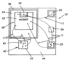
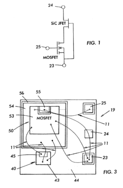
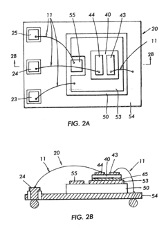
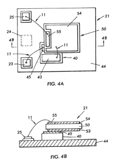
High power silicon carbide and silicon semiconductor device package
PatentInactiveUS6900537B2
Innovation
- A SiC-based field effect transistor (SiCFET) is co-packaged with a silicon MOSFET in a unitary structure, allowing electrode-on-electrode mounting for improved thermal management and reduced footprint, with the SiCFET providing faster switching and reduced thermal complexity.
Silicon carbide semiconductor device
PatentPendingUS20240234569A9
Innovation
- A silicon carbide semiconductor device with a hybrid gate structure featuring a trench gate configuration that reduces JFET resistance and parasitic gate-to-drain capacitance, enhancing switching performance by increasing channel width density and optimizing the layout of doped regions and trenches.
Thermal Management Strategies for SiC Devices
Thermal management is a critical aspect of SiC MOSFET packaging due to the high-temperature operation capabilities of silicon carbide devices. While SiC MOSFETs can theoretically operate at junction temperatures up to 600°C, current commercial packages typically limit operation to 175-200°C due to packaging material constraints. This temperature gap represents both a challenge and an opportunity for thermal management innovation.
Advanced thermal interface materials (TIMs) play a crucial role in SiC device packaging. Traditional solder-based TIMs are being replaced by silver sintering, which offers superior thermal conductivity (>200 W/mK compared to 50-60 W/mK for conventional solders) and higher melting points. These characteristics enable better heat dissipation and reliability at elevated temperatures typical in SiC applications.
Direct liquid cooling strategies are gaining prominence for high-power SiC modules. Two-phase cooling systems utilizing the latent heat of vaporization can achieve heat flux dissipation exceeding 500 W/cm², significantly outperforming traditional air cooling methods. Jet impingement and micro-channel cooling structures integrated directly into the device substrate have demonstrated thermal resistance reductions of up to 60% compared to conventional cooling methods.
Novel substrate materials are being developed specifically for SiC thermal management. Silicon nitride (Si₃N₄) and aluminum nitride (AlN) substrates offer thermal conductivities of 90-170 W/mK while maintaining electrical isolation properties. These advanced ceramic substrates can better match the coefficient of thermal expansion (CTE) of SiC, reducing thermomechanical stress during power cycling.
Double-sided cooling architectures represent another significant advancement, allowing heat extraction from both sides of the SiC die. This approach can potentially double the cooling capacity compared to single-sided solutions. Implementation requires specialized packaging techniques such as sandwich structures with dual cooling plates or embedded die technologies that expose both die surfaces to cooling media.
Computational fluid dynamics (CFD) modeling has become essential for optimizing thermal management solutions for SiC devices. These simulation tools enable designers to predict hotspots, optimize cooling channel geometries, and evaluate different cooling strategies before physical prototyping. Advanced thermal models that account for the unique properties of SiC, including its higher thermal conductivity and temperature-dependent characteristics, are being developed to improve prediction accuracy.
The integration of temperature sensors and active cooling control systems within SiC packages is emerging as a strategy to optimize thermal performance under varying operating conditions. These smart thermal management systems can adjust cooling parameters in real-time based on actual device temperatures, potentially extending device lifetime while maximizing performance.
Reliability Testing Standards for SiC Packages
Reliability testing standards for SiC packages have evolved significantly to address the unique challenges posed by silicon carbide power devices. These standards are crucial for ensuring that SiC MOSFET packages can withstand the harsh operating conditions they are designed for, including high temperatures, thermal cycling, and mechanical stress.
The Joint Electron Device Engineering Council (JEDEC) has established several standards specifically applicable to SiC device packaging. JEDEC JESD22-A104 outlines temperature cycling requirements, which for SiC packages often need to be extended beyond traditional silicon parameters to account for operating temperatures exceeding 200°C. Similarly, JEDEC JESD22-A108 addresses power cycling, a critical test for SiC MOSFETs that frequently operate in rapid switching applications.
Automotive Electronics Council (AEC) standards, particularly AEC-Q101 for discrete semiconductors, have been adapted for SiC devices with more stringent requirements. These modifications include extended high-temperature operating life (HTOL) tests at temperatures up to 175°C and beyond, reflecting the higher temperature capabilities of SiC technology.
IEC 60749 series standards provide comprehensive reliability testing methodologies that have been increasingly referenced for SiC package qualification. These include specific tests for moisture sensitivity levels (MSL), which are particularly important given the hermetic sealing challenges in SiC packaging.
Military standards such as MIL-STD-750 and MIL-STD-883 have also been adapted for SiC devices used in defense and aerospace applications, where reliability under extreme conditions is paramount. These standards incorporate specialized tests for radiation hardness and extended temperature range operation.
Industry-specific standards are emerging as SiC adoption increases across sectors. For example, power conversion applications often reference IEEE 1580 for electronic packaging, while automotive applications may follow LV 124 standards for electrical components in vehicles, with specific adaptations for SiC technology.
Testing methodologies for SiC packages must address unique failure modes not typically seen in silicon devices. These include die attach degradation at elevated temperatures, wire bond reliability under high current density conditions, and encapsulant breakdown under high electric fields. Consequently, accelerated life testing parameters often need recalibration for SiC devices, with acceleration factors adjusted to account for different activation energies and failure mechanisms.
As the industry matures, there is a growing consensus on the need for standardized reliability metrics specifically designed for SiC packaging technologies, moving beyond adapted silicon-based standards to truly address the unique characteristics and failure modes of SiC power devices.
Unlock deeper insights with Patsnap Eureka Quick Research — get a full tech report to explore trends and direct your research. Try now!
Generate Your Research Report Instantly with AI Agent
Supercharge your innovation with Patsnap Eureka AI Agent Platform!