

Gate Drive Design Considerations For SiC MOSFETs
SEP 5, 20259 MIN READ
Generate Your Research Report Instantly with AI Agent
PatSnap Eureka helps you evaluate technical feasibility & market potential.
SiC MOSFET Gate Drive Evolution and Objectives
Silicon Carbide (SiC) MOSFET technology has evolved significantly over the past two decades, transforming from a niche research area to a commercially viable alternative to traditional silicon-based power devices. The evolution of SiC MOSFET gate drive technology has been driven by the inherent material properties of SiC, which offers superior performance characteristics including higher breakdown voltage, faster switching speeds, and better thermal conductivity compared to silicon.
In the early 2000s, the first generation of SiC MOSFETs faced significant challenges related to gate oxide reliability and threshold voltage instability. Gate drive designs during this period were primarily focused on addressing these fundamental reliability issues rather than optimizing performance. The typical gate voltage ranges were conservative, often limited to +15V/-5V, to prevent premature device failure.
By the mid-2010s, second-generation SiC MOSFETs emerged with improved gate oxide quality and more stable threshold voltages. This advancement allowed gate drive designs to evolve toward higher switching frequencies and more efficient operation. During this phase, the industry began to recognize the need for specialized gate drivers specifically optimized for SiC characteristics rather than adapting silicon IGBT drivers.
The current generation of SiC MOSFETs, introduced around 2018-2020, features significantly enhanced ruggedness and reliability. Gate drive technology has correspondingly evolved to leverage these improvements, with a focus on maximizing switching performance while maintaining safe operation. Modern gate drivers now commonly incorporate advanced features such as programmable gate resistance, active Miller clamp functionality, and sophisticated protection mechanisms.
The primary objectives of contemporary SiC MOSFET gate drive design include minimizing switching losses, controlling dv/dt and di/dt rates to reduce electromagnetic interference (EMI), ensuring robust short-circuit protection, and maintaining long-term reliability under various operating conditions. These objectives must be balanced against practical considerations such as cost, complexity, and compatibility with existing systems.
Looking forward, the evolution of SiC MOSFET gate drives is expected to continue along several trajectories. Integration of advanced sensing and protection features directly into gate driver ICs represents one significant trend. Another is the development of intelligent gate drivers with adaptive control algorithms that can optimize switching parameters in real-time based on operating conditions. Additionally, there is growing interest in resonant gate drive topologies that can recover gate energy, particularly important for high-frequency applications where gate losses become significant.
The ultimate goal of this evolutionary path is to fully exploit the performance potential of SiC technology while ensuring reliability and cost-effectiveness across diverse application domains ranging from automotive traction inverters to renewable energy systems and industrial power supplies.
Market Demand Analysis for SiC Power Electronics
The Silicon Carbide (SiC) power electronics market is experiencing unprecedented growth, driven by the increasing demand for high-efficiency power conversion systems across multiple industries. Current market analysis indicates that the global SiC power device market is projected to grow at a compound annual growth rate of 29% through 2026, reaching a market value of $2.5 billion. This remarkable growth is primarily fueled by the superior properties of SiC MOSFETs compared to traditional silicon-based devices, including higher breakdown voltage, faster switching speeds, and better thermal conductivity.
The automotive sector represents the largest market segment for SiC power electronics, particularly in electric vehicle (EV) applications. The need for more efficient power conversion in EV powertrains is driving adoption, as SiC-based inverters can increase vehicle range by 5-10% compared to silicon alternatives. Major automotive manufacturers have already begun integrating SiC technology into their latest EV models, with projections indicating that over 60% of electric vehicles will utilize SiC power electronics by 2030.
Industrial applications constitute the second-largest market segment, with particular emphasis on motor drives, power supplies, and renewable energy systems. The industrial sector values SiC MOSFETs for their ability to operate at higher temperatures and frequencies, which enables smaller system footprints and reduced cooling requirements. Market research indicates that industrial SiC applications will grow at 32% annually through 2025.
The renewable energy sector presents another significant growth opportunity for SiC power electronics. Solar inverters utilizing SiC MOSFETs demonstrate efficiency improvements of 1-2% compared to silicon-based alternatives, which translates to substantial energy savings over system lifetimes. Wind power systems similarly benefit from SiC technology through improved power density and reliability in harsh operating environments.
Regional analysis reveals that Asia-Pacific currently dominates the SiC power electronics market, accounting for approximately 45% of global demand. This is largely attributed to the region's robust manufacturing base for automotive and consumer electronics. North America and Europe follow with market shares of 30% and 20% respectively, with both regions showing accelerated adoption rates in automotive and industrial applications.
Market challenges include the relatively high cost of SiC devices compared to silicon alternatives, with SiC MOSFETs typically commanding a 2-3x price premium. However, this gap is narrowing as manufacturing scales increase and yields improve. Additionally, the specialized gate drive requirements for SiC MOSFETs represent both a technical challenge and market opportunity, as optimized gate drive solutions are essential to fully realize the performance benefits of SiC technology.
Technical Challenges in SiC MOSFET Gate Drive Design
SiC MOSFETs present unique challenges for gate drive design that significantly differ from traditional silicon-based devices. The higher switching speeds and increased operating frequencies of SiC MOSFETs demand gate drivers with exceptional performance characteristics. One primary challenge is managing the significantly higher dv/dt and di/dt rates, which can reach 50-100 V/ns and 1-5 A/ns respectively, creating substantial electromagnetic interference (EMI) and potential false triggering issues.
The gate threshold voltage characteristics of SiC MOSFETs present another critical challenge. Unlike silicon devices, SiC MOSFETs typically have lower and less stable threshold voltages, making them more susceptible to noise-induced spurious turn-on events. This vulnerability is exacerbated by the Miller capacitance effect during high-speed switching, requiring sophisticated gate drive solutions to maintain switching integrity.
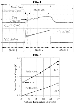
Thermal management represents a significant hurdle in SiC MOSFET gate drive design. The higher operating temperatures of SiC devices (potentially up to 200°C) necessitate gate drivers with enhanced thermal performance and reliability. Additionally, the temperature coefficient of the threshold voltage in SiC MOSFETs differs from silicon devices, requiring compensation mechanisms in the gate drive circuit to maintain consistent performance across temperature ranges.
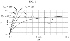
The optimal gate voltage requirements for SiC MOSFETs present another design challenge. While silicon MOSFETs typically operate with gate voltages of +15V/-5V, SiC MOSFETs often require +20V/-5V or even higher positive gate voltages to achieve optimal on-state resistance. However, these devices also have narrower gate voltage margins before breakdown, necessitating precise voltage control and protection mechanisms.
Short-circuit protection poses particular difficulties with SiC MOSFETs due to their reduced short-circuit withstand time (typically 1-2 μs compared to 10 μs for silicon devices). This requires ultra-fast detection and response circuits that can identify fault conditions and safely shut down the device before catastrophic failure occurs.
Layout and parasitic considerations become increasingly critical with SiC technology. The high switching speeds amplify the impact of parasitic inductances in the gate drive loop, potentially causing voltage overshoots, ringing, and switching losses. Gate drive designs must incorporate careful layout techniques, minimizing loop areas and utilizing specialized components like ferrite beads or common-mode chokes to mitigate these effects.
Isolation requirements are also more demanding for SiC MOSFET applications, particularly in high-voltage systems where common-mode transient immunity (CMTI) must exceed 100 kV/μs. This necessitates advanced isolation technologies such as reinforced galvanic isolation or optical isolation with superior performance characteristics.
The gate threshold voltage characteristics of SiC MOSFETs present another critical challenge. Unlike silicon devices, SiC MOSFETs typically have lower and less stable threshold voltages, making them more susceptible to noise-induced spurious turn-on events. This vulnerability is exacerbated by the Miller capacitance effect during high-speed switching, requiring sophisticated gate drive solutions to maintain switching integrity.
Thermal management represents a significant hurdle in SiC MOSFET gate drive design. The higher operating temperatures of SiC devices (potentially up to 200°C) necessitate gate drivers with enhanced thermal performance and reliability. Additionally, the temperature coefficient of the threshold voltage in SiC MOSFETs differs from silicon devices, requiring compensation mechanisms in the gate drive circuit to maintain consistent performance across temperature ranges.
The optimal gate voltage requirements for SiC MOSFETs present another design challenge. While silicon MOSFETs typically operate with gate voltages of +15V/-5V, SiC MOSFETs often require +20V/-5V or even higher positive gate voltages to achieve optimal on-state resistance. However, these devices also have narrower gate voltage margins before breakdown, necessitating precise voltage control and protection mechanisms.
Short-circuit protection poses particular difficulties with SiC MOSFETs due to their reduced short-circuit withstand time (typically 1-2 μs compared to 10 μs for silicon devices). This requires ultra-fast detection and response circuits that can identify fault conditions and safely shut down the device before catastrophic failure occurs.
Layout and parasitic considerations become increasingly critical with SiC technology. The high switching speeds amplify the impact of parasitic inductances in the gate drive loop, potentially causing voltage overshoots, ringing, and switching losses. Gate drive designs must incorporate careful layout techniques, minimizing loop areas and utilizing specialized components like ferrite beads or common-mode chokes to mitigate these effects.
Isolation requirements are also more demanding for SiC MOSFET applications, particularly in high-voltage systems where common-mode transient immunity (CMTI) must exceed 100 kV/μs. This necessitates advanced isolation technologies such as reinforced galvanic isolation or optical isolation with superior performance characteristics.
Current Gate Drive Solutions for SiC MOSFETs
01 Gate drive voltage and current considerations
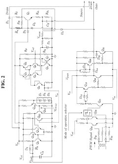
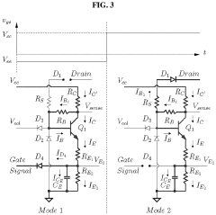
SiC MOSFETs require specific gate drive voltage and current parameters for optimal operation. The gate drive design must account for the higher threshold voltages compared to silicon MOSFETs, typically requiring a positive gate voltage of +15V to +20V for turn-on and a negative voltage of -2V to -5V for turn-off to prevent unwanted switching. Additionally, sufficient gate current is necessary to charge and discharge the gate capacitance quickly, reducing switching losses and ensuring proper operation at high frequencies.- Gate Drive Circuit Design for SiC MOSFETs: Specialized gate drive circuits are essential for SiC MOSFETs to handle their unique switching characteristics. These circuits typically include optimized gate resistors, voltage levels, and protection mechanisms to ensure reliable operation. The gate drive design must account for the higher switching speeds and gate voltage requirements of SiC devices compared to traditional silicon MOSFETs, while preventing parasitic turn-on and oscillations during high-speed switching events.
- Protection and Isolation Strategies: SiC MOSFET gate drives require robust protection mechanisms due to their sensitivity to overvoltage and overcurrent conditions. Isolation techniques such as optocouplers or digital isolators are implemented to separate control circuits from power stages. Advanced protection features include desaturation detection, short-circuit protection, and gate voltage monitoring to prevent device failure during fault conditions while maintaining the high-speed switching capability of SiC devices.
- Thermal Management Considerations: Effective thermal management is critical in SiC MOSFET gate drive designs due to the high power density and switching frequencies. Gate drive circuits must be designed to minimize power losses and heat generation while maintaining optimal switching performance. This includes considerations for component placement, heat sinking, and thermal interface materials to ensure reliable operation across a wide temperature range and prevent thermal runaway conditions.
- Parasitic Inductance Mitigation: Minimizing parasitic inductances is crucial in SiC MOSFET gate drive designs due to their fast switching speeds. Layout optimization techniques include compact PCB designs, minimized loop areas, and strategic component placement. Advanced gate drive topologies incorporate Kelvin source connections and optimized current paths to reduce common-source inductance, which helps prevent voltage overshoots, ringing, and false triggering during high-speed switching transitions.
- Multi-level and Advanced Gate Drive Techniques: Advanced gate drive techniques for SiC MOSFETs include multi-level gate driving, active gate driving, and resonant gate drive circuits. These approaches provide precise control over switching transitions, reducing switching losses and EMI while improving overall system efficiency. Adaptive gate drive methods can dynamically adjust gate voltage and current profiles based on operating conditions, optimizing the trade-off between switching speed and electromagnetic interference in high-frequency applications.
02 Protection circuits and isolation techniques
Protection circuits are essential in SiC MOSFET gate drive designs to prevent device failure due to overvoltage, overcurrent, or short-circuit conditions. These include desaturation detection, active Miller clamping, and soft turn-off mechanisms. Additionally, proper isolation between the control circuitry and power stage is critical, especially in high-voltage applications, to prevent noise coupling and ensure reliable operation. Optocouplers, digital isolators, or transformer-based isolation can be implemented to maintain signal integrity while providing the necessary voltage isolation.Expand Specific Solutions03 Layout and parasitic considerations
PCB layout is crucial for SiC MOSFET gate drive performance. Minimizing parasitic inductance in the gate drive loop is essential to prevent voltage oscillations and ensure clean switching transitions. This includes keeping gate drive traces short, using proper ground planes, and optimizing component placement. The gate resistor selection and placement also significantly impact switching behavior, with separate turn-on and turn-off resistors often used to independently control switching speeds and reduce electromagnetic interference while maintaining efficiency.Expand Specific Solutions04 Temperature and reliability considerations
SiC MOSFETs operate at higher temperatures than silicon devices, requiring gate drive designs that maintain performance across wide temperature ranges. This includes selecting components with appropriate temperature ratings and implementing temperature compensation techniques. The gate drive must also account for the reliability challenges specific to SiC MOSFETs, such as threshold voltage shifts over time and increased susceptibility to gate oxide breakdown. Robust design practices include implementing appropriate safety margins in voltage ratings and incorporating monitoring circuits for long-term reliability.Expand Specific Solutions05 Advanced gate drive topologies
Advanced gate drive topologies enhance SiC MOSFET performance beyond conventional designs. These include resonant gate drivers that recover gate energy to improve efficiency, multi-level gate drivers that provide different voltage levels during switching transitions to optimize the trade-off between switching losses and EMI, and intelligent gate drivers with integrated protection features and adaptive control capabilities. These advanced topologies often incorporate digital control elements to dynamically adjust gate drive parameters based on operating conditions, further optimizing system performance.Expand Specific Solutions
Key Industry Players in SiC MOSFET Ecosystem
The SiC MOSFET gate drive design market is in a growth phase, with increasing adoption across power electronics applications due to superior performance over traditional silicon devices. The global market is expanding rapidly, driven by electric vehicle adoption, renewable energy integration, and industrial automation. Leading players include established semiconductor manufacturers like Wolfspeed, Infineon Technologies, and Microchip Technology, who have developed mature gate drive solutions. Chinese companies such as BASiC Semiconductor and Global Power Technology are emerging as significant competitors. Academic-industry collaborations involving institutions like Xidian University and University of Electronic Science & Technology of China are accelerating innovation. The technology has reached commercial maturity for lower voltage applications, while higher voltage solutions continue to evolve with ongoing R&D from major players to address thermal management and reliability challenges.
General Electric Company
Technical Solution: General Electric has developed sophisticated gate drive solutions for SiC MOSFETs focused on high-power industrial and renewable energy applications. Their approach centers on robust isolation technology using fiber optic interfaces that provide superior common-mode noise immunity (>200kV/μs) and isolation voltage ratings exceeding 20kV. GE's gate drivers implement precise voltage regulation maintaining +20V/-5V levels with less than 2% variation even under high switching frequencies up to 100kHz. Their designs incorporate advanced Active Gate Control (AGC) technology that dynamically adjusts gate resistance during switching transitions, with separate paths for turn-on and turn-off that can be independently optimized. This allows precise control of dv/dt rates between 10-40V/ns while minimizing switching losses. GE's gate drivers feature sophisticated thermal management techniques including integrated temperature sensors with ±2°C accuracy and dynamic derating capabilities that adjust switching parameters based on junction temperature estimates. Their protection architecture implements a hierarchical approach with multiple detection mechanisms for overcurrent, overvoltage, and thermal events, featuring response times under 500ns and programmable fault handling strategies. Additionally, GE has developed specialized gate drive power supply solutions that maintain stable operation even during grid disturbances, with hold-up times exceeding 100ms to ensure continuous protection during transient events.
Strengths: Exceptional isolation performance suitable for medium voltage applications; robust design for harsh industrial environments; advanced thermal management capabilities for high-reliability applications. Weaknesses: Larger physical footprint compared to integrated solutions; higher cost structure reflecting industrial-grade components; more complex implementation requiring specialized knowledge.
Infineon Technologies AG
Technical Solution: Infineon has developed advanced gate drive solutions specifically optimized for SiC MOSFETs, focusing on addressing the unique challenges these devices present. Their CoolSiC™ MOSFET gate driver designs incorporate precise voltage control mechanisms that maintain optimal gate voltage levels (typically +15V/-5V) to ensure proper device operation while preventing gate oxide damage. Infineon's gate drivers feature ultra-fast switching capability with rise/fall times under 10ns and propagation delays less than 50ns to fully leverage SiC's high-speed switching potential. Their designs include sophisticated dv/dt control circuits that can be adjusted between 5-50V/ns to balance switching losses and EMI. Additionally, Infineon has implemented advanced short-circuit protection with response times under 1μs and integrated temperature compensation to maintain consistent performance across operating conditions. Their gate drivers also feature galvanic isolation rated up to 1500V with high common-mode transient immunity (CMTI) exceeding 100kV/μs to ensure reliable operation in high-power applications.
Strengths: Industry-leading isolation technology with exceptional CMTI performance; comprehensive protection features including desaturation detection and soft shutdown capabilities; highly optimized driver solutions specifically matched to their SiC MOSFET portfolio. Weaknesses: Premium pricing compared to generic solutions; some designs require additional external components for full functionality; proprietary features may limit interoperability with third-party SiC devices.
Critical Patents and Innovations in SiC Gate Drive Circuits
High temperature gate driver for silicon carbide metal-oxide-semiconductor field-effect transistor
PatentActiveUS11218145B2
Innovation
- A low-cost high temperature gate driver utilizing commercial-off-the-shelf discrete transistors and diodes, integrated with a robust overcurrent and under voltage lock out protection circuit, capable of operating up to 180°C, featuring a reduced propagation delay and flexible short-circuit protection, designed to minimize self-heating and enhance reliability.
Silicon carbide semiconductor device
PatentPendingUS20240234569A9
Innovation
- A silicon carbide semiconductor device with a hybrid gate structure featuring a trench gate configuration that reduces JFET resistance and parasitic gate-to-drain capacitance, enhancing switching performance by increasing channel width density and optimizing the layout of doped regions and trenches.
Thermal Management Considerations for SiC Gate Drivers
Thermal management is a critical aspect of SiC MOSFET gate driver design due to the high switching frequencies and temperatures these devices operate at. SiC MOSFETs can function efficiently at junction temperatures up to 200°C, significantly higher than traditional silicon devices. This thermal capability creates unique challenges for gate driver circuits that must maintain reliable operation in these extreme conditions.
Gate drivers for SiC MOSFETs generate considerable heat during high-frequency switching operations, primarily due to the charging and discharging of the gate capacitance. The power dissipation in the gate driver increases linearly with switching frequency, making thermal management increasingly important as frequencies push beyond 100 kHz in modern applications.
The thermal interface between the gate driver IC and the PCB requires careful consideration. Advanced thermal vias, copper pour techniques, and specialized thermal interface materials can significantly improve heat dissipation. Multi-layer PCBs with dedicated thermal layers have become standard practice for high-performance SiC applications to efficiently channel heat away from sensitive components.
Isolation components in gate driver circuits present particular thermal challenges. Optocouplers and digital isolators, essential for maintaining isolation between control and power circuits, often have limited temperature ratings that can become bottlenecks in the thermal design. Next-generation silicon carbide gate drivers increasingly incorporate isolators rated for extended temperature ranges to address this limitation.
Active cooling solutions may be necessary for high-power density applications. While passive cooling through heatsinks and thermal vias is preferred for reliability, some cutting-edge designs incorporate miniature fans or liquid cooling systems integrated directly with the gate driver circuitry to maintain optimal operating temperatures.
Temperature monitoring and protection features are increasingly being integrated into advanced gate driver designs. These include thermal sensors and shutdown circuits that can detect overtemperature conditions and take protective actions before damage occurs. Some sophisticated gate drivers now incorporate dynamic thermal management algorithms that adjust switching parameters based on temperature feedback.
The physical placement of gate drivers relative to power devices requires careful thermal planning. While electrical considerations often dictate placing gate drivers as close as possible to SiC MOSFETs to minimize parasitic inductance, this proximity can create thermal coupling issues. Advanced designs often incorporate thermal barriers or strategic component placement to balance these competing requirements.
EMI/EMC Challenges and Mitigation Strategies
Silicon Carbide (SiC) MOSFETs, while offering superior performance characteristics, present significant EMI/EMC challenges that must be addressed in gate drive design. The high switching speeds (dv/dt and di/dt) inherent to SiC devices generate substantial electromagnetic interference that can compromise system reliability and regulatory compliance. These rapid transitions create both conducted and radiated emissions across a broad frequency spectrum, typically extending into hundreds of megahertz.
The primary EMI/EMC challenges in SiC MOSFET gate drive design include common-mode noise generation, ground bounce effects, and parasitic oscillations. Common-mode noise arises from the displacement current through parasitic capacitances between switching nodes and ground, exacerbated by SiC's fast switching transitions. Ground bounce occurs when high di/dt flows through ground impedances, creating voltage differentials that can disrupt sensitive control circuitry. Parasitic oscillations emerge from the interaction between device capacitances and circuit inductances, particularly problematic in SiC applications due to higher switching frequencies.
Effective mitigation strategies begin with optimized PCB layout techniques. These include minimizing gate loop inductance through compact design, implementing separate power and signal grounds with strategic connection points, and utilizing ground planes to reduce common-mode paths. The physical separation of sensitive signal traces from high dv/dt nodes is essential, as is the careful routing of gate drive signals to minimize coupling.
Component selection plays a crucial role in EMI/EMC management. Gate resistors with appropriate values can control switching speeds, balancing EMI reduction against switching losses. Ferrite beads and common-mode chokes strategically placed in gate drive circuits help attenuate high-frequency noise. Snubber circuits, when properly designed, can dampen parasitic oscillations without significantly impacting efficiency.
Advanced shielding techniques provide additional protection, including local shielding of gate drive circuits and the implementation of Faraday shields between power and control sections. The careful selection of EMI filters at both input and output stages helps contain emissions within regulatory limits.
Measurement and verification form the final component of a comprehensive EMI/EMC strategy. Near-field probing can identify specific emission sources, while conducted EMI measurements verify compliance with standards such as CISPR 22 or FCC Part 15. System-level EMC testing under various operating conditions ensures robust performance in real-world applications.
Unlock deeper insights with PatSnap Eureka Quick Research — get a full tech report to explore trends and direct your research. Try now!
Generate Your Research Report Instantly with AI Agent
Supercharge your innovation with PatSnap Eureka AI Agent Platform!