How Do SiC MOSFETs Enable Smaller And Lighter Power Systems?
SEP 8, 20259 MIN READ
Generate Your Research Report Instantly with AI Agent
Patsnap Eureka helps you evaluate technical feasibility & market potential.
SiC MOSFET Technology Evolution and Objectives
Silicon Carbide (SiC) MOSFET technology represents a revolutionary advancement in power electronics, evolving significantly since its initial development in the early 1990s. The journey began with rudimentary devices plagued by reliability issues and high manufacturing costs, limiting their practical applications. By the early 2000s, researchers had made substantial progress in addressing the oxide interface quality challenges that had previously hindered SiC MOSFET performance.
The technology evolution accelerated around 2010 when companies like Cree (now Wolfspeed), ROHM, and STMicroelectronics began commercializing SiC MOSFETs with improved characteristics. This period marked a critical transition from laboratory research to industrial production, establishing SiC as a viable alternative to traditional silicon-based power devices.
A significant milestone occurred in 2011 when Toyota announced the incorporation of SiC power semiconductors in their hybrid vehicles, demonstrating the technology's potential in automotive applications. This industry adoption catalyzed further development, leading to enhanced device reliability and reduced production costs through economies of scale.
The evolution trajectory has been characterized by continuous improvements in key performance parameters. Early SiC MOSFETs operated at blocking voltages of 600-1200V, while modern devices can handle 1700V and beyond. Similarly, on-resistance values have decreased dramatically, with current devices achieving specific on-resistance figures approaching theoretical material limits.
Manufacturing processes have evolved from 4-inch wafers to 6-inch and now 8-inch platforms, significantly reducing per-unit costs and enabling broader market penetration. Concurrently, packaging technologies have advanced to maximize the inherent benefits of SiC, with innovations in thermal management and parasitic inductance reduction.
The primary objective of SiC MOSFET technology development has been to enable more efficient, compact, and lightweight power conversion systems across multiple industries. Specific goals include achieving higher switching frequencies (>100 kHz) while maintaining efficiency, enabling operation at elevated temperatures (>200°C), and reducing system-level cooling requirements.
Additional objectives encompass improving long-term reliability under harsh operating conditions, reducing device cost to approach silicon alternatives, and developing optimized gate driver solutions that address the unique switching characteristics of SiC. The technology aims to facilitate the miniaturization of power electronics in electric vehicles, renewable energy systems, industrial drives, and aerospace applications.
Looking forward, the technology roadmap focuses on further enhancing power density capabilities, with targets to exceed 100 W/cm³ at the system level while maintaining high efficiency across varying load conditions. This evolution continues to drive the transformation toward smaller, lighter, and more efficient power systems that can meet the demands of emerging applications in electrification and renewable energy integration.
Market Demand for Compact Power Systems
The global market for compact power systems is experiencing unprecedented growth, driven by the increasing demand for miniaturization across multiple industries. This trend is particularly evident in electric vehicles (EVs), renewable energy systems, industrial automation, and consumer electronics sectors. The EV market alone is projected to grow at a CAGR of 21.7% through 2030, with a significant emphasis on reducing the size and weight of power conversion systems to extend vehicle range and improve efficiency.
In the renewable energy sector, the shift toward distributed generation systems has intensified the need for compact, high-efficiency power electronics. Solar inverters and wind power converters are becoming increasingly compact to reduce installation costs and improve deployment flexibility, with the market for these systems expanding at approximately 15% annually.
Aerospace and defense applications represent another critical market segment demanding smaller and lighter power systems. Weight reduction directly translates to fuel savings and increased payload capacity, with each pound of weight reduction valued at thousands of dollars over an aircraft's lifetime. Military applications particularly benefit from SiC-based compact power systems due to their reliability under extreme conditions and reduced cooling requirements.
Data centers and telecommunications infrastructure are experiencing explosive growth in power density requirements. The global data center power market is expanding rapidly as operators seek to maximize computing power while minimizing facility footprint. Compact power systems enable higher rack densities and improved energy efficiency, addressing both space constraints and operational costs.
Consumer electronics manufacturers continue to push the boundaries of device miniaturization while increasing functionality. Fast chargers for mobile devices have decreased in size by over 40% in recent years while delivering higher power outputs, directly enabled by wide-bandgap semiconductor technologies like SiC MOSFETs.
Industrial automation systems benefit significantly from compact power electronics through reduced cabinet sizes, simplified thermal management, and increased reliability. The industrial power electronics market is growing steadily as manufacturers adopt more sophisticated motor drives and power conversion systems that occupy less factory floor space.
Transportation electrification extends beyond passenger vehicles to include commercial fleets, marine applications, and railway systems. Each of these segments requires power electronics that maximize space utilization while delivering exceptional performance under demanding operational conditions.
The market demand for compact power systems is further accelerated by regulatory pressures for improved energy efficiency and reduced environmental impact. Energy efficiency standards worldwide are becoming increasingly stringent, driving adoption of advanced power semiconductor technologies that enable smaller form factors without compromising performance.
Current SiC MOSFET Capabilities and Limitations
Silicon Carbide (SiC) MOSFETs have emerged as revolutionary components in power electronics, offering significant advantages over traditional silicon-based devices. Current SiC MOSFETs demonstrate exceptional capabilities in high-voltage applications, typically operating efficiently in the 650V to 1700V range, with some devices now reaching 3300V and beyond. These devices exhibit remarkably low on-resistance (RDS(on)) values that remain relatively stable across temperature variations, a critical advantage over silicon counterparts whose resistance increases dramatically at elevated temperatures.
The switching performance of modern SiC MOSFETs is particularly impressive, with switching frequencies commonly reaching 100-200 kHz in practical applications, compared to silicon IGBTs typically limited to 20-30 kHz. This high-frequency operation directly enables the reduction in passive component sizes, particularly inductors and capacitors, which constitute a significant portion of power system volume and weight.
Thermal performance represents another area where SiC MOSFETs excel, with junction temperature ratings typically reaching 175°C to 200°C, compared to 150°C for silicon devices. This superior thermal capability allows for reduced cooling requirements or higher power density within the same thermal management system. The material's wider bandgap (3.26 eV versus silicon's 1.12 eV) contributes to lower leakage currents and better high-temperature stability.
Despite these impressive capabilities, SiC MOSFETs still face several limitations. Cost remains a significant barrier, with SiC devices typically commanding a 2-3x price premium over silicon alternatives, though this gap continues to narrow as manufacturing volumes increase. Gate oxide reliability presents ongoing challenges, as the interface between SiC and SiO2 contains more defects than silicon-based interfaces, potentially affecting long-term device stability.
Channel mobility in SiC MOSFETs remains lower than in silicon devices, contributing to higher specific on-resistance for a given voltage rating. This limitation is gradually being addressed through improved manufacturing processes and device structures. Additionally, SiC MOSFETs exhibit more complex driving requirements, often necessitating careful gate driver design with appropriate voltage levels (typically +15V/-5V or +20V/-5V) to ensure optimal switching performance while preventing parasitic turn-on events.
Packaging technology represents another limitation, as traditional packaging struggles to fully leverage SiC's high-temperature and high-frequency capabilities. Advanced packaging solutions incorporating improved thermal management and reduced parasitic inductance are being developed but are not yet universally adopted.
The body diode performance in SiC MOSFETs, while improving, still presents challenges with higher forward voltage drop and slower reverse recovery compared to discrete SiC Schottky diodes, sometimes necessitating external diodes in certain applications where freewheeling performance is critical.
Technical Solutions for Size and Weight Reduction
01 Miniaturization of SiC MOSFETs
Silicon carbide (SiC) MOSFETs can be designed with reduced size and weight through advanced fabrication techniques. These techniques include optimized cell structures, improved lithography processes, and innovative packaging methods that allow for higher power density in smaller form factors. The miniaturization of SiC MOSFETs enables their integration into compact power electronic systems while maintaining high performance characteristics.- Compact SiC MOSFET designs for size reduction: Silicon carbide MOSFETs can be designed with compact structures to significantly reduce device size and weight compared to traditional silicon-based MOSFETs. These designs incorporate optimized cell structures, reduced gate dimensions, and efficient layout techniques that minimize the overall footprint while maintaining high performance characteristics. The compact designs enable higher power density in applications where space constraints are critical.
- Integration techniques for SiC MOSFETs in power modules: Advanced integration techniques allow SiC MOSFETs to be incorporated into power modules with reduced size and weight. These techniques include multi-chip packaging, 3D integration, and novel interconnect methods that optimize thermal management while minimizing the overall module dimensions. The integration approaches enable higher power handling capability in smaller form factors, making them suitable for weight-sensitive applications like electric vehicles and aerospace systems.
- Lightweight packaging solutions for SiC MOSFETs: Specialized packaging solutions for SiC MOSFETs focus on reducing weight while maintaining thermal performance and reliability. These include advanced materials such as lightweight composites, ceramic substrates, and optimized heat spreaders that reduce the overall weight of the package. The lightweight packaging solutions address thermal management challenges while contributing to overall system weight reduction in applications where power-to-weight ratio is critical.
- Miniaturization techniques for SiC MOSFET structures: Miniaturization techniques for SiC MOSFETs involve advanced fabrication processes that enable smaller device geometries while maintaining electrical performance. These techniques include refined lithography processes, optimized doping profiles, and innovative channel designs that allow for reduced die size. The miniaturized structures contribute to both size and weight reduction while potentially improving switching performance and thermal characteristics.
- Weight optimization through material selection in SiC MOSFETs: Material selection plays a crucial role in optimizing the weight of SiC MOSFETs. By utilizing advanced substrate materials, thinner wafers, and optimized metallization layers, the overall weight of the devices can be reduced. Additionally, the use of alternative bonding materials and connection techniques contributes to weight reduction while maintaining electrical and thermal performance. These material innovations enable lighter power electronic systems without compromising reliability.
02 Lightweight packaging solutions for SiC MOSFETs
Specialized packaging technologies have been developed to reduce the weight of SiC MOSFET modules. These include advanced materials such as lightweight composites, aluminum-based heat sinks, and thin-film substrates that provide effective thermal management while minimizing overall weight. Such packaging innovations are particularly important for applications where weight is a critical factor, such as in aerospace and automotive systems.Expand Specific Solutions03 Size optimization through vertical device structures
Vertical device architectures for SiC MOSFETs enable significant size reduction compared to traditional planar designs. By utilizing the vertical dimension, these structures achieve higher current densities and voltage ratings within a smaller footprint. The vertical configuration allows for more efficient use of semiconductor material and reduces the overall size and weight of the device while maintaining or improving electrical performance characteristics.Expand Specific Solutions04 Integration techniques for compact SiC MOSFET modules
Advanced integration techniques combine multiple SiC MOSFETs and associated components into compact modules. These techniques include multi-chip module approaches, 3D integration, and system-in-package solutions that minimize interconnection losses and reduce the overall footprint. Such integration methods enable the development of lightweight power modules with high power density, suitable for space-constrained applications.Expand Specific Solutions05 Thermal management for size-optimized SiC MOSFETs
Innovative thermal management solutions allow SiC MOSFETs to operate reliably in smaller packages. These include advanced cooling techniques such as direct liquid cooling, phase-change materials, and optimized heat spreader designs that efficiently dissipate heat from compact devices. Effective thermal management is crucial for maintaining performance and reliability while reducing the size and weight of SiC MOSFET-based power systems.Expand Specific Solutions
Leading SiC MOSFET Manufacturers and Competitors
The SiC MOSFET market is experiencing rapid growth in the power electronics industry, currently transitioning from early adoption to mainstream implementation. The global market is expanding significantly, driven by demands for higher efficiency and smaller power systems across automotive, industrial, and renewable energy sectors. From a technological maturity perspective, leading players like Infineon Technologies, Mitsubishi Electric, and Toshiba have established commercial product lines with advanced performance metrics, while newer entrants such as Huawei Digital Power and Fast SiC Semiconductor are accelerating innovation. Academic institutions including University of Electronic Science & Technology of China and Xi'an Jiaotong University are contributing fundamental research to overcome remaining challenges in device reliability and cost reduction, creating a competitive landscape where established semiconductor manufacturers compete with specialized SiC-focused startups.
Fast Sic Semiconductor, Inc.
Technical Solution: Fast SiC Semiconductor has developed innovative SiC MOSFET technology focused on ultra-fast switching performance. Their devices feature a proprietary trench-assisted planar gate structure that reduces internal gate resistance by approximately 40% compared to conventional designs. This enables switching transition times below 10ns while maintaining robust short-circuit capability exceeding 5μs. Fast SiC's MOSFETs incorporate specialized channel engineering that achieves threshold voltage stability across temperature ranges from -55°C to 175°C, with variation less than 200mV. Their technology utilizes advanced epitaxial growth processes that reduce defect density to below 1cm⁻² in the drift region, enabling higher yield and reliability. Fast SiC has also developed specialized packaging with reduced parasitic inductance (<2nH) that preserves the intrinsic switching speed advantages of their die technology.
Strengths: Industry-leading switching speed enabling highest frequency operation; specialized focus on SiC technology allows rapid innovation; devices optimized specifically for hard-switching applications. Weaknesses: Smaller manufacturing scale compared to major IDMs; more limited product portfolio breadth; newer entrant with less established reliability track record.
Mitsubishi Electric Corp.
Technical Solution: Mitsubishi Electric has developed advanced SiC MOSFET technology featuring their proprietary DMOS (Double-diffused MOS) structure with optimized cell pitch design. Their 2nd generation SiC MOSFETs achieve specific on-resistance values below 3.0mΩ·cm² while maintaining blocking voltages up to 1700V. Mitsubishi's devices incorporate specialized field limiting rings and junction termination extension structures that maximize breakdown voltage while minimizing chip area by approximately 25%. Their SiC modules feature direct liquid cooling technology that reduces thermal resistance by up to 40% compared to conventional air-cooled designs. This enables power density improvements exceeding 60% in traction applications. Mitsubishi has also developed specialized gate driver ICs with active Miller clamp functionality and short-circuit protection specifically optimized for their SiC devices, enabling reliable operation at switching frequencies up to 80kHz.
Strengths: Extensive experience in high-power applications like railway traction; advanced packaging technology for high-temperature operation; comprehensive module portfolio with integrated cooling solutions. Weaknesses: Higher cost structure than some competitors; more focused on high-power modules than discrete components; requires specialized gate drive circuitry for optimal performance.
Key SiC MOSFET Innovations and Patents
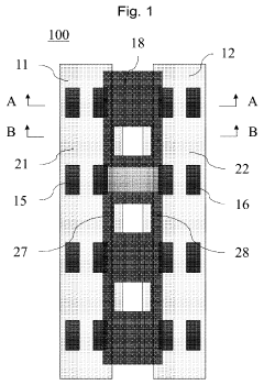
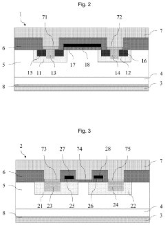
Silicon carbide power mos field effect transistors and manufacturing methods
PatentInactiveEP1576672A2
Innovation
- The implementation of an n-type silicon carbide limiting region with a higher carrier concentration than the drift layer, positioned between the drift layer and the p-type silicon carbide region, reduces the depletion region and on-state resistance by creating a shorter current path, and the use of an epitaxial layer or implanted regions to define the limiting region.
Silicon carbide metal oxide semiconductor field effect transistor and manufacturing method of silicon carbide metal oxide semiconductor field effect transistor
PatentPendingUS20230378341A1
Innovation
- The design incorporates alternating cells with specific well regions, source regions, and contact layers, including ohmic and Schottky contacts, to reduce channel density, enhance short-circuit tolerance, and minimize reverse leakage current and forward voltage drop, while maintaining the transistor's size and functionality.
Thermal Management Strategies for SiC Devices
Silicon Carbide (SiC) MOSFETs operate at significantly higher temperatures than their silicon counterparts, with junction temperatures reaching up to 200°C compared to silicon's typical 150°C limit. This thermal advantage enables more compact power system designs but simultaneously demands sophisticated thermal management strategies to ensure optimal performance and reliability.
Effective thermal management for SiC devices begins with proper package selection. Advanced packages like Direct Bonded Copper (DBC) substrates and double-sided cooling configurations maximize heat dissipation pathways. These packages feature reduced thermal resistance and improved thermal conductivity, allowing for more efficient heat transfer from the semiconductor die to the external environment.
Heat sink design represents another critical aspect of SiC thermal management. Traditional aluminum heat sinks are increasingly being replaced by copper or advanced composite materials with superior thermal conductivity. Optimized fin structures and increased surface area designs specifically engineered for SiC's thermal profile help maintain junction temperatures within safe operating limits while minimizing overall system size.
Active cooling solutions have evolved to address SiC's unique thermal characteristics. Forced-air cooling systems with high-efficiency fans and optimized airflow patterns provide enhanced cooling performance in compact spaces. For higher power densities, liquid cooling systems utilizing advanced coolants and microchannel structures offer superior thermal performance, enabling further size reduction of power conversion systems.
Thermal interface materials (TIMs) play a crucial role in SiC device cooling. Next-generation TIMs including phase-change materials, metal-based composites, and graphene-enhanced compounds offer significantly lower thermal resistance than conventional materials. These advanced TIMs minimize the thermal bottleneck between the SiC device and cooling system, allowing for more compact thermal solutions.
System-level thermal design considerations are equally important for SiC implementations. Computational fluid dynamics (CFD) modeling enables precise thermal simulation and optimization before physical prototyping. Strategic component placement to minimize thermal coupling between heat-generating elements and temperature-sensitive components further enhances system reliability while reducing overall size requirements.
Innovative cooling approaches specifically tailored for SiC applications continue to emerge. These include two-phase cooling systems, jet impingement cooling, and embedded cooling channels that provide exceptional thermal performance in extremely compact form factors. Such advanced cooling technologies are instrumental in fully leveraging SiC's potential to create smaller and lighter power systems while maintaining optimal operating temperatures.
Cost-Performance Analysis of SiC Implementation
The implementation of Silicon Carbide (SiC) MOSFETs in power systems represents a significant investment decision that must be evaluated through comprehensive cost-performance analysis. Initial acquisition costs of SiC components typically range 2-3 times higher than traditional silicon alternatives, creating an immediate barrier to adoption for cost-sensitive applications. However, this analysis must extend beyond purchase price to capture the total cost of ownership across the system lifecycle.
When evaluating system-level economics, SiC implementations demonstrate compelling advantages through reduced component count. The higher switching frequencies enabled by SiC allow for smaller passive components, particularly magnetic elements and capacitors, which can reduce overall bill of materials costs by 15-30% depending on application requirements. This consolidation effect cascades throughout the design, reducing PCB size, enclosure dimensions, and assembly complexity.
Energy efficiency improvements represent another critical economic factor. SiC-based systems typically achieve 98-99% efficiency compared to 94-96% for silicon equivalents, translating to significant operational cost savings. In high-power industrial applications operating continuously, these efficiency gains can offset the initial cost premium within 1-2 years through reduced energy consumption alone. For electric vehicles, the improved efficiency directly contributes to extended range capabilities without increasing battery capacity.
Thermal management costs decrease substantially with SiC implementation. The reduced cooling requirements allow for smaller heatsinks, simpler thermal designs, and in some cases, elimination of forced-air cooling systems. This reduction in thermal management infrastructure can represent 10-25% cost savings in system packaging while simultaneously improving reliability metrics through lower operating temperatures.
Reliability improvements further enhance the economic proposition. SiC devices demonstrate superior robustness under thermal cycling, voltage stress, and long-term operation. Mean Time Between Failures (MTBF) improvements of 30-50% compared to silicon alternatives translate to reduced warranty costs and maintenance expenses, particularly valuable in applications where downtime carries significant economic penalties.
Manufacturing considerations must also factor into the analysis. While SiC wafer production costs continue to decline through economies of scale and process refinements, they remain higher than silicon manufacturing. However, the system-level benefits in terms of reduced component count, simplified assembly, and improved yield rates increasingly offset these material cost premiums, particularly as production volumes increase.
Unlock deeper insights with Patsnap Eureka Quick Research — get a full tech report to explore trends and direct your research. Try now!
Generate Your Research Report Instantly with AI Agent
Supercharge your innovation with Patsnap Eureka AI Agent Platform!