

SiC MOSFET Modeling For Accurate Circuit Simulation
SEP 5, 20259 MIN READ
Generate Your Research Report Instantly with AI Agent
PatSnap Eureka helps you evaluate technical feasibility & market potential.
SiC MOSFET Evolution and Research Objectives
Silicon Carbide (SiC) MOSFET technology has undergone significant evolution since its initial development in the early 1990s. The journey began with rudimentary devices exhibiting high on-resistance and reliability issues, primarily confined to research laboratories. By the early 2000s, commercial viability started to emerge as manufacturers like Cree (now Wolfspeed) and Rohm introduced the first generation of SiC MOSFETs with improved performance characteristics, though still limited by high costs and manufacturing challenges.
The period from 2010 to 2015 marked a crucial transition phase, with substantial improvements in device performance, reliability, and cost reduction. During this time, SiC MOSFETs began penetrating high-end applications in aerospace, military, and industrial power conversion systems where their superior properties justified the premium cost.
From 2016 onwards, we have witnessed accelerated adoption across broader market segments, particularly in electric vehicles, renewable energy systems, and high-efficiency power supplies. This expansion has been driven by significant advancements in manufacturing processes, resulting in higher yields, lower defect densities, and reduced production costs.
Current state-of-the-art SiC MOSFETs feature blocking voltages ranging from 650V to 1700V, with specific on-resistance values approaching theoretical material limits. The latest generations demonstrate enhanced gate oxide reliability, improved threshold voltage stability, and reduced parasitic capacitances, enabling switching frequencies exceeding 100 kHz in practical applications.
Despite these advancements, accurate modeling of SiC MOSFETs remains a significant challenge for circuit designers. Traditional silicon-based MOSFET models fail to capture the unique physical characteristics of SiC devices, including their temperature-dependent behavior, non-linear capacitances, and body diode recovery characteristics.
The primary research objective in SiC MOSFET modeling is to develop comprehensive, physics-based models that accurately represent device behavior across all operating conditions while maintaining computational efficiency for circuit simulation environments. These models must capture static characteristics (forward conduction, blocking), dynamic switching behavior, and thermal dependencies with high fidelity.
Additional research goals include developing standardized parameter extraction methodologies to ensure model consistency across different device manufacturers and technology generations. Furthermore, there is a pressing need for models that can accurately predict device aging and reliability over extended operational lifetimes, particularly under high-temperature and high-switching frequency conditions typical in SiC applications.
The ultimate aim is to enable circuit designers to fully leverage SiC MOSFET capabilities through simulation tools that provide accurate predictions of efficiency, electromagnetic interference, thermal performance, and reliability before physical prototyping, thereby accelerating the adoption of this transformative technology across the power electronics industry.
Market Analysis for SiC Power Electronics
The Silicon Carbide (SiC) power electronics market has experienced remarkable growth in recent years, driven by increasing demand for high-efficiency power conversion systems across multiple industries. The global SiC power device market reached approximately $1.1 billion in 2022 and is projected to grow at a compound annual growth rate (CAGR) of 34% through 2028, potentially reaching $6.5 billion by the end of the forecast period.
Key market segments demonstrating strong demand include electric vehicles (EVs), renewable energy systems, industrial motor drives, and power supply units. The EV sector represents the largest and fastest-growing application segment, accounting for nearly 60% of the total SiC power electronics market. This dominance stems from automotive manufacturers' aggressive adoption of SiC technology to extend vehicle range, reduce charging times, and decrease overall system size and weight.
The renewable energy sector constitutes the second-largest market segment, with SiC devices increasingly deployed in solar inverters and wind power systems. Implementation of SiC MOSFETs in these applications has demonstrated efficiency improvements of 2-3% compared to traditional silicon-based solutions, translating to significant energy savings at utility scale.
Regional analysis reveals Asia-Pacific as the dominant market, representing approximately 45% of global SiC power electronics consumption, with China leading in both manufacturing capacity and consumption. North America and Europe follow with market shares of 28% and 22% respectively, driven primarily by automotive and industrial applications.
Market dynamics are heavily influenced by the performance advantages of SiC MOSFETs over traditional silicon devices, including higher breakdown voltage (typically 1200V-1700V), superior thermal conductivity (3-4 times higher than silicon), and significantly reduced switching losses (up to 80% lower). These characteristics enable more compact, efficient, and reliable power conversion systems.
However, market growth faces several constraints. The high cost of SiC devices (typically 2-3 times more expensive than silicon equivalents) remains a significant barrier to broader adoption. Additionally, challenges in accurate device modeling for circuit simulation create design uncertainties that slow implementation in cost-sensitive applications.
Industry forecasts suggest that continued improvements in SiC MOSFET modeling accuracy will accelerate market penetration by enabling more precise performance predictions, reducing design margins, and ultimately lowering system costs. As modeling techniques advance, the price premium for SiC solutions is expected to become increasingly justified by their superior performance characteristics and long-term operational benefits.
Current Modeling Challenges and Limitations
Despite significant advancements in SiC MOSFET technology, accurate modeling for circuit simulation faces several persistent challenges. Current SPICE models struggle to capture the unique physical characteristics of SiC devices, particularly the complex relationship between temperature and electrical parameters. Unlike silicon-based devices, SiC MOSFETs exhibit non-linear temperature coefficients that conventional models fail to represent accurately across wide operating ranges.
The channel mobility degradation mechanisms in SiC MOSFETs differ substantially from silicon counterparts due to the higher interface trap density at the SiC/SiO2 interface. Existing models inadequately account for these interface phenomena, leading to discrepancies between simulated and measured device behavior, especially at high switching frequencies where interface traps significantly impact dynamic performance.
Gate oxide reliability modeling presents another significant limitation. The higher electric fields in SiC devices accelerate oxide degradation through mechanisms not fully incorporated in current models. This gap creates uncertainty in lifetime predictions and reliability assessments, particularly problematic for mission-critical applications requiring high-temperature operation where oxide integrity becomes paramount.
Switching behavior modeling remains particularly challenging. Current models struggle to accurately represent the complex interplay between parasitic capacitances, gate resistance variations, and channel conductivity during high-speed switching events. The discrepancy becomes more pronounced at elevated temperatures and high switching frequencies, where conventional models show deviations exceeding 20% from experimental measurements.
Body diode behavior in SiC MOSFETs exhibits unique characteristics including higher forward voltage drop and different reverse recovery characteristics compared to silicon devices. Current models inadequately capture these behaviors, particularly the temperature dependence of reverse recovery charge and the impact of stacking faults on long-term stability of body diode performance.
Parameter extraction methodologies for SiC MOSFET models lack standardization across the industry. The extraction procedures developed for silicon devices often yield inconsistent results when applied to SiC, creating significant variations in model accuracy between different manufacturers and device generations. This inconsistency hampers design reliability and complicates performance comparisons across different device options.
Finally, computational efficiency remains a significant limitation. The complex physical phenomena in SiC MOSFETs require more sophisticated mathematical formulations, resulting in increased simulation time and computational resources. This creates a practical trade-off between model accuracy and simulation efficiency that designers must constantly navigate, particularly for large-scale power electronic system simulations involving multiple SiC devices.
State-of-the-Art SiC MOSFET Modeling Approaches
01 SiC MOSFET Accuracy Improvement Techniques
Various techniques are employed to improve the accuracy of Silicon Carbide (SiC) MOSFETs, including advanced fabrication processes, precise doping control, and optimized gate structures. These improvements lead to more consistent threshold voltages, reduced on-resistance variations, and better overall device performance. Enhanced accuracy in SiC MOSFETs is crucial for applications requiring precise switching behavior and reliable operation under high-temperature and high-voltage conditions.- SiC MOSFET Measurement and Characterization Techniques: Various techniques are employed to accurately measure and characterize SiC MOSFETs, including advanced testing methodologies for parameter extraction. These techniques help in determining key electrical parameters such as threshold voltage, on-resistance, and switching characteristics with high precision. Accurate characterization is essential for predicting device performance in power electronic applications and ensuring reliability under various operating conditions.
- SiC MOSFET Modeling for Simulation Accuracy: Developing accurate simulation models for SiC MOSFETs is crucial for predicting device behavior in circuit designs. These models incorporate temperature dependencies, parasitic elements, and non-linear characteristics to improve simulation accuracy. Advanced modeling techniques help bridge the gap between theoretical predictions and actual device performance, enabling more reliable power electronic system designs.
- Fabrication Techniques for Enhanced SiC MOSFET Accuracy: Specialized fabrication processes are developed to improve the accuracy and consistency of SiC MOSFET characteristics. These include precise channel formation, gate oxide growth optimization, and advanced doping techniques. Manufacturing innovations focus on reducing parameter variations between devices and enhancing yield rates, resulting in more predictable and reliable SiC MOSFET performance.
- Control Systems for SiC MOSFET Precision Operation: Advanced control systems are designed to maximize the accuracy of SiC MOSFET operation in power conversion applications. These systems incorporate feedback mechanisms, adaptive algorithms, and precise gate drive circuits to maintain optimal performance despite variations in temperature, load, and supply voltage. Improved control strategies help mitigate the effects of parameter drift and ensure consistent operation throughout the device lifetime.
- Temperature Compensation for SiC MOSFET Accuracy: Temperature compensation techniques are implemented to maintain SiC MOSFET accuracy across wide operating temperature ranges. These methods include adaptive biasing, temperature-dependent parameter adjustment, and thermal management strategies. By accounting for the temperature sensitivity of key parameters, these approaches ensure consistent performance in high-temperature environments where SiC MOSFETs are often deployed.
02 Measurement and Characterization Methods for SiC MOSFETs
Accurate measurement and characterization methods are essential for evaluating SiC MOSFET performance. These include specialized testing protocols for high-temperature operation, switching behavior analysis, and parameter extraction techniques. Advanced instrumentation and calibration procedures help quantify key parameters such as threshold voltage, on-resistance, and switching losses with high precision, enabling better device selection and application-specific optimization.Expand Specific Solutions03 SiC MOSFET Modeling for Simulation Accuracy
Accurate modeling of SiC MOSFETs is critical for simulation-based design and analysis. Advanced models incorporate temperature dependencies, parasitic effects, and non-linear behaviors specific to wide-bandgap semiconductors. These models enable precise prediction of device performance in various operating conditions, supporting more efficient power converter designs and reducing development iterations. Physics-based and empirical modeling approaches are combined to achieve high simulation accuracy.Expand Specific Solutions04 Control Systems for Enhanced SiC MOSFET Operation
Specialized control systems are developed to maximize the accuracy and performance of SiC MOSFET-based power converters. These include advanced gate drivers with precise timing control, temperature compensation circuits, and feedback mechanisms that adjust operating parameters in real-time. Such control systems help maintain consistent switching behavior across varying operating conditions, reducing losses and improving overall system reliability and efficiency.Expand Specific Solutions05 SiC MOSFET Interface and Packaging Solutions
Interface and packaging solutions significantly impact SiC MOSFET accuracy and performance. Advanced packaging techniques reduce parasitic inductances and thermal resistance, while specialized interface materials improve heat dissipation and electrical contact quality. These innovations enable more accurate and reliable operation of SiC MOSFETs, particularly in high-power and high-frequency applications where parasitic effects can significantly impact switching precision and overall device performance.Expand Specific Solutions
Leading Companies in SiC Technology
SiC MOSFET modeling for accurate circuit simulation is currently in a growth phase, with increasing market adoption driven by the superior performance of SiC devices in high-power applications. The global market is expanding rapidly as industries transition to more efficient power electronics solutions. Technologically, modeling approaches are maturing but still evolving, with key players demonstrating varying levels of expertise. Academic institutions like Shandong University, Xi'an Jiaotong University, and University of Electronic Science & Technology of China are advancing fundamental modeling techniques, while industrial leaders including Huawei, Applied Materials, and State Grid are focusing on practical implementation. Yangzhou Yangjie Electronic Technology represents domestic manufacturers developing proprietary models, though standardization remains a challenge across the industry.
University of Electronic Science & Technology of China
Technical Solution: The University of Electronic Science & Technology of China (UESTC) has developed a novel SiC MOSFET modeling approach that addresses the unique challenges of wide-bandgap semiconductor devices. Their model incorporates advanced characterization of the non-linear capacitances that significantly impact switching behavior in high-frequency applications. UESTC's approach uses a physics-based framework that accurately captures the temperature dependence of key parameters including threshold voltage, on-resistance, and transconductance. Their modeling technique also addresses the short-channel effects and self-heating phenomena that are particularly important in high-power density applications. The university has validated their model against experimental data from multiple SiC MOSFET manufacturers, demonstrating excellent accuracy across different device generations and voltage classes. Their parameter extraction methodology has been optimized to require minimal measurement data while maintaining model accuracy, making it particularly valuable for rapid device characterization and simulation model development.
Strengths: Strong foundation in semiconductor physics with excellent representation of temperature effects and non-linear capacitances. Versatile approach that works across different manufacturers' devices. Weaknesses: Academic focus sometimes emphasizes theoretical accuracy over simulation speed, and implementation may require specialized knowledge to integrate into commercial design flows.
Huawei Technologies Co., Ltd.
Technical Solution: Huawei has developed a comprehensive SiC MOSFET modeling approach that combines physics-based and empirical methods for accurate circuit simulation. Their model incorporates temperature-dependent characteristics and parasitic elements crucial for high-frequency switching applications. Huawei's approach uses a multi-level extraction methodology that captures both static and dynamic behaviors across different operating conditions. The model accounts for non-linear capacitances, body diode reverse recovery, and gate charge characteristics that significantly impact switching performance. Huawei has validated their models against experimental data showing less than 5% error in predicting switching losses across temperature ranges from -40°C to 175°C, making them particularly valuable for power electronics applications in telecommunications infrastructure and renewable energy systems.
Strengths: Superior accuracy in predicting high-frequency switching behavior and temperature-dependent characteristics. Comprehensive validation across wide operating conditions. Weaknesses: Model complexity requires significant computational resources for simulation, and parameter extraction process demands specialized equipment and expertise.
Critical Patents and Research in SiC Device Modeling
Silicon carbide field-effect transistors
PatentActiveUS11894454B2
Innovation
- The development of a silicon carbide (SiC) metal-oxide-semiconductor field-effect transistor (MOSFET) with a gate structure comprising a gate oxide layer, an aluminum nitride layer, and a p-type gallium nitride layer, which includes a lateral built-in channel with a p-type AlGaN gate and an AlN buffer layer, providing high threshold voltage and low interface trap density, enabling efficient operation with low on-state resistance.
Silicon-carbide (SiC) metal-oxide-semiconductor field-effect transistor (MOSFET) with short circuit protection
PatentActiveUS12310048B2
Innovation
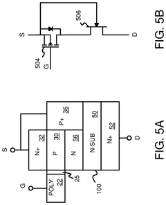
- An integrated MOSFET-JFET device with ON-resistance trimming p-islands is developed, where the geometry of P islands is optimized to shape the I-V curve, reducing ON resistance in the linear region and saturation current in the saturation region.
Thermal Management Considerations for SiC Devices
Thermal management represents a critical aspect of SiC MOSFET implementation in power electronic systems. Unlike traditional silicon devices, SiC MOSFETs operate at significantly higher temperatures and power densities, necessitating specialized thermal design considerations. The thermal conductivity of SiC (approximately 3.7 W/cm·K) exceeds that of silicon (1.5 W/cm·K), allowing for more efficient heat dissipation, yet the concentrated power density in these devices creates unique thermal challenges.
Accurate thermal modeling within circuit simulations requires comprehensive understanding of the temperature-dependent characteristics of SiC MOSFETs. The on-resistance (RDS(on)) of these devices exhibits less temperature sensitivity compared to silicon counterparts, but still increases with temperature, affecting conduction losses. Similarly, switching losses demonstrate temperature dependence that must be precisely captured in simulation models to predict device behavior across operating conditions.
Junction temperature management emerges as paramount for SiC MOSFET reliability and performance. While these devices can theoretically operate at junction temperatures up to 600°C, practical limitations from packaging materials typically restrict operation to 175-200°C. Simulation models must accurately represent the relationship between power dissipation and junction temperature rise to prevent thermal runaway conditions and ensure reliable operation.
Advanced cooling solutions specifically designed for SiC applications have become essential. Traditional air cooling often proves insufficient for high-power SiC applications, driving adoption of liquid cooling, phase-change materials, and direct substrate cooling techniques. Simulation models must incorporate these cooling system dynamics to accurately predict thermal performance under various operating conditions.
Transient thermal behavior presents particular challenges in SiC MOSFET applications. The rapid switching capabilities of these devices (often exceeding 100 kHz) create complex thermal cycling patterns that can impact long-term reliability. Accurate circuit simulation requires models that capture both steady-state and transient thermal responses, including the effects of thermal capacitance and thermal resistance across different time scales.
Package thermal resistance represents another critical parameter for SiC MOSFET modeling. The thermal path from junction to case to ambient significantly influences device performance. Advanced packaging technologies like direct bonded copper (DBC) substrates and silver sintering have emerged specifically to address SiC thermal requirements, reducing thermal resistance and improving reliability under high-temperature operation.
Reliability Testing Frameworks for SiC Models
Reliability testing frameworks for SiC MOSFET models represent a critical component in validating simulation accuracy under various operational conditions. These frameworks must address the unique characteristics of silicon carbide devices, particularly their behavior under high temperature, high voltage, and high-frequency operations where traditional silicon-based testing methodologies prove inadequate.
The development of comprehensive reliability testing frameworks typically incorporates multiple validation stages. First, static parameter verification ensures that fundamental device characteristics such as threshold voltage, on-resistance, and breakdown voltage are accurately represented across temperature ranges from -55°C to 300°C. This stage is essential as SiC MOSFETs exhibit distinctive temperature dependencies that differ significantly from silicon counterparts.
Dynamic switching behavior validation forms the second critical component, where turn-on and turn-off transients are rigorously tested against hardware measurements. Advanced frameworks implement automated test benches that can capture nanosecond-level switching events under various gate drive conditions, load configurations, and junction temperatures. These measurements are then compared with simulation results to quantify model accuracy during switching transitions.
Long-term reliability assessment constitutes another vital element in these frameworks. Accelerated stress testing protocols simulate device aging through repeated thermal cycling, gate stress, and high-voltage blocking tests. Models must accurately predict performance degradation patterns, particularly threshold voltage shifts and increased on-resistance over time, which are common reliability concerns in SiC technology.
Statistical validation approaches have emerged as essential components in modern testing frameworks. Monte Carlo simulations incorporating manufacturing process variations help quantify model robustness across device-to-device variations. This statistical dimension is particularly important for SiC MOSFETs where process maturity continues to evolve and parameter spread can be significant.
Industry-standard benchmark circuits provide the final validation layer in comprehensive frameworks. These include half-bridge configurations, buck/boost converters, and three-phase inverters operating under application-specific conditions. Performance metrics such as efficiency, switching losses, and electromagnetic interference (EMI) generation are measured and compared against simulation predictions to verify model accuracy in realistic circuit environments.
The implementation of automated regression testing systems ensures model consistency across software versions and device generations. These systems maintain historical validation data and automatically flag deviations when model updates are implemented, providing traceability and confidence in simulation results over time.
Unlock deeper insights with PatSnap Eureka Quick Research — get a full tech report to explore trends and direct your research. Try now!
Generate Your Research Report Instantly with AI Agent
Supercharge your innovation with PatSnap Eureka AI Agent Platform!