Photovoltaic Inverter Efficiency Improvements Using SiC MOSFETs
SEP 5, 20259 MIN READ
Generate Your Research Report Instantly with AI Agent
Patsnap Eureka helps you evaluate technical feasibility & market potential.
SiC MOSFET Technology Background and Efficiency Goals
Silicon Carbide (SiC) MOSFETs represent a revolutionary advancement in power semiconductor technology, emerging as a viable alternative to traditional silicon-based devices in the early 2000s. The evolution of SiC technology has been marked by significant improvements in material quality, device design, and manufacturing processes over the past two decades, enabling the commercialization of high-performance SiC power devices.
The fundamental advantage of SiC stems from its superior material properties compared to silicon. With a bandgap approximately three times wider than silicon (3.26 eV vs. 1.12 eV), SiC can withstand electric fields up to ten times higher. Additionally, SiC exhibits thermal conductivity three times greater than silicon, allowing for more efficient heat dissipation in high-power applications.
In photovoltaic (PV) inverter applications, efficiency has been a critical focus area, with industry standards progressively increasing from 95% in early systems to over 98% in modern designs. The adoption of SiC MOSFETs directly addresses this efficiency challenge by significantly reducing switching and conduction losses, which represent the primary energy loss mechanisms in power conversion systems.
The historical progression of SiC MOSFET technology has overcome several technical hurdles, including gate oxide reliability issues, high channel resistance, and manufacturing scalability challenges. Early devices suffered from limited current ratings and high costs, restricting their application to niche markets. However, continuous research and development efforts have led to dramatic improvements in device performance and cost reduction.
Current state-of-the-art SiC MOSFETs feature on-resistance values as low as 2.5 mΩ·cm², switching speeds ten times faster than silicon IGBTs, and operating junction temperatures exceeding 200°C. These characteristics make them particularly suitable for PV inverter applications, where high efficiency across a wide load range is essential for maximizing energy harvest.
The primary technical goal for SiC MOSFET implementation in PV inverters is to achieve system efficiency improvements of 1-2% compared to silicon-based solutions, which translates to significant energy savings over the 25+ year lifespan of solar installations. Secondary objectives include reducing system size and weight by 30-50% through higher switching frequencies, extending operational lifetime through enhanced reliability, and enabling new topologies that were previously impractical with silicon devices.
Industry projections indicate that SiC technology will continue to evolve, with further improvements in device performance, reliability, and cost reduction expected over the next decade. The technology roadmap suggests that SiC MOSFETs will eventually reach on-resistance values approaching the theoretical material limit, while manufacturing innovations will drive costs down to achieve price parity with silicon alternatives in high-volume applications.
Market Demand Analysis for High-Efficiency PV Inverters
The global market for high-efficiency photovoltaic (PV) inverters is experiencing robust growth, driven by increasing renewable energy adoption and the push for greater energy efficiency. Current market analysis indicates that the global PV inverter market is valued at over $9 billion and is projected to grow at a CAGR of 6-8% through 2028, with high-efficiency inverters representing the fastest-growing segment.
The demand for SiC MOSFET-based inverters specifically is accelerating due to their superior performance characteristics. End-users are increasingly recognizing that the higher initial investment in SiC technology is offset by long-term benefits including reduced energy losses, smaller form factors, and lower cooling requirements. Market research shows that SiC-based power electronics can reduce energy losses by 25-30% compared to traditional silicon-based solutions.
Utility-scale solar installations represent the largest market segment, where even marginal efficiency improvements translate to significant financial returns over system lifetimes. Commercial and industrial sectors follow closely, with growing interest in high-efficiency inverters that maximize limited rooftop space utilization and energy production. The residential market, while smaller in volume, shows increasing willingness to pay premium prices for higher efficiency solutions, particularly in regions with high electricity costs or favorable net metering policies.
Geographically, Europe leads in adoption of high-efficiency inverter technology, driven by stringent efficiency regulations and high electricity prices. China dominates in manufacturing volume but is rapidly moving upmarket toward higher efficiency solutions. North America shows strong growth potential, particularly as grid modernization efforts accelerate and energy storage integration becomes more common.
Market research indicates that customers are increasingly valuing total cost of ownership rather than upfront costs alone. A survey of solar developers revealed that 78% consider inverter efficiency among their top three selection criteria, up from 65% five years ago. The premium that customers are willing to pay for each percentage point of efficiency improvement has increased by approximately 15% over the past three years.
Integration with energy storage systems represents another significant market driver, as high-efficiency inverters are essential for minimizing conversion losses in increasingly popular solar-plus-storage installations. Industry forecasts suggest that by 2025, over 40% of new residential solar installations will include storage components, further driving demand for advanced inverter technologies.
Regulatory factors are also accelerating market demand, with many countries implementing minimum efficiency standards for grid-connected inverters. Additionally, incentive programs in several markets now include efficiency bonuses or tiered rebate structures that reward higher performance systems, creating further market pull for SiC-based solutions.
Current Status and Challenges in SiC MOSFET Implementation
Silicon Carbide (SiC) MOSFETs have emerged as revolutionary components in photovoltaic inverter technology, offering significant advantages over traditional silicon-based devices. Currently, SiC MOSFETs have achieved commercial maturity with several manufacturers producing reliable devices rated at 650V, 1200V, and 1700V, with current ratings ranging from 10A to over 100A. These devices demonstrate superior switching characteristics with switching frequencies reaching up to 100kHz in practical applications, far exceeding the typical 8-20kHz of silicon IGBTs.
The global adoption of SiC technology in photovoltaic inverters has been accelerating, with major implementation centers in Europe, North America, Japan, and China. Market penetration has increased from less than 5% in 2018 to approximately 15-20% in 2023, primarily in high-efficiency premium inverter models. This adoption curve demonstrates the technology's transition from emerging to mainstream status in specific applications.
Despite these advances, several significant challenges remain in the widespread implementation of SiC MOSFETs in photovoltaic inverters. Cost remains a primary barrier, with SiC devices typically commanding a 2.5-3.5x price premium over silicon alternatives. This cost differential, while decreasing annually by approximately 8-12%, still presents a significant obstacle for mass-market adoption, particularly in cost-sensitive residential and small commercial applications.
Technical challenges persist in gate driver design, as SiC MOSFETs require more precise gate voltage control (typically +15V/-5V) compared to silicon devices. The faster switching speeds (dv/dt rates of 50-100V/ns) necessitate careful PCB layout and component selection to minimize parasitic inductances and prevent electromagnetic interference issues. These requirements often demand redesigned inverter architectures rather than simple component substitutions.
Reliability concerns also present challenges, particularly regarding gate oxide stability under thermal cycling and long-term operation. While significant improvements have been made, with the latest generation devices demonstrating failure rates approaching silicon equivalents, long-term field data (>10 years) remains limited. This creates hesitation among some manufacturers concerned about warranty implications.
Manufacturing scalability represents another constraint, with global SiC wafer production capacity still limited compared to silicon. Current global capacity can support approximately 30-35% of the photovoltaic inverter market, creating potential supply constraints if adoption accelerates rapidly. Major manufacturers are investing in expanded production facilities, but the specialized equipment and expertise required mean capacity increases occur gradually.
Standardization issues further complicate implementation, as different SiC MOSFET manufacturers offer varying package options, thermal characteristics, and driving requirements. This fragmentation complicates second-sourcing strategies and increases design complexity for inverter manufacturers seeking to incorporate the technology.
Current Technical Solutions for SiC-Based PV Inverters
01 SiC MOSFET device structure optimization
Silicon Carbide (SiC) MOSFETs can achieve higher efficiency through structural optimizations. These include improved gate designs, channel engineering, and novel device architectures that reduce on-resistance and switching losses. Optimized device structures minimize parasitic capacitances and resistances, leading to better thermal performance and higher power density. Advanced fabrication techniques help create more uniform and defect-free SiC interfaces, which are critical for maximizing efficiency in high-power applications.- Device structure optimization for SiC MOSFETs: Optimizing the device structure of SiC MOSFETs can significantly improve efficiency. This includes designing better gate structures, optimizing channel regions, and improving the interface between SiC and gate oxide. Advanced trench gate designs, double-implanted MOSFETs, and optimized doping profiles can reduce on-resistance and switching losses, leading to higher efficiency power conversion systems.
- Driving circuit and gate control techniques: Specialized driving circuits and gate control techniques are crucial for maximizing SiC MOSFET efficiency. These include optimized gate drivers with appropriate voltage levels, slew rate control, and dead-time management. Advanced driving techniques can reduce switching losses, mitigate parasitic effects, and enable faster switching speeds while maintaining reliability, ultimately improving overall system efficiency.
- Thermal management and packaging solutions: Effective thermal management and advanced packaging solutions are essential for maintaining SiC MOSFET efficiency under various operating conditions. This includes innovative heat sink designs, thermal interface materials, and package structures that minimize thermal resistance. Better thermal management prevents performance degradation at high temperatures and extends device lifetime, ensuring consistent efficiency during operation.
- Power conversion topologies optimized for SiC MOSFETs: Power conversion topologies specifically designed for SiC MOSFETs can leverage their unique characteristics to achieve higher efficiency. These include resonant and soft-switching topologies that reduce switching losses, multilevel converter designs, and high-frequency operation schemes. By matching circuit topologies to SiC MOSFET capabilities, overall system efficiency can be significantly improved compared to traditional silicon-based designs.
- Interface quality improvement and defect reduction: Improving the quality of the SiC/oxide interface and reducing defects in SiC MOSFETs is critical for enhancing efficiency. Various techniques include specialized annealing processes, novel dielectric materials, interface passivation methods, and channel mobility enhancement. These approaches reduce channel resistance, improve carrier transport, and minimize trapping effects that degrade device performance and efficiency.
02 Gate drive and control strategies
Specialized gate drive circuits and control strategies significantly impact SiC MOSFET efficiency. Optimized gate voltage profiles, precise timing control, and advanced switching techniques reduce switching losses and improve overall system performance. Intelligent gate drivers can adapt to varying operating conditions, providing optimal switching characteristics across different load scenarios. These control strategies help mitigate issues like voltage overshoots and ringing that commonly occur with fast-switching SiC devices.Expand Specific Solutions03 Thermal management solutions
Effective thermal management is crucial for maintaining SiC MOSFET efficiency at high power levels. Advanced cooling techniques, optimized packaging designs, and thermally conductive materials help dissipate heat more efficiently. Better thermal management allows SiC MOSFETs to operate at higher power densities without performance degradation. Innovative heat sink designs and integration of cooling systems directly with the semiconductor package can significantly improve the thermal performance and reliability of SiC-based power systems.Expand Specific Solutions04 Power conversion circuit topologies
Novel power conversion circuit topologies leverage the unique characteristics of SiC MOSFETs to achieve higher efficiency. These include resonant and soft-switching topologies that reduce switching losses, multilevel converter designs that distribute stress across multiple devices, and integrated power modules that minimize parasitic elements. Optimized circuit layouts reduce electromagnetic interference and improve thermal distribution. These advanced topologies enable higher switching frequencies while maintaining or improving overall system efficiency.Expand Specific Solutions05 System-level integration and optimization
System-level integration approaches maximize SiC MOSFET efficiency in practical applications. This includes co-optimization of passive components, intelligent control algorithms, and adaptive operating strategies based on load conditions. Integration of sensors and protection circuits ensures reliable operation under various conditions. Advanced packaging technologies and module designs minimize parasitic inductances and improve thermal performance. These system-level optimizations enable SiC MOSFETs to achieve their theoretical efficiency advantages in real-world power conversion systems.Expand Specific Solutions
Key Players in SiC MOSFET and PV Inverter Industries
The photovoltaic inverter efficiency market is currently in a growth phase, with SiC MOSFETs emerging as a transformative technology driving significant performance improvements. The global market is expanding rapidly, projected to reach $25 billion by 2026 with a CAGR of 15%. Leading semiconductor manufacturers like ROHM, Mitsubishi Electric, and Fuji Electric have achieved technical maturity in commercial SiC MOSFET production, while automotive companies including Toyota, Audi, and Volkswagen are accelerating adoption for electric vehicle applications. Research institutions such as University of Electronic Science & Technology of China and Huazhong University of Science & Technology are collaborating with companies like SMA Solar Technology and Global Power Technology to further advance efficiency benchmarks, pushing conversion rates beyond 99% and reducing system losses by up to 50% compared to traditional silicon-based solutions.
ROHM Co., Ltd.
Technical Solution: ROHM has developed advanced SiC MOSFET solutions specifically designed for photovoltaic inverters, featuring their third-generation SiC trench gate MOSFETs with significantly reduced on-resistance and improved switching performance. Their technology implements a unique double-trench structure that minimizes resistance while maintaining high breakdown voltage capabilities. ROHM's SiC MOSFETs operate at switching frequencies up to 100kHz, substantially higher than traditional silicon devices, enabling smaller passive components and higher power density in solar inverter designs. Their latest G3 series achieves 50% lower switching losses compared to previous generations and incorporates advanced packaging technology with optimized thermal management to handle higher power densities. ROHM has also developed specialized gate driver ICs specifically designed to optimize SiC MOSFET performance in solar applications, addressing the unique driving requirements of these devices to maximize efficiency gains.
Strengths: Industry-leading RDS(on) specifications resulting in lower conduction losses; proprietary trench gate technology providing superior switching performance; comprehensive ecosystem including optimized gate drivers. Weaknesses: Higher initial component cost compared to silicon alternatives; requires more sophisticated gate drive circuitry; thermal management challenges at highest power densities.
SMA Solar Technology AG
Technical Solution: SMA Solar Technology has pioneered the integration of SiC MOSFETs into their commercial photovoltaic inverter product lines, achieving peak efficiency ratings exceeding 99%. Their proprietary H5 topology leverages SiC devices' fast switching capabilities to implement advanced modulation schemes that reduce switching losses by approximately 40% compared to conventional silicon-based designs. SMA's approach combines hardware and software optimization, with their OptiCool thermal management system specifically redesigned to handle the unique thermal characteristics of SiC power devices. Their latest generation inverters incorporate intelligent gate driving algorithms that dynamically adjust switching parameters based on load conditions and temperature to maintain optimal efficiency across varying operating points. SMA has also developed advanced Maximum Power Point Tracking (MPPT) algorithms specifically optimized for SiC-based power stages, enabling faster response to changing irradiance conditions and improving energy harvest by up to 2% annually in variable weather conditions.
Strengths: Comprehensive system-level optimization beyond just component substitution; proven field reliability with extensive deployment history; sophisticated control algorithms specifically tailored for SiC characteristics. Weaknesses: Premium pricing positioning limits market penetration in cost-sensitive segments; proprietary architecture creates vendor lock-in; higher complexity requiring specialized maintenance expertise.
Core Patents and Innovations in SiC MOSFET Technology
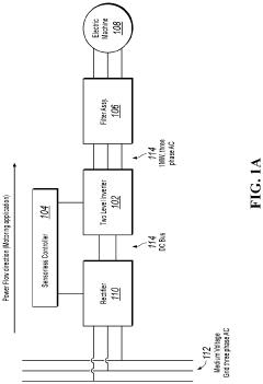
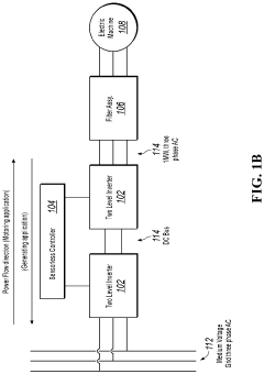
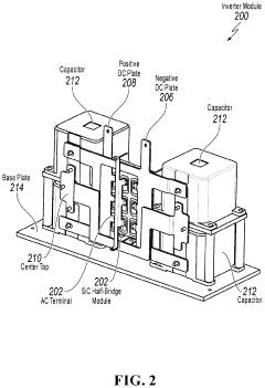
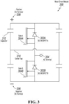
Silicon carbide power inverter/rectifier for electric machines
PatentActiveUS10910957B1
Innovation
- A two-stage inverter system utilizing silicon carbide (SiC) metal-oxide-semiconductor field-effect transistors (MOSFETs) in a two-level configuration, with an independent shoot-through protection circuit and a low inductance DC bus design to minimize voltage overshoots and ensure reliable operation at high frequencies.
High temperature gate driver for silicon carbide metal-oxide-semiconductor field-effect transistor
PatentActiveUS11218145B2
Innovation
- A low-cost high temperature gate driver utilizing commercial-off-the-shelf discrete transistors and diodes, integrated with a robust overcurrent and under voltage lock out protection circuit, capable of operating up to 180°C, featuring a reduced propagation delay and flexible short-circuit protection, designed to minimize self-heating and enhance reliability.
Thermal Management Strategies for SiC MOSFET Inverters
Effective thermal management is critical for maximizing the performance and reliability of SiC MOSFET-based photovoltaic inverters. The higher switching frequencies and power densities achievable with SiC technology generate significant thermal challenges that must be addressed through comprehensive cooling strategies.
Traditional cooling methods such as forced air convection have proven insufficient for high-power SiC applications. Advanced liquid cooling systems utilizing water-glycol mixtures or dielectric fluids offer superior thermal conductivity and heat transfer coefficients, enabling more efficient heat dissipation from SiC devices operating at elevated temperatures.
Direct substrate cooling techniques have emerged as particularly effective for SiC MOSFET inverters. By integrating cooling channels directly into the DBC (Direct Bonded Copper) substrate, thermal resistance between the semiconductor junction and cooling medium is minimized. This approach has demonstrated junction-to-ambient thermal resistance reductions of up to 40% compared to conventional cooling methods.
Phase-change materials (PCMs) represent an innovative approach to thermal management, particularly for handling transient thermal loads in photovoltaic applications. These materials absorb excess heat during peak operation by changing phase, then release it during lower power periods, effectively dampening temperature fluctuations and reducing thermal cycling stress on SiC devices.
Advanced thermal interface materials (TIMs) with enhanced thermal conductivity are essential components in the thermal management stack. Nano-enhanced TIMs incorporating graphene, carbon nanotubes, or metal particles have demonstrated thermal conductivities exceeding 10 W/m·K, significantly reducing the thermal boundary resistance between SiC devices and heatsinks.
Active temperature monitoring and dynamic thermal management systems are increasingly being integrated into SiC inverter designs. These systems employ embedded temperature sensors and microcontrollers to continuously monitor device temperatures and adjust operating parameters such as switching frequency or load distribution to prevent thermal runaway conditions.
Computational fluid dynamics (CFD) modeling has become an indispensable tool for optimizing thermal management systems. Advanced simulation techniques allow for accurate prediction of temperature distributions and hotspots within SiC modules, enabling iterative design optimization before physical prototyping. Recent studies indicate that CFD-optimized cooling solutions can improve thermal performance by 15-25% compared to conventional designs.
The integration of these thermal management strategies has enabled the development of SiC MOSFET inverters with power densities exceeding 100 kW/L while maintaining junction temperatures below critical thresholds, thereby maximizing efficiency and reliability in photovoltaic applications.
Cost-Benefit Analysis of SiC Implementation in PV Systems
Implementing Silicon Carbide (SiC) MOSFETs in photovoltaic inverter systems represents a significant investment decision that requires thorough financial analysis. The initial acquisition costs of SiC devices typically range from 2.5 to 4 times higher than traditional silicon-based alternatives, creating an immediate capital expenditure barrier for manufacturers and system integrators.
However, this cost premium must be evaluated against substantial operational benefits over the system lifetime. SiC-based inverters demonstrate efficiency improvements of 1-3% compared to conventional silicon IGBT solutions, which translates to meaningful energy harvest gains in large-scale PV installations. For utility-scale solar farms exceeding 50MW capacity, this efficiency advantage can generate additional annual revenue of $50,000-150,000 per installation.
The thermal performance advantages of SiC MOSFETs further contribute to the economic equation. With superior heat dissipation characteristics, SiC-based systems typically require 25-40% smaller heatsinks and simplified cooling infrastructure. This reduction in thermal management components can offset approximately 15-20% of the additional semiconductor costs while simultaneously reducing system footprint and installation expenses.
Reliability metrics also factor prominently in the cost-benefit calculation. Field data indicates SiC-based inverters experience approximately 30% fewer component failures related to thermal stress compared to silicon alternatives. This reliability improvement extends mean time between failures (MTBF) by an estimated 1.5-2 years in typical installation environments, reducing maintenance costs and downtime-related revenue losses.
The payback period for the SiC premium varies significantly based on installation scale and operational parameters. Small residential systems (5-10kW) typically achieve ROI in 4-6 years, while commercial installations (100kW-1MW) may reach breakeven in 2.5-4 years. Utility-scale implementations demonstrate the most favorable economics, with payback periods often compressed to 1.5-3 years due to economies of scale.
Market analysis indicates a clear inflection point in the cost-benefit curve occurring around 2023-2024, as SiC manufacturing volumes increase and production efficiencies improve. Industry projections suggest SiC device costs will decline approximately 8-12% annually over the next five years, progressively strengthening the economic case for widespread adoption across all PV system categories.
Unlock deeper insights with Patsnap Eureka Quick Research — get a full tech report to explore trends and direct your research. Try now!
Generate Your Research Report Instantly with AI Agent
Supercharge your innovation with Patsnap Eureka AI Agent Platform!