How Do SiC MOSFETs Improve Power Factor Correction Circuits?
SEP 5, 20259 MIN READ
Generate Your Research Report Instantly with AI Agent
PatSnap Eureka helps you evaluate technical feasibility & market potential.
SiC MOSFET Evolution and PFC Enhancement Goals
Silicon Carbide (SiC) MOSFETs have undergone significant evolution since their commercial introduction in the early 2000s. Initially, these devices faced challenges related to manufacturing consistency, gate oxide reliability, and high production costs. The technology has progressed through several generations, with each iteration addressing specific limitations while enhancing performance characteristics. Early SiC MOSFETs operated at lower switching frequencies with relatively high on-resistance compared to today's standards, limiting their practical applications despite their theoretical advantages over silicon.
The evolution trajectory has been marked by continuous improvements in device structure, manufacturing processes, and material quality. Second-generation devices introduced around 2010-2012 demonstrated substantial reductions in on-resistance and improved thermal performance. By the third generation (circa 2015-2017), manufacturers achieved significant breakthroughs in channel mobility and gate oxide reliability, enabling higher operating voltages and better switching performance.
Current generation SiC MOSFETs feature dramatically reduced switching losses, enhanced thermal conductivity, and significantly lower RDS(on) values. These improvements have been achieved through innovations in cell structure design, advanced epitaxial growth techniques, and refined manufacturing processes that minimize defect densities in the crystal structure. The progression has enabled devices that can operate efficiently at junction temperatures exceeding 200°C while maintaining reliability.
In the context of Power Factor Correction (PFC) circuits, the technological evolution of SiC MOSFETs has been driven by several specific enhancement goals. Primary among these is the reduction of switching and conduction losses to improve overall energy efficiency. Modern PFC circuits demand semiconductors capable of operating at higher frequencies to reduce passive component sizes while maintaining or improving efficiency metrics.
Another critical goal has been increasing power density, allowing for more compact PFC solutions without thermal management compromises. This objective aligns with the broader industry trend toward miniaturization of power electronics in applications ranging from server power supplies to electric vehicle onboard chargers.
Reliability enhancement under high-temperature operation represents another key evolutionary target. PFC circuits in industrial applications and renewable energy systems often operate in harsh environments, necessitating components with robust performance across wide temperature ranges. The evolution of SiC technology has progressively addressed this requirement through improved packaging technologies and intrinsic material advantages.
The roadmap for future SiC MOSFET development in PFC applications focuses on further reducing specific on-resistance, enhancing short-circuit capability, and improving gate driver compatibility. These goals aim to enable the next generation of PFC topologies that can achieve power factor values approaching unity while minimizing total harmonic distortion and electromagnetic interference.
Market Demand for High-Efficiency PFC Solutions
The global market for Power Factor Correction (PFC) solutions is experiencing robust growth driven by increasing energy efficiency regulations and the rising cost of electricity. According to recent market analyses, the global power electronics market, which includes PFC circuits, is projected to reach $25 billion by 2026, with high-efficiency PFC solutions representing a significant growth segment within this market.
Energy efficiency standards such as 80 PLUS for power supplies, IEC 61000-3-2 for harmonic current emissions, and Energy Star certification are becoming increasingly stringent worldwide. These regulations are compelling manufacturers to adopt advanced PFC technologies that can achieve power factors closer to unity while maintaining high efficiency across varying load conditions.
Data centers represent one of the fastest-growing markets for high-efficiency PFC solutions. With global data center electricity consumption reaching approximately 200 TWh annually and growing at 15% per year, operators are under immense pressure to reduce energy costs and carbon footprints. PFC circuits utilizing SiC MOSFETs can reduce power conversion losses by up to 40% compared to traditional silicon-based solutions, translating to millions in operational cost savings for large facilities.
The electric vehicle (EV) charging infrastructure market is another critical driver for advanced PFC technologies. As EV adoption accelerates globally, the demand for faster charging solutions with minimal grid impact is intensifying. High-efficiency PFC circuits are essential for Level 2 and Level 3 chargers to maintain grid stability while delivering maximum power to vehicles. The global EV charging infrastructure market is expected to grow at a CAGR of 33.4% through 2028, creating substantial demand for SiC-based PFC solutions.
Renewable energy systems, particularly solar inverters and wind power converters, represent another significant market segment. These applications require high-efficiency power conversion to maximize energy harvest from intermittent sources. The improved switching characteristics of SiC MOSFETs enable higher frequency operation in PFC stages, allowing for smaller passive components and higher power density—critical factors for space-constrained renewable energy installations.
Consumer electronics manufacturers are also seeking more efficient power supplies to meet energy regulations and consumer demand for faster charging and smaller adapters. The transition to USB-C Power Delivery standards up to 240W is driving adoption of high-performance PFC circuits in compact form factors, where the thermal and efficiency advantages of SiC MOSFETs become particularly valuable.
Industrial motor drives, which account for approximately 45% of global electricity consumption, represent another substantial market for high-efficiency PFC solutions. The improved harmonics control and higher efficiency offered by advanced PFC circuits directly translate to operational cost savings in manufacturing environments.
SiC MOSFET Technology Status and Challenges
Silicon Carbide (SiC) MOSFET technology has reached a significant level of maturity in recent years, with commercial products now widely available from multiple manufacturers. However, the technology still faces several challenges that limit its broader adoption in power factor correction (PFC) circuits and other power electronics applications.
The current state of SiC MOSFET technology demonstrates superior performance characteristics compared to traditional silicon-based devices, including higher breakdown voltage capabilities (typically 650V to 1700V), faster switching speeds, and better thermal conductivity. These properties enable PFC circuits to operate at higher frequencies with reduced switching losses, ultimately leading to more compact and efficient power conversion systems.
Despite these advantages, SiC MOSFETs face manufacturing challenges that impact yield rates and production costs. The crystal growth process for SiC wafers remains complex, with defect densities still higher than those in mature silicon processes. These defects can lead to reliability issues and performance variations across production batches, creating concerns for high-volume applications where consistency is critical.
Channel mobility in SiC MOSFETs continues to be lower than theoretical predictions due to interface traps at the SiC/SiO2 boundary. This results in higher on-resistance than ideal, partially offsetting the material's inherent advantages. Research efforts are focused on improving gate oxide quality and interface characteristics to address this limitation.
Packaging technology represents another significant challenge. The full benefits of SiC MOSFETs can only be realized with advanced packaging solutions that minimize parasitic inductances and can withstand the higher operating temperatures these devices enable. Traditional packaging methods often become the limiting factor in high-frequency PFC applications.
Cost remains a major barrier to widespread adoption. Current SiC MOSFETs typically cost 3-5 times more than their silicon counterparts, making them economically viable primarily in applications where efficiency improvements or size reductions justify the premium. Manufacturing economies of scale are gradually reducing this gap, but silicon devices maintain a significant cost advantage.
Geographically, SiC MOSFET technology development is concentrated in the United States, Japan, and Europe, with companies like Wolfspeed, ROHM, and Infineon leading innovation. China has made significant investments to develop domestic SiC capabilities, while South Korea is also emerging as a player in this space.
Reliability and long-term performance data for SiC MOSFETs in PFC applications is still being accumulated. While accelerated testing shows promising results, real-world operational experience over extended periods is limited compared to silicon devices with decades of field data.
Current SiC-based PFC Circuit Topologies
01 SiC MOSFET-based PFC circuit topologies
Silicon Carbide (SiC) MOSFETs can be implemented in various power factor correction (PFC) circuit topologies to improve efficiency and power density. These topologies include bridgeless PFC, totem-pole PFC, and interleaved PFC configurations. The superior switching characteristics of SiC MOSFETs allow for higher switching frequencies, reduced switching losses, and improved thermal performance in these circuits, resulting in more compact and efficient power conversion systems.- SiC MOSFET-based PFC circuit topologies: Various circuit topologies are employed for power factor correction using SiC MOSFETs. These include bridgeless PFC circuits, interleaved boost converters, and totem-pole configurations that leverage the superior switching characteristics of SiC devices. These topologies help reduce switching losses, improve power density, and achieve higher efficiency compared to traditional silicon-based designs. The implementation of these advanced circuit configurations enables operation at higher frequencies while maintaining thermal stability.
- Gate driving techniques for SiC MOSFETs in PFC applications: Specialized gate driving techniques are essential for optimizing SiC MOSFET performance in power factor correction circuits. These include adaptive gate driving, resonant gate drivers, and multi-level driving schemes that address the unique characteristics of SiC devices. Proper gate driving helps minimize switching losses, reduce electromagnetic interference, and ensure reliable operation across varying load conditions. Advanced gate control strategies also enable faster switching transitions while protecting the device from voltage spikes and oscillations.
- Thermal management and reliability of SiC MOSFET PFC converters: Effective thermal management is crucial for SiC MOSFET-based power factor correction systems. Innovative cooling solutions, optimized package designs, and thermal interface materials are employed to handle the high power density of these devices. Reliability enhancement techniques include stress reduction methods, robust interconnection technologies, and failure mode analysis specific to SiC devices. These approaches extend the operational lifetime of PFC converters while allowing them to operate at higher temperatures than silicon-based alternatives.
- Control algorithms for SiC MOSFET PFC converters: Advanced control algorithms are developed specifically for SiC MOSFET-based power factor correction systems. These include digital control schemes, predictive control methods, and adaptive algorithms that optimize switching patterns based on load conditions. The control strategies enable fast dynamic response, high power factor, low total harmonic distortion, and improved efficiency across varying input voltages and load conditions. Implementation of these algorithms often involves microcontrollers or digital signal processors with specialized firmware.
- Integration of SiC MOSFETs in high-frequency PFC applications: SiC MOSFETs enable high-frequency operation in power factor correction circuits, allowing for smaller passive components and increased power density. Integration approaches include compact module designs, embedded gate drivers, and optimized layout techniques that minimize parasitic effects. High-frequency operation (typically above 100 kHz) reduces the size of magnetic components while maintaining high efficiency. These integration techniques address challenges related to electromagnetic interference, thermal coupling, and signal integrity in densely packed power converters.
02 Gate driving techniques for SiC MOSFETs in PFC applications
Specialized gate driving techniques are essential for optimizing the performance of SiC MOSFETs in power factor correction circuits. These techniques include optimized gate voltage levels, controlled slew rates, and protection mechanisms against voltage spikes. Advanced gate drivers can mitigate the challenges associated with the fast switching speeds of SiC devices, reduce electromagnetic interference, and ensure reliable operation under various load conditions while maintaining high power factor.Expand Specific Solutions03 Thermal management solutions for SiC MOSFET PFC converters
Effective thermal management is crucial for SiC MOSFET-based power factor correction converters to ensure reliability and optimal performance. Solutions include advanced packaging technologies, improved heat sink designs, and thermal interface materials with enhanced thermal conductivity. These approaches help dissipate the heat generated during high-frequency switching operations, allowing the SiC MOSFETs to operate at higher power densities while maintaining safe operating temperatures and extending the lifetime of the PFC converter.Expand Specific Solutions04 Control algorithms for SiC MOSFET PFC converters
Specialized control algorithms are developed for SiC MOSFET-based power factor correction converters to maximize their performance advantages. These algorithms include digital control techniques, predictive control methods, and adaptive control strategies that can respond to varying load conditions. The high switching speed capability of SiC MOSFETs enables implementation of more sophisticated control schemes that can achieve near-unity power factor, low total harmonic distortion, and fast dynamic response while optimizing efficiency across a wide operating range.Expand Specific Solutions05 Integration of SiC MOSFETs in multi-level PFC converters
SiC MOSFETs can be effectively integrated into multi-level power factor correction converter architectures to achieve higher voltage handling capability and improved efficiency. These multi-level topologies distribute voltage stress across multiple devices, allowing for the use of lower voltage-rated components and reducing switching losses. The fast switching characteristics of SiC MOSFETs enable these converters to operate at higher frequencies, resulting in smaller passive components, improved power density, and enhanced dynamic performance for demanding applications.Expand Specific Solutions
Key SiC MOSFET Manufacturers and Market Landscape
SiC MOSFETs in power factor correction (PFC) circuits represent a rapidly maturing technology in the power electronics industry, currently transitioning from early adoption to mainstream implementation. The market is experiencing robust growth, projected to reach $2.19 billion by 2027 with a CAGR of 33.4%. Leading companies like STMicroelectronics, Panasonic, ON Semiconductor (Semiconductor Components Industries), and Huawei are driving innovation, while Chinese firms including Yangzhou Yangjie Electronic Technology and Global Power Technology are emerging as significant competitors. Academic institutions such as Xidian University and Fudan University are contributing valuable research to advance SiC MOSFET technology, particularly in improving efficiency, reducing switching losses, and enabling higher frequency operation in PFC applications.
Panasonic Holdings Corp.
Technical Solution: Panasonic has developed a distinctive approach to SiC MOSFET technology for PFC applications, focusing on their proprietary X-GaN™ and hybrid SiC-Si solutions. Their SiC MOSFETs feature a unique double-trench structure that simultaneously minimizes on-resistance (achieving values as low as 20mΩ for 650V devices) while optimizing gate reliability. Panasonic's devices are specifically designed to address the challenges of bridgeless PFC topologies, with symmetrical switching characteristics and minimal reverse recovery effects. Their SiC MOSFETs demonstrate particularly low output capacitance (Coss) values, enabling faster switching transitions and reduced switching losses at the high frequencies (80-150kHz) commonly used in modern PFC designs. Panasonic has implemented these devices in their own power supply products, demonstrating efficiency improvements of 0.8-1.5% compared to silicon alternatives, with particularly strong performance in light-load conditions. Their SiC MOSFETs also feature enhanced avalanche ruggedness, with single-event energy handling capabilities exceeding 1J, providing additional protection against voltage spikes common in PFC circuits during grid transients.
Strengths: Excellent light-load efficiency characteristics particularly valuable for consumer electronics applications; optimized for bridgeless PFC topologies; superior output capacitance characteristics enable higher frequency operation. Weaknesses: More limited voltage range options compared to some competitors; higher cost premium over silicon alternatives; requires careful thermal management in high-power applications.
Semiconductor Components Industries LLC
Technical Solution: Semiconductor Components Industries (ON Semiconductor) has developed a comprehensive portfolio of SiC MOSFETs specifically optimized for PFC applications across various power levels. Their technology focuses on balancing performance with cost-effectiveness, making SiC more accessible for mainstream power conversion applications. ON's SiC MOSFETs feature a planar gate structure with optimized cell density to achieve low on-resistance (typically 27-80mΩ for 650-1200V devices) while maintaining excellent switching characteristics. A key innovation in their approach is the implementation of enhanced body diodes with minimal reverse recovery charge (Qrr values as low as 50nC), which is particularly beneficial for bridgeless and totem-pole PFC topologies. ON Semiconductor has demonstrated their SiC MOSFETs in critical-conduction-mode (CrM) PFC circuits operating at frequencies up to 250kHz, achieving power densities approximately 40% higher than equivalent silicon-based designs. Their devices also feature robust gate oxide reliability with accelerated lifetime testing showing minimal threshold voltage shift even after extended high-temperature gate bias stress, addressing a common concern with SiC MOSFET technology.
Strengths: Well-balanced performance-to-cost ratio making SiC more accessible for mainstream applications; excellent body diode characteristics particularly beneficial for advanced PFC topologies; comprehensive portfolio covering multiple voltage classes and current ratings. Weaknesses: Not as optimized for ultra-high frequency operation as some specialized competitors; thermal performance requires careful consideration in high-power-density designs; gate drive requirements more demanding than silicon alternatives.
Critical SiC MOSFET Parameters for PFC Applications
Silicon carbide field-effect transistors
PatentActiveUS11894454B2
Innovation
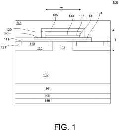
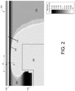
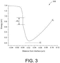
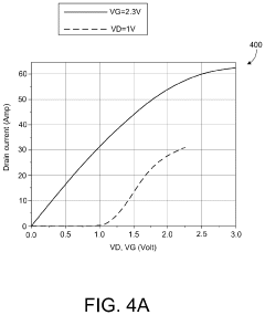
- The development of a silicon carbide (SiC) metal-oxide-semiconductor field-effect transistor (MOSFET) with a gate structure comprising a gate oxide layer, an aluminum nitride layer, and a p-type gallium nitride layer, which includes a lateral built-in channel with a p-type AlGaN gate and an AlN buffer layer, providing high threshold voltage and low interface trap density, enabling efficient operation with low on-state resistance.
Silicon carbide semiconductor device
PatentPendingUS20240234569A9
Innovation
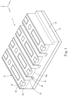
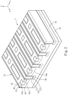
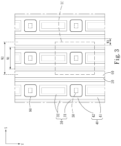
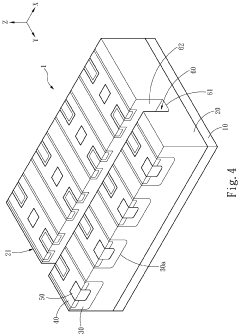
- A silicon carbide semiconductor device with a hybrid gate structure featuring a trench gate configuration that reduces JFET resistance and parasitic gate-to-drain capacitance, enhancing switching performance by increasing channel width density and optimizing the layout of doped regions and trenches.
Thermal Management Strategies for SiC PFC Circuits
Thermal management represents a critical challenge in SiC-based Power Factor Correction (PFC) circuits due to the high switching frequencies and power densities these systems typically operate at. While Silicon Carbide MOSFETs offer superior thermal conductivity compared to traditional silicon devices, effective thermal management strategies remain essential to ensure optimal performance and reliability.
The primary thermal management approach involves strategic component placement on PCB layouts. By positioning SiC MOSFETs and other heat-generating components with sufficient spacing and proximity to cooling elements, designers can facilitate more efficient heat dissipation. Advanced thermal simulation tools enable precise prediction of hotspots and optimization of component arrangements before physical prototyping.
Heat sink selection and design constitute another crucial aspect of thermal management. SiC PFC circuits benefit from specialized heat sinks with optimized fin structures and materials that match the thermal characteristics of SiC devices. Copper and aluminum alloys with enhanced thermal conductivity properties are commonly employed, with recent innovations focusing on composite materials that offer improved performance-to-weight ratios.
Active cooling solutions have evolved significantly for SiC applications. Forced-air cooling systems with intelligent fan speed control can adjust cooling capacity based on real-time temperature monitoring. For high-power applications, liquid cooling systems offer superior heat extraction capabilities, though at the cost of increased complexity and maintenance requirements.
Thermal interface materials (TIMs) play a vital role in maximizing heat transfer between SiC devices and cooling structures. Advanced ceramic-filled polymers, phase-change materials, and metal-based TIMs have been developed specifically for the temperature profiles and thermal cycling characteristics of SiC power electronics, reducing thermal resistance at critical junctions.
Innovative packaging technologies are emerging as effective thermal management solutions. Direct bonded copper (DBC) substrates and advanced module designs incorporate thermal vias and embedded cooling channels to enhance heat extraction directly from the semiconductor junction. These approaches minimize thermal resistance in the heat dissipation path, allowing SiC MOSFETs to operate closer to their theoretical performance limits.
Temperature monitoring and adaptive control systems represent the intelligence layer of thermal management. By implementing distributed temperature sensors and closed-loop control algorithms, modern SiC PFC circuits can dynamically adjust operating parameters to maintain optimal thermal conditions, extending device lifetime while maximizing performance under varying load conditions.
Cost-Performance Analysis of SiC vs Silicon Solutions
When evaluating SiC MOSFETs against traditional silicon solutions for power factor correction circuits, cost-performance analysis reveals significant trade-offs that influence implementation decisions. The initial acquisition cost of SiC MOSFETs typically ranges from 3 to 5 times higher than comparable silicon MOSFETs, presenting a substantial barrier to entry for cost-sensitive applications. This premium pricing stems from more complex manufacturing processes, lower production volumes, and relatively newer fabrication technologies.
However, the performance advantages of SiC devices often justify this higher initial investment through system-level savings. SiC MOSFETs operate efficiently at junction temperatures up to 200°C compared to silicon's typical 150°C limit, reducing cooling requirements and associated thermal management costs. The smaller die size for equivalent ratings also contributes to more compact designs, potentially reducing PCB real estate and enclosure dimensions by 30-40%.
Energy efficiency improvements represent perhaps the most compelling economic argument for SiC adoption in PFC circuits. With switching losses reduced by approximately 80% and conduction losses lowered by 50% compared to silicon counterparts, SiC-based PFC circuits typically achieve 98-99% efficiency versus 94-96% for silicon solutions. This efficiency differential translates to substantial operational cost savings over the device lifetime, particularly in high-power or continuous-operation applications.
Total cost of ownership calculations frequently favor SiC solutions when considering the complete system lifecycle. For a typical 3kW PFC application operating continuously, the energy savings from SiC implementation can offset the initial cost premium within 1-2 years of operation. Additionally, the higher reliability and longer service life of SiC devices—often exceeding 15 years compared to 10 years for silicon—further enhance their long-term economic value proposition.
Market analysis indicates a steady decline in SiC component pricing, with costs decreasing approximately 10-15% annually as manufacturing processes mature and production volumes increase. This trend is gradually narrowing the cost gap between silicon and SiC solutions, accelerating the economic viability of SiC adoption across broader application segments.
For power factor correction specifically, the cost-benefit equation strongly favors SiC in applications above 1kW where efficiency, power density, and reliability are prioritized over initial implementation cost. Below this threshold, silicon solutions often remain more economically viable unless specific performance requirements dictate otherwise.
Unlock deeper insights with PatSnap Eureka Quick Research — get a full tech report to explore trends and direct your research. Try now!
Generate Your Research Report Instantly with AI Agent
Supercharge your innovation with PatSnap Eureka AI Agent Platform!
