

Gate Oxide Reliability Challenges In SiC MOSFETs
SEP 5, 20259 MIN READ
Generate Your Research Report Instantly with AI Agent
PatSnap Eureka helps you evaluate technical feasibility & market potential.
SiC MOSFET Gate Oxide Evolution and Objectives
Silicon Carbide (SiC) MOSFETs have emerged as revolutionary power semiconductor devices, offering superior performance characteristics compared to traditional silicon-based counterparts. The evolution of SiC MOSFET technology spans several decades, beginning with early research in the 1980s that identified SiC as a promising wide bandgap semiconductor material. Initial development faced significant challenges related to crystal growth, defect density, and most critically, gate oxide reliability.
The technological trajectory accelerated in the early 2000s when researchers achieved breakthrough improvements in SiC substrate quality and epitaxial growth techniques. This period marked the transition from laboratory curiosity to commercial viability, with the first generation of SiC MOSFETs entering specialized markets. However, gate oxide reliability remained a persistent challenge, limiting widespread adoption despite the material's inherent advantages.
A pivotal advancement occurred around 2010-2015 when manufacturers developed novel oxidation processes specifically tailored for SiC, addressing the fundamental interface quality issues that had plagued earlier devices. These innovations included modified thermal oxidation techniques, post-oxidation annealing in nitric oxide environments, and interface passivation methods that significantly reduced interface trap densities.
The current technological landscape shows SiC MOSFETs gaining substantial market traction in applications demanding high efficiency, temperature tolerance, and switching performance. However, as operating voltages increase beyond 1200V toward 1700V and even 3300V ratings, gate oxide reliability challenges have reemerged as critical limiting factors for long-term device stability and performance.
The primary objective in SiC MOSFET gate oxide development is achieving a fundamental understanding of the unique degradation mechanisms at the SiC/SiO2 interface. Unlike silicon, where gate oxide technology has matured over decades, SiC presents distinct challenges due to its wider bandgap, different crystal structure, and complex oxidation chemistry. Researchers aim to develop predictive models that accurately capture threshold voltage instability, channel mobility degradation, and oxide breakdown phenomena specific to SiC devices.
Another key objective is establishing standardized reliability testing protocols tailored specifically for SiC MOSFETs. Current qualification methods largely derive from silicon-based technologies and may not adequately address SiC-specific failure modes or accurately predict device lifetime under typical application conditions.
Looking forward, the technology roadmap focuses on enabling higher voltage ratings while maintaining or improving reliability metrics. This requires innovations in both materials science and device architecture, potentially incorporating novel dielectric materials, interface engineering techniques, and advanced characterization methodologies to push beyond current performance limitations.
Market Analysis for SiC Power Devices
The Silicon Carbide (SiC) power device market has experienced remarkable growth in recent years, driven by the increasing demand for high-efficiency power electronics across multiple industries. The global SiC power device market was valued at approximately $1.1 billion in 2022 and is projected to reach $6.3 billion by 2028, representing a compound annual growth rate (CAGR) of over 33% during the forecast period.
Electric vehicles (EVs) constitute the largest application segment for SiC power devices, accounting for nearly 60% of the total market share. The automotive sector's transition toward electrification has created substantial demand for SiC MOSFETs due to their superior performance in high-temperature, high-frequency, and high-voltage applications compared to traditional silicon-based devices. Major automotive manufacturers have increasingly adopted SiC technology in their EV inverters to improve efficiency and extend driving range.
Industrial applications represent the second-largest market segment, with approximately 25% market share. SiC power devices are being integrated into motor drives, uninterruptible power supplies (UPS), and industrial automation systems. The ability of SiC MOSFETs to operate at higher switching frequencies while maintaining efficiency has made them particularly valuable in these applications, enabling smaller system footprints and reduced cooling requirements.
Renewable energy systems, particularly solar inverters and wind power converters, constitute about 10% of the SiC power device market. The push for higher energy conversion efficiency in renewable energy systems has accelerated SiC adoption, as these devices can reduce energy losses by up to 50% compared to silicon alternatives.
Regionally, Asia-Pacific dominates the SiC power device market with approximately 45% share, led by China, Japan, and South Korea. This dominance stems from the region's robust electronics manufacturing infrastructure and aggressive EV adoption policies. North America follows with 30% market share, driven by industrial applications and defense sector demand. Europe accounts for 20% of the market, primarily fueled by automotive and renewable energy applications.
The SiC power device supply chain faces challenges related to substrate availability and manufacturing complexity. Current SiC wafer production capacity struggles to meet growing demand, creating potential bottlenecks. Additionally, the gate oxide reliability issues in SiC MOSFETs represent a significant technical challenge that impacts market growth, as manufacturers must balance performance improvements with reliability concerns.
Gate Oxide Reliability Challenges and Limitations
The reliability of gate oxide in SiC MOSFETs represents one of the most significant challenges in wide bandgap semiconductor technology. Unlike silicon-based devices, SiC MOSFETs exhibit unique interface characteristics that fundamentally impact oxide reliability. The primary concern stems from the higher electric field strength in the oxide layer during device operation, which can be 2-3 times greater than in comparable silicon devices due to SiC's wider bandgap properties.
A critical limitation is the presence of carbon-related defects at the SiC/SiO2 interface. During thermal oxidation, carbon atoms from the SiC substrate can form various complexes within the oxide layer, creating trapping centers that compromise the oxide integrity. These defects manifest as higher interface trap densities (Dit), typically in the range of 10^12 to 10^13 cm^-2eV^-1, significantly higher than the 10^10 cm^-2eV^-1 observed in silicon devices.
Time-dependent dielectric breakdown (TDDB) presents another substantial reliability concern. Research indicates that SiC MOSFETs generally exhibit shorter oxide lifetimes compared to silicon counterparts when operated at similar electric fields. The acceleration factor for oxide breakdown in SiC devices shows distinctive behavior, with some studies reporting non-linear relationships between applied field and time-to-failure.
Bias temperature instability (BTI) effects are particularly pronounced in SiC MOSFETs. Both positive and negative BTI cause significant threshold voltage shifts during device operation, with magnitudes often exceeding 1V under stress conditions. The recovery characteristics also differ from silicon devices, showing slower recovery rates and larger permanent components of threshold voltage shift.
Hot carrier injection (HCI) degradation mechanisms in SiC MOSFETs demonstrate unique characteristics due to the wider bandgap. The higher energy carriers can cause more severe damage to the oxide layer, leading to accelerated degradation compared to silicon devices. This effect becomes particularly problematic in high-frequency switching applications where carriers repeatedly gain sufficient energy to damage the oxide.
The oxide reliability is further compromised by basal plane dislocations (BPDs) that propagate from the SiC substrate to the channel region. These crystallographic defects can intersect with the gate oxide, creating preferential paths for leakage current and potential breakdown sites. Studies have shown correlation between BPD density and premature oxide failure in SiC MOSFETs.
Temperature-dependent oxide reliability presents additional challenges. While SiC devices are designed for high-temperature operation, the oxide degradation mechanisms accelerate exponentially with temperature. This creates a fundamental limitation in exploiting the full temperature capability of SiC semiconductor material, as the oxide reliability often becomes the limiting factor before reaching the theoretical temperature limits of the semiconductor itself.
Current Gate Oxide Reliability Enhancement Techniques
01 Gate oxide material selection and deposition techniques
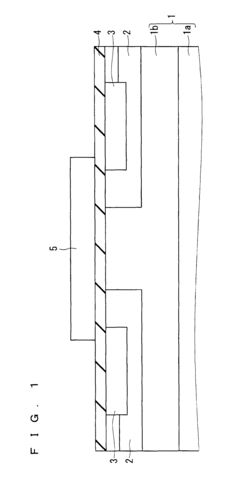
The reliability of SiC MOSFETs heavily depends on the gate oxide material selection and deposition methods. High-quality gate oxides can be formed through thermal oxidation, chemical vapor deposition (CVD), or atomic layer deposition (ALD). These techniques help in creating uniform and defect-free oxide layers that enhance the reliability of SiC MOSFETs by reducing interface traps and improving channel mobility. The selection of appropriate oxide materials, such as SiO2, Al2O3, or their combinations, plays a crucial role in determining the long-term stability and performance of the device.- Gate oxide material selection and deposition techniques: The reliability of SiC MOSFETs heavily depends on the gate oxide material selection and deposition methods. High-quality silicon dioxide (SiO2) layers can be formed through thermal oxidation, chemical vapor deposition (CVD), or atomic layer deposition (ALD). Alternative materials such as aluminum oxide (Al2O3) and hafnium oxide (HfO2) are also being explored to improve reliability. The deposition technique affects interface quality, defect density, and overall oxide reliability in high-temperature and high-electric field environments.
- Interface engineering and defect reduction: The SiC/oxide interface quality is critical for MOSFET reliability. Various interface engineering techniques are employed to reduce defect density and improve channel mobility. These include post-oxidation annealing in nitrogen or hydrogen atmospheres, nitridation processes, and interface passivation methods. Reducing carbon-related defects and dangling bonds at the interface helps minimize threshold voltage instability and channel resistance, thereby enhancing overall device reliability and performance.
- Bias temperature stress testing and reliability assessment: Evaluating gate oxide reliability in SiC MOSFETs requires specialized testing methodologies. Bias temperature stress (BTS) testing, time-dependent dielectric breakdown (TDDB) measurements, and charge trapping analysis are commonly used techniques. These tests help quantify oxide lifetime, breakdown voltage, and long-term stability under various operating conditions. Advanced characterization methods enable the identification of failure mechanisms and provide data for reliability modeling and lifetime prediction.
- Novel device structures for enhanced reliability: Innovative MOSFET structures are being developed to improve gate oxide reliability. These include trench gate designs, double-diffused structures, and shielded gate configurations that optimize electric field distribution across the oxide. Some designs incorporate buffer layers between SiC and gate oxide or utilize specialized field plates to reduce peak electric fields. These structural modifications help mitigate oxide stress and enhance reliability without compromising other device performance parameters.
- High-temperature operation and reliability enhancement: SiC MOSFETs are designed for high-temperature operation, which presents unique challenges for gate oxide reliability. Specialized oxide formulations and multi-layer dielectric stacks are being developed to withstand elevated temperatures. Techniques such as oxide densification, edge termination optimization, and specialized doping profiles help maintain oxide integrity under thermal stress. These approaches enable reliable operation in harsh environments while maintaining stable threshold voltage and minimizing leakage current over the device lifetime.
02 Interface trap density reduction methods
Interface traps at the SiC/oxide interface significantly impact the reliability of SiC MOSFETs. Various methods have been developed to reduce interface trap density, including post-oxidation annealing in nitrogen or hydrogen environments, nitridation processes, and the use of interfacial layers. These techniques help to passivate dangling bonds at the interface, leading to improved channel mobility, reduced threshold voltage instability, and enhanced overall reliability of the gate oxide in SiC MOSFETs.Expand Specific Solutions03 Novel gate stack structures for enhanced reliability
Advanced gate stack structures have been developed to enhance the reliability of SiC MOSFETs. These include multi-layer gate dielectrics, graded oxide structures, and the incorporation of high-k materials. Such novel structures help to distribute the electric field more evenly across the gate oxide, reduce leakage current, and improve resistance to high-temperature operation. The implementation of these advanced gate stack designs contributes significantly to extending the lifetime and improving the performance of SiC power devices under harsh operating conditions.Expand Specific Solutions04 Reliability testing and characterization methods
Comprehensive testing and characterization methods are essential for evaluating the reliability of SiC MOSFET gate oxides. These include time-dependent dielectric breakdown (TDDB) tests, bias temperature instability (BTI) measurements, and charge trapping analysis. Advanced characterization techniques such as deep-level transient spectroscopy (DLTS) and capacitance-voltage measurements help in understanding the degradation mechanisms and failure modes of gate oxides in SiC MOSFETs, enabling the development of more reliable devices with predictable lifetimes.Expand Specific Solutions05 Bias and temperature stress mitigation strategies
SiC MOSFET gate oxides are susceptible to degradation under bias and temperature stress conditions. Various strategies have been developed to mitigate these effects, including optimized device structures, improved edge termination designs, and specialized field plate configurations. Additionally, the incorporation of stress-relieving buffer layers and the implementation of appropriate operating guidelines help to extend the lifetime of the gate oxide under high-voltage and high-temperature conditions, which are common in power electronics applications using SiC MOSFETs.Expand Specific Solutions
Leading Manufacturers and Research Institutions
The SiC MOSFET gate oxide reliability market is currently in a growth phase, with increasing adoption across power electronics applications despite technical challenges. The market is projected to expand significantly as SiC technology matures, driven by demand for high-efficiency power devices in electric vehicles and renewable energy systems. Leading players include established semiconductor manufacturers like Infineon Technologies, ROHM, and Mitsubishi Electric, who have developed proprietary solutions for gate oxide reliability issues. Emerging competitors from China such as BASiC Semiconductor, Yangzhou Yangjie, and CRRC Times Semiconductor are rapidly advancing their capabilities. Research collaborations between industry leaders and institutions like Xidian University are accelerating technological breakthroughs in addressing interface trap density, threshold voltage instability, and oxide breakdown concerns.
ROHM Co., Ltd.
Technical Solution: ROHM has pioneered a multi-layered approach to gate oxide reliability in SiC MOSFETs through their SCT technology platform. Their solution features a proprietary double-layer gate oxide structure with different oxidation conditions for each layer to optimize interface quality. ROHM employs high-temperature hydrogen annealing processes to passivate dangling bonds at the SiC/SiO2 interface, significantly reducing interface trap density. Their technology incorporates carbon-cluster removal techniques during pre-oxidation surface preparation to minimize carbon-related defects that typically compromise oxide integrity. ROHM has also developed specialized boron diffusion processes at the gate region to reduce electric field concentration and improve threshold voltage stability. Their manufacturing process includes advanced in-situ monitoring systems that ensure precise control of oxidation parameters across production wafers.
Strengths: Excellent threshold voltage stability with drift less than 0.5V under accelerated stress testing; superior channel mobility through interface optimization techniques. Weaknesses: Complex manufacturing process with multiple critical steps increases production costs; requires specialized equipment for quality control monitoring.
General Electric Company
Technical Solution: GE has developed an advanced approach to SiC MOSFET gate oxide reliability through their silicon carbide power technology platform. Their solution features a proprietary "graded oxide" structure that creates a controlled transition region between SiC and SiO2, reducing interface stress and trap density. GE employs specialized high-temperature annealing techniques in argon-hydrogen mixtures to passivate dangling bonds and reduce oxide charges. Their technology incorporates advanced epitaxial growth processes that minimize basal plane dislocations which can propagate to the oxide interface and create reliability issues. GE has also implemented specialized screening methodologies including time-dependent dielectric breakdown (TDDB) testing under accelerated conditions to ensure long-term reliability. Their manufacturing process includes proprietary surface preparation techniques that remove subsurface damage from wafer polishing before oxidation begins.
Strengths: Excellent long-term reliability with projected lifetime exceeding 20 years at rated conditions; superior performance in high-humidity environments due to enhanced passivation techniques. Weaknesses: Limited commercial availability compared to other major players; higher initial threshold voltage variation requiring tighter sorting parameters.
Critical Patents and Research on SiC Interface Quality
Sic mosfet with transverse p+ region
PatentActiveUS20230053874A1
Innovation
- The design incorporates a silicon carbide MOSFET structure with specific doping layers and geometries, including a polysilicon gate layer, to enhance the protection of the gate oxide without increasing the MOSFET cell area, utilizing epitaxy and ion implantation processes to create N+ and P+ regions that act as shields, ensuring adequate body diode performance and channel mobility.
Method of manufacturing a semiconductor device
PatentInactiveUS8236707B2
Innovation
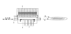
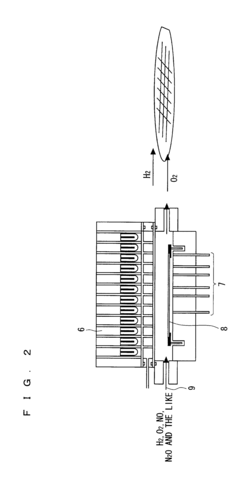
- A method involving immediate-above burning oxidation, where hydrogen and oxygen are introduced and subjected to a combustion reaction on the SiC substrate to form a silicon oxide film, utilizing O radicals for oxidation, which reduces hydroxy groups and enhances reliability, combined with subsequent dry oxidation to achieve the required thickness.
Reliability Testing Standards and Methodologies
Reliability testing standards for SiC MOSFETs have evolved significantly to address the unique challenges posed by wide bandgap semiconductor materials. The Joint Electron Device Engineering Council (JEDEC) has established several standards specifically applicable to SiC MOSFET reliability assessment, including JESD22-A108 for temperature cycling, JESD22-A110 for HTRB (High Temperature Reverse Bias), and JESD22-A118 for power cycling tests. These standards provide structured methodologies to evaluate device performance under various stress conditions.
The automotive industry, a major adopter of SiC technology, follows the AEC-Q101 qualification standard which has been adapted to address SiC-specific reliability concerns. This standard includes rigorous gate oxide integrity tests that are particularly relevant given the interface quality challenges in SiC devices. The test conditions typically involve higher voltages and temperatures compared to traditional silicon devices to account for SiC's wider operating envelope.
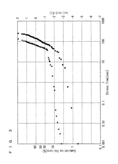
Time-Dependent Dielectric Breakdown (TDDB) testing has emerged as a critical methodology for SiC MOSFETs due to their susceptibility to gate oxide degradation. Standard TDDB tests involve applying constant voltage stress to the gate oxide while monitoring leakage current until failure occurs. For SiC devices, these tests are typically conducted at elevated temperatures (150-200°C) to accelerate the aging process and provide meaningful lifetime projections.
Bias Temperature Instability (BTI) testing has been adapted specifically for SiC MOSFETs to address their pronounced threshold voltage shifts. The standard methodology involves applying positive or negative gate bias at elevated temperatures, with periodic interruptions to measure threshold voltage changes. The recovery phenomenon in SiC devices necessitates ultra-fast measurement techniques, often requiring specialized equipment capable of sub-microsecond measurements.
Short-circuit robustness testing, while not fully standardized, follows industry-accepted methodologies that typically involve subjecting the device to short-circuit conditions for increasing durations until failure. For SiC MOSFETs, these tests are particularly important due to their smaller die size and higher power density compared to silicon counterparts.
Statistical analysis methods have also been standardized for reliability data interpretation, with Weibull distribution analysis being the predominant approach for failure time data. The acceleration factors used in reliability projections have been recalibrated for SiC technology, with activation energies typically ranging from 0.7 to 1.3 eV depending on the specific failure mechanism under investigation.
The automotive industry, a major adopter of SiC technology, follows the AEC-Q101 qualification standard which has been adapted to address SiC-specific reliability concerns. This standard includes rigorous gate oxide integrity tests that are particularly relevant given the interface quality challenges in SiC devices. The test conditions typically involve higher voltages and temperatures compared to traditional silicon devices to account for SiC's wider operating envelope.
Time-Dependent Dielectric Breakdown (TDDB) testing has emerged as a critical methodology for SiC MOSFETs due to their susceptibility to gate oxide degradation. Standard TDDB tests involve applying constant voltage stress to the gate oxide while monitoring leakage current until failure occurs. For SiC devices, these tests are typically conducted at elevated temperatures (150-200°C) to accelerate the aging process and provide meaningful lifetime projections.
Bias Temperature Instability (BTI) testing has been adapted specifically for SiC MOSFETs to address their pronounced threshold voltage shifts. The standard methodology involves applying positive or negative gate bias at elevated temperatures, with periodic interruptions to measure threshold voltage changes. The recovery phenomenon in SiC devices necessitates ultra-fast measurement techniques, often requiring specialized equipment capable of sub-microsecond measurements.
Short-circuit robustness testing, while not fully standardized, follows industry-accepted methodologies that typically involve subjecting the device to short-circuit conditions for increasing durations until failure. For SiC MOSFETs, these tests are particularly important due to their smaller die size and higher power density compared to silicon counterparts.
Statistical analysis methods have also been standardized for reliability data interpretation, with Weibull distribution analysis being the predominant approach for failure time data. The acceleration factors used in reliability projections have been recalibrated for SiC technology, with activation energies typically ranging from 0.7 to 1.3 eV depending on the specific failure mechanism under investigation.
Thermal Management Strategies for Gate Oxide Stability
Thermal management is a critical factor in ensuring gate oxide stability in SiC MOSFETs. The higher operating temperatures of SiC devices (up to 200-300°C) compared to traditional silicon counterparts create unique challenges for maintaining oxide integrity. Effective thermal management strategies must address both the intrinsic properties of SiC interfaces and the operational stresses that occur during high-temperature switching events.
Self-heating effects during device operation represent a significant concern for gate oxide reliability. When SiC MOSFETs operate at high switching frequencies or under high current densities, localized heating at the gate oxide interface can accelerate defect formation and charge trapping mechanisms. Implementation of advanced heat spreading techniques, including optimized device layouts and improved packaging solutions with enhanced thermal conductivity materials, has shown promising results in mitigating these effects.
Active cooling solutions specifically designed for SiC power modules have emerged as essential components in comprehensive thermal management strategies. These include direct liquid cooling systems that can maintain more uniform temperature distributions across the device, reducing thermal gradients that contribute to oxide stress. Some cutting-edge approaches incorporate phase-change materials within packaging to absorb thermal transients during switching events.
Temperature-aware gate driving techniques represent another frontier in thermal management for gate oxide stability. Adaptive gate driving schemes that modify switching parameters based on real-time temperature monitoring can reduce thermal stress during operation. These intelligent driving circuits can adjust slew rates and gate voltages to optimize the trade-off between switching losses and thermal stress on the gate oxide.
Thermal simulation and modeling have become indispensable tools in developing effective management strategies. Multi-physics simulation platforms that simultaneously model electrical, thermal, and mechanical stresses provide valuable insights into the complex interactions affecting gate oxide reliability. These models enable designers to identify potential hotspots and optimize thermal pathways before physical prototyping.
Recent advancements in thermally conductive die-attach materials and interface layers have shown significant improvements in heat dissipation from SiC dies. Silver-sintered die-attach materials, for example, offer superior thermal conductivity compared to traditional solders, while maintaining excellent reliability under thermal cycling conditions. These materials help maintain lower operating temperatures at the critical gate oxide interface.
Ultimately, a holistic approach to thermal management that addresses device design, packaging, cooling systems, and operational parameters is essential for ensuring long-term gate oxide stability in SiC MOSFETs. As operating temperatures and power densities continue to increase, these thermal management strategies will play an increasingly vital role in the commercial viability of SiC power devices.
Unlock deeper insights with PatSnap Eureka Quick Research — get a full tech report to explore trends and direct your research. Try now!
Generate Your Research Report Instantly with AI Agent
Supercharge your innovation with PatSnap Eureka AI Agent Platform!