Thermal Management Requirements For SiC MOSFET Devices
SEP 5, 20259 MIN READ
Generate Your Research Report Instantly with AI Agent
Patsnap Eureka helps you evaluate technical feasibility & market potential.
SiC MOSFET Thermal Evolution and Objectives
Silicon Carbide (SiC) MOSFET technology has evolved significantly since its initial development in the early 1990s. The thermal management requirements for these devices have undergone substantial transformation as the technology matured from laboratory curiosity to commercial viability. Early SiC MOSFETs suffered from poor channel mobility and high interface trap density, which limited their thermal performance and reliability at elevated temperatures.
The evolution of SiC thermal management can be traced through three distinct phases. The first phase (1990-2005) focused on fundamental material improvements, addressing defect densities and developing basic thermal dissipation techniques. During this period, researchers primarily concentrated on improving the crystal quality and reducing micropipe defects that severely impacted thermal conductivity.
The second phase (2006-2015) marked the transition to commercial viability, with significant advancements in packaging technologies specifically designed for SiC's unique thermal properties. This period saw the introduction of specialized die-attach materials capable of withstanding the higher operating temperatures of SiC devices, typically in the range of 175-200°C, compared to silicon's 125-150°C limit.
The current phase (2016-present) is characterized by system-level thermal optimization and the development of advanced cooling solutions tailored to SiC's capabilities. The focus has shifted toward enabling SiC MOSFETs to operate reliably at junction temperatures exceeding 200°C while maintaining performance advantages over silicon alternatives.
The primary objective of thermal management for SiC MOSFETs is to maximize the utilization of their inherent temperature advantages while ensuring long-term reliability. This includes developing packaging solutions that can withstand the thermal cycling stresses associated with high-temperature operation and designing cooling systems that efficiently extract heat from these high-power-density devices.
Another critical objective is to establish accurate thermal modeling techniques specific to SiC devices. Traditional thermal models developed for silicon devices often prove inadequate due to SiC's different thermal conductivity profile and temperature dependencies. Advanced multi-physics simulation approaches are being developed to better predict thermal behavior under various operating conditions.
Looking forward, the thermal management roadmap for SiC MOSFETs aims to push operating temperatures beyond 250°C for specialized applications while improving cost-effectiveness of cooling solutions for mainstream adoption. This will require innovations in die-attach materials, encapsulants, and substrate technologies that can maintain mechanical integrity and electrical performance at these extreme temperatures.
Market Demand Analysis for SiC Power Electronics
The Silicon Carbide (SiC) power electronics market is experiencing unprecedented growth driven by increasing demand for high-efficiency power conversion systems across multiple industries. Current market valuations place the global SiC power device market at approximately 2 billion USD in 2023, with projections indicating a compound annual growth rate (CAGR) of 27% through 2030, potentially reaching 10 billion USD by the end of the decade.
This remarkable growth trajectory is primarily fueled by the automotive sector, particularly electric vehicles (EVs), which currently accounts for over 60% of SiC device consumption. The transition to SiC-based power electronics in EVs enables faster charging capabilities, extended range, and reduced cooling system requirements - all critical factors in consumer adoption of electric mobility solutions.
Beyond automotive applications, industrial power supplies represent the second-largest market segment, constituting roughly 15% of current demand. This sector values SiC MOSFETs for their ability to operate efficiently at higher switching frequencies, thereby reducing the size and weight of power conversion systems while improving overall energy efficiency by 20-30% compared to silicon-based alternatives.
Renewable energy systems, particularly solar inverters and wind power converters, comprise approximately 12% of the market. The superior thermal performance of SiC devices allows these systems to operate reliably in harsh environmental conditions while maintaining high efficiency, directly addressing the growing global emphasis on sustainable energy solutions.
Rail transportation and aerospace applications, though smaller in volume (approximately 8% combined), represent high-value markets with stringent reliability requirements and willingness to pay premium prices for SiC solutions that can withstand extreme operating conditions.
Regional analysis reveals that Asia-Pacific currently dominates SiC device consumption at 45% of global market share, followed by North America (30%) and Europe (20%). China specifically has emerged as both a major consumer and producer, with substantial government investments in domestic SiC manufacturing capabilities.
Market research indicates that thermal management solutions specifically designed for SiC MOSFETs represent a rapidly growing sub-segment, with specialized cooling systems, thermal interface materials, and advanced packaging solutions experiencing 35% annual growth. This acceleration stems from recognition that conventional thermal management approaches developed for silicon devices are insufficient for maximizing SiC performance benefits.
Customer surveys reveal that 78% of design engineers cite thermal management as their primary challenge when implementing SiC technology, highlighting the critical market need for integrated thermal solutions that can handle the unique characteristics of these devices.
Current Thermal Management Challenges in SiC MOSFETs
Silicon Carbide (SiC) MOSFETs represent a significant advancement in power semiconductor technology, offering superior performance compared to traditional silicon-based devices. However, these devices face substantial thermal management challenges that must be addressed to fully realize their potential in high-power applications.
The primary thermal challenge stems from SiC MOSFETs' ability to operate at significantly higher power densities and switching frequencies than silicon counterparts. While this capability enables more compact and efficient power systems, it also results in concentrated heat generation within a smaller device footprint. Current thermal management solutions designed for silicon devices often prove inadequate for handling the thermal flux densities encountered in SiC applications.
Junction temperature management presents another critical challenge. SiC MOSFETs can theoretically operate at junction temperatures exceeding 200°C, compared to silicon's typical 150°C limit. However, packaging materials, interconnects, and surrounding components frequently become the limiting factors, creating a thermal bottleneck that prevents utilizing the full temperature capability of the SiC die itself.
The thermal interface materials (TIMs) currently available exhibit insufficient thermal conductivity for optimal SiC MOSFET performance. The thermal resistance at interfaces between the die, substrate, baseplate, and heatsink creates significant barriers to heat dissipation. This interface resistance can account for over 30% of the total thermal resistance in some package designs, severely limiting overall system performance.
Transient thermal management poses unique challenges for SiC devices. Their ability to switch at higher frequencies and handle rapid load changes creates dynamic thermal profiles with steep temperature gradients and rapid thermal cycling. These conditions accelerate thermo-mechanical stress and potential failure mechanisms in both the device and its packaging materials.
Current cooling technologies face limitations when applied to SiC MOSFETs. Conventional air cooling becomes increasingly inadequate as power densities rise, while liquid cooling systems add complexity, cost, and reliability concerns. Advanced cooling solutions like two-phase cooling, jet impingement, or microfluidic cooling show promise but remain in early adoption phases for commercial SiC applications.
The thermal design process itself presents challenges due to limited modeling tools specifically calibrated for SiC devices. Accurate thermal simulation requires precise characterization of material properties, interface behaviors, and device-specific heat generation patterns across various operating conditions. Current modeling approaches often fail to capture the complex thermal dynamics of SiC MOSFETs operating at their performance limits.
Reliability testing methodologies developed for silicon devices require significant adaptation for SiC MOSFETs. The combination of higher operating temperatures, faster switching speeds, and different failure mechanisms necessitates new approaches to accelerated life testing and thermal cycling protocols to accurately predict long-term reliability in field applications.
Current Thermal Dissipation Techniques for SiC Devices
01 Heat sink and thermal interface materials for SiC MOSFETs
Advanced heat sink designs and thermal interface materials are crucial for managing the high heat generation in SiC MOSFETs. These solutions include specialized heat sink structures with optimized fin designs, advanced thermal interface materials with high thermal conductivity, and composite materials that enhance heat dissipation from the device to the cooling system. These approaches help maintain optimal operating temperatures and improve overall device reliability and performance.- Heat sink and cooling system designs for SiC MOSFETs: Various heat sink designs and cooling systems are employed to manage thermal issues in SiC MOSFET devices. These include advanced heat sink structures with optimized fin designs, liquid cooling systems, and integrated cooling channels that efficiently dissipate heat generated during high-power operation. These thermal management solutions help maintain optimal operating temperatures, prevent thermal runaway, and extend the lifespan of SiC MOSFET devices in power electronics applications.
- Thermal interface materials and packaging techniques: Specialized thermal interface materials and advanced packaging techniques are crucial for effective heat transfer in SiC MOSFET devices. These include high thermal conductivity materials like sintered silver, phase change materials, and diamond-based composites that reduce thermal resistance between the device and heat sink. Novel packaging approaches such as double-sided cooling and embedded die technology further enhance thermal performance by creating more efficient heat dissipation paths from the semiconductor junction to the ambient environment.
- Thermal modeling and simulation for SiC MOSFET design: Thermal modeling and simulation techniques are employed to optimize SiC MOSFET designs for better heat management. These include finite element analysis, computational fluid dynamics, and electro-thermal co-simulation approaches that predict temperature distributions, identify hotspots, and evaluate cooling solutions before physical implementation. Advanced modeling tools account for the unique thermal properties of silicon carbide and help engineers design more thermally efficient device structures and cooling systems for high-temperature operation.
- Active thermal management control strategies: Active thermal management control strategies are implemented to dynamically regulate temperature in SiC MOSFET devices. These include intelligent gate driving techniques, adaptive switching frequency control, and temperature-dependent current limiting that respond to thermal conditions in real-time. By actively monitoring junction temperatures and adjusting operating parameters, these control methods prevent thermal stress, balance temperature distribution across multi-chip modules, and optimize the trade-off between performance and thermal reliability.
- Novel substrate and die-attach technologies: Advanced substrate materials and die-attach technologies are developed to enhance thermal performance of SiC MOSFET devices. These include direct bonded copper substrates, aluminum nitride ceramics, and silicon nitride materials with high thermal conductivity. Novel die-attach methods such as silver sintering, transient liquid phase bonding, and pressure-less silver sintering create robust thermal interfaces that withstand high-temperature cycling. These technologies reduce thermal resistance in the package structure and enable SiC MOSFETs to operate reliably at higher power densities.
02 Liquid cooling systems for SiC power modules
Liquid cooling systems offer superior thermal management for SiC MOSFET power modules compared to traditional air cooling. These systems utilize coolants circulating through channels or cold plates in direct contact with the device or its substrate. Advanced designs incorporate microchannel structures, jet impingement cooling, and two-phase cooling techniques to efficiently remove heat from high-power density SiC devices, enabling higher power handling capabilities while maintaining safe operating temperatures.Expand Specific Solutions03 Package design optimization for thermal management
Optimized package designs for SiC MOSFETs focus on minimizing thermal resistance pathways from the semiconductor die to the external environment. These designs incorporate advanced materials with high thermal conductivity, direct bonded copper substrates, and innovative die-attach technologies. Some packages feature integrated cooling structures or double-sided cooling capabilities to efficiently dissipate heat from both sides of the device, significantly improving thermal performance in high-power applications.Expand Specific Solutions04 Thermal simulation and modeling techniques
Advanced thermal simulation and modeling techniques are essential for predicting and optimizing the thermal performance of SiC MOSFET devices. These methods include finite element analysis, computational fluid dynamics, and multi-physics simulations that account for electrical, thermal, and mechanical interactions. Such modeling approaches enable designers to identify hotspots, optimize cooling strategies, and evaluate thermal performance under various operating conditions before physical prototyping, reducing development time and improving reliability.Expand Specific Solutions05 Novel cooling technologies for high-power density applications
Emerging cooling technologies address the thermal challenges of high-power density SiC MOSFET applications. These include phase-change materials that absorb heat during state transitions, embedded heat pipes that efficiently transport heat away from critical components, and direct substrate cooling techniques. Some solutions incorporate advanced ceramic substrates with integrated cooling channels or utilize diamond-based materials with exceptional thermal conductivity to manage heat in compact, high-performance power modules.Expand Specific Solutions
Key Industry Players in SiC MOSFET Thermal Management
The SiC MOSFET thermal management market is currently in a growth phase, with increasing adoption across power electronics applications due to superior thermal performance compared to silicon alternatives. The global market size is projected to expand significantly, driven by electric vehicle adoption and renewable energy integration. Technologically, the field is advancing rapidly with varying maturity levels among key players. Companies like Infineon Technologies, Mitsubishi Electric, and Toshiba lead with established thermal management solutions, while emerging players such as GTA Semiconductor, Sirius Semiconductor, and PN Junction Semiconductor are developing competitive offerings. Research institutions including the Institute of Microelectronics of CAS and China Electric Power Research Institute are accelerating innovation through collaborative industry partnerships, creating a dynamic competitive landscape.
Mitsubishi Electric Corp.
Technical Solution: Mitsubishi Electric has developed a comprehensive thermal management system for SiC MOSFETs featuring their patented Direct Liquid Cooling (DLC) technology that reduces thermal resistance by directly exposing the module baseplate to coolant flow. Their solution incorporates a dual-sided cooling structure that extracts heat from both the top and bottom surfaces of the SiC die, achieving junction-to-coolant thermal resistance below 0.15°C/W. Mitsubishi's approach includes specialized aluminum nitride (AlN) substrates with thermal conductivity of 170 W/m·K and copper heat sinks with optimized pin-fin structures that increase surface area by over 300%. Their modules feature advanced TIM materials with minimal bond-line thickness (under 30μm) and thermal conductivity exceeding 7 W/m·K. Mitsubishi has also pioneered phase-change cooling solutions that leverage the latent heat of vaporization to manage transient thermal loads, particularly effective for pulsed power applications where temperature spikes can occur.
Strengths: Exceptional cooling efficiency with direct liquid cooling; innovative dual-sided heat extraction; superior thermal cycling reliability with specialized materials. Weaknesses: Complex cooling system requirements; higher initial implementation costs; requires specialized coolant management systems; potential reliability concerns with liquid cooling interfaces over extended operational lifetimes.
Infineon Technologies AG
Technical Solution: Infineon's thermal management solution for SiC MOSFETs employs advanced packaging technologies including Direct Copper Bonded (DCB) substrates and sintered silver die-attach materials that reduce thermal resistance by up to 30% compared to conventional solutions. Their approach integrates double-sided cooling architectures with specialized thermal interface materials (TIMs) that achieve thermal conductivity exceeding 5 W/mK. Infineon has developed proprietary heat spreader designs that distribute heat more uniformly across the device surface, preventing hotspot formation. Their thermal simulation tools accurately predict junction temperatures with less than 5% error margin, enabling precise thermal design optimization. Additionally, Infineon implements intelligent gate driver solutions with embedded temperature sensors for real-time thermal monitoring and protection, automatically adjusting switching parameters when approaching thermal limits to maintain safe operation while maximizing performance.
Strengths: Industry-leading packaging technology with superior thermal conductivity; comprehensive design tools for accurate thermal modeling; integrated protection features. Weaknesses: Higher cost compared to traditional solutions; requires specialized manufacturing processes; some advanced cooling solutions demand more complex system integration.
Critical Patents in SiC MOSFET Cooling Technologies
High temperature gate driver for silicon carbide metal-oxide-semiconductor field-effect transistor
PatentActiveUS11218145B2
Innovation
- A low-cost high temperature gate driver utilizing commercial-off-the-shelf discrete transistors and diodes, integrated with a robust overcurrent and under voltage lock out protection circuit, capable of operating up to 180°C, featuring a reduced propagation delay and flexible short-circuit protection, designed to minimize self-heating and enhance reliability.

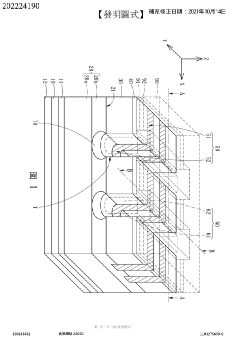
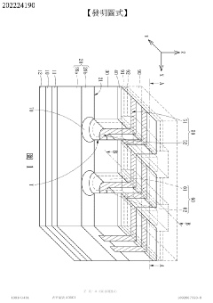
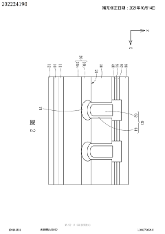
Silicon carbide semiconductor device particular relating to a trenched silicon carbide metal-oxide-semiconductor field-effect transistor (MOSFET)
PatentActiveTW202224190A
Innovation
- A trench-type silicon carbide metal-oxide-semiconductor field-effect transistor (MOSFET) structure is designed with a specific layout and doping concentrations, incorporating a field plate and shielding region to enhance electron depletion and reduce on-resistance, along with a gate insulating layer and complex gate structure for faster switching.

Material Science Advancements for SiC Packaging
Recent advancements in material science have significantly contributed to addressing the thermal management challenges in SiC MOSFET packaging. Traditional packaging materials often fail to adequately handle the high-temperature operation capabilities of SiC devices, which can function efficiently at temperatures exceeding 200°C. This has necessitated the development of novel materials with enhanced thermal conductivity, improved mechanical stability, and better coefficient of thermal expansion (CTE) matching.
High thermal conductivity ceramics, such as aluminum nitride (AlN) and silicon nitride (Si3N4), have emerged as promising substrate materials for SiC packaging. These materials offer thermal conductivity values of 170-230 W/m·K and 70-90 W/m·K respectively, significantly outperforming conventional alumina (Al2O3) substrates with thermal conductivity of approximately 24-28 W/m·K. The improved thermal performance allows for more efficient heat dissipation from SiC MOSFETs during high-power operation.
Advanced die-attach materials represent another critical area of development. Silver sintering technology has gained prominence as a replacement for traditional solder materials, offering thermal conductivity exceeding 200 W/m·K compared to conventional lead-free solders (50-70 W/m·K). Additionally, transient liquid phase bonding (TLPB) materials provide excellent thermal stability and reliability at elevated temperatures, addressing the thermal cycling challenges inherent in SiC applications.
Encapsulation materials have also evolved to meet SiC thermal requirements. High-temperature silicones and epoxy molding compounds with glass transition temperatures above 200°C have been developed specifically for SiC packaging. These materials incorporate ceramic fillers like boron nitride and aluminum oxide to enhance thermal conductivity while maintaining electrical insulation properties. Some advanced formulations achieve thermal conductivity values of 3-5 W/m·K, representing a 5-10x improvement over standard encapsulants.
Thermal interface materials (TIMs) have seen significant innovation with the introduction of phase-change materials, graphene-enhanced compounds, and metal-matrix composites. These next-generation TIMs offer thermal conductivity values ranging from 5 W/m·K to over 20 W/m·K, dramatically reducing thermal resistance at critical interfaces within SiC packages. Carbon-based additives, particularly carbon nanotubes and graphene, have demonstrated particular promise in creating thermally conductive pathways while maintaining compliance.
Metallization systems for SiC devices have progressed beyond traditional aluminum to incorporate materials with superior electromigration resistance and thermal stability. Multi-layer metallization schemes utilizing titanium, nickel, silver, and gold have been optimized specifically for high-temperature SiC operation, ensuring reliable electrical and thermal connections even under extreme thermal cycling conditions.
Reliability Testing Standards for High-Temperature SiC Applications
Reliability testing standards for SiC MOSFETs operating in high-temperature environments have evolved significantly to address the unique thermal challenges these devices face. The Joint Electron Device Engineering Council (JEDEC) has established several key standards specifically for wide bandgap semiconductors, including JEP180 and JC-70, which outline testing methodologies for SiC power devices under thermal stress conditions. These standards define specific temperature cycling tests, high-temperature operating life (HTOL) tests, and temperature-humidity-bias (THB) tests tailored to the extended temperature ranges of SiC devices.
The Automotive Electronics Council (AEC) has also developed the AEC-Q101 qualification standard, which has been adapted to accommodate the higher temperature capabilities of SiC MOSFETs. This adaptation includes more stringent requirements for high-temperature reverse bias (HTRB) testing, typically conducted at temperatures exceeding 150°C for SiC devices compared to the 125°C standard for silicon devices.
Military and aerospace applications have even more demanding standards, with MIL-STD-750 and MIL-STD-883 providing test methods for semiconductor devices that must operate reliably in extreme environments. These standards have been updated to include specific provisions for SiC devices, requiring operational stability at temperatures up to 300°C in some cases.
Thermal cycling reliability tests for SiC MOSFETs typically involve temperature excursions from -55°C to +175°C or higher, with dwell times designed to stress the package-die interface. The number of cycles has been increased in many standards to account for the higher thermal expansion coefficient mismatches in SiC packaging materials.
Power cycling tests have also been modified to reflect the faster switching capabilities and higher power densities of SiC devices. These tests now often include measurement of thermal impedance changes over time as an early indicator of package degradation or die attach deterioration.
Accelerated life testing methodologies have been refined to better correlate with actual field reliability for SiC devices. The Arrhenius equation parameters have been adjusted to account for the different activation energies associated with SiC failure mechanisms compared to silicon devices. This has led to the development of new acceleration factors specific to SiC technology.
International standards organizations such as IEC have also contributed to the standardization landscape with IEC 60747-9 and IEC 60749 series, which now include specific considerations for SiC power devices. These standards emphasize the importance of gate oxide reliability testing, as this remains one of the critical reliability concerns for SiC MOSFETs at elevated temperatures.
Unlock deeper insights with Patsnap Eureka Quick Research — get a full tech report to explore trends and direct your research. Try now!
Generate Your Research Report Instantly with AI Agent
Supercharge your innovation with Patsnap Eureka AI Agent Platform!