Design Strategies For EMI Reduction In SiC MOSFET Circuits
SEP 5, 202510 MIN READ
Generate Your Research Report Instantly with AI Agent
Patsnap Eureka helps you evaluate technical feasibility & market potential.
SiC MOSFET EMI Challenges and Objectives
Silicon Carbide (SiC) MOSFET technology has emerged as a revolutionary advancement in power electronics over the past decade, offering superior performance characteristics compared to traditional silicon-based devices. The evolution of this technology has been driven by increasing demands for higher efficiency, power density, and reliability in power conversion systems across various industries including automotive, renewable energy, and industrial applications.
SiC MOSFETs provide significant advantages including higher breakdown voltage, faster switching speeds, lower on-resistance, and better thermal conductivity. These properties enable operation at higher temperatures, frequencies, and voltages while maintaining efficiency. However, these same characteristics that make SiC MOSFETs attractive also introduce significant electromagnetic interference (EMI) challenges that must be addressed for successful implementation.
The rapid switching transitions (high dv/dt and di/dt) inherent to SiC MOSFETs generate substantial electromagnetic noise across a wide frequency spectrum. This noise can compromise the functionality of nearby electronic systems, violate electromagnetic compatibility (EMC) standards, and reduce overall system reliability. As switching frequencies continue to increase to maximize the benefits of SiC technology, EMI issues become increasingly problematic.
Industry trends indicate a growing adoption of SiC technology, with the market expected to expand at a CAGR of over 30% through 2026. This growth trajectory necessitates concurrent advancements in EMI mitigation strategies to ensure compliance with increasingly stringent regulatory standards such as CISPR, FCC, and automotive EMC requirements.
The primary technical objective in this domain is to develop comprehensive design strategies that effectively reduce EMI in SiC MOSFET circuits without significantly compromising their performance advantages. This includes optimizing gate drive designs, implementing advanced PCB layout techniques, developing innovative filtering solutions, and exploring active EMI cancellation methods.
Secondary objectives include quantifying the EMI generation mechanisms specific to SiC technology, establishing standardized testing methodologies for SiC-based power converters, and developing predictive models that can accurately simulate EMI behavior during the design phase to reduce development cycles.
The convergence of wide bandgap semiconductor physics, power electronics, electromagnetic theory, and system design principles makes this a multidisciplinary challenge requiring integrated approaches. Recent research indicates that addressing EMI issues at multiple levels—semiconductor design, packaging, circuit layout, and system integration—yields the most effective results.
As SiC MOSFET technology continues to mature and penetrate new application domains, the development of standardized, cost-effective EMI reduction strategies will be crucial for enabling the technology to reach its full market potential and deliver on its promise of more efficient, compact, and reliable power conversion systems.
Market Demand for Low-EMI SiC Power Electronics
The global market for Silicon Carbide (SiC) power electronics with low electromagnetic interference (EMI) characteristics is experiencing robust growth, driven by increasing adoption across multiple industries. The demand for SiC MOSFETs with reduced EMI has been particularly strong in electric vehicles (EVs), renewable energy systems, industrial drives, and data center power supplies, where high-frequency switching operations and power density requirements are critical.
Electric vehicle manufacturers represent the largest market segment, with automotive power electronics projected to reach $12.7 billion by 2027. These manufacturers are actively seeking SiC solutions that minimize EMI to comply with stringent automotive EMC standards while maximizing power conversion efficiency. The automotive sector's transition toward 800V and higher voltage platforms has further accelerated the need for SiC MOSFETs with superior EMI performance.
Renewable energy applications constitute another significant market, with solar inverters and wind power converters increasingly adopting SiC technology. The market for SiC in renewable energy applications is growing at 25% annually, with EMI reduction being a key purchasing criterion as these systems must operate in grid-connected environments without causing electromagnetic disturbances.
Industrial motor drives represent a mature but expanding market for low-EMI SiC solutions, valued at approximately $3.2 billion. Factory automation and Industry 4.0 initiatives are driving demand for more compact, efficient, and electromagnetically compatible power conversion systems. The industrial sector particularly values SiC solutions that can reduce or eliminate the need for bulky EMI filters.
Data center power supplies have emerged as a high-growth segment, with efficiency and power density requirements driving SiC adoption. This market segment is expected to grow at 30% annually through 2026, with EMI considerations becoming increasingly important as data centers pack more computing power into limited spaces.
Regional analysis indicates that Asia-Pacific currently leads the market demand, accounting for 45% of global consumption, followed by North America (28%) and Europe (22%). China's aggressive push toward electrification has created substantial demand for SiC power electronics with low EMI characteristics.
Market research indicates that customers are willing to pay a premium of 15-20% for SiC solutions with demonstrably superior EMI performance, as this reduces system-level costs by minimizing filtering requirements and simplifying compliance certification processes. This premium pricing opportunity represents a significant value proposition for manufacturers who can effectively address EMI challenges in their SiC MOSFET designs.
The market is increasingly demanding integrated solutions that combine SiC MOSFETs with optimized gate drivers and EMI mitigation features, rather than discrete components that require extensive system-level engineering to address EMI concerns.
Current EMI Mitigation Techniques and Limitations
Current EMI mitigation techniques for SiC MOSFET circuits can be categorized into three main approaches: circuit design optimization, component selection and placement, and shielding/filtering strategies. Each approach offers specific advantages but also presents inherent limitations that must be addressed in high-frequency, high-power density applications.
Circuit design optimization techniques include gate drive optimization, which involves careful tuning of gate resistance values and implementing dual-path gate drivers to balance switching speed with EMI generation. While effective, this approach often creates trade-offs between switching losses and EMI performance. Another technique is layout optimization, where minimizing loop areas and parasitic inductances can significantly reduce EMI. However, thermal management requirements and physical constraints in power modules often limit the extent of possible layout improvements.
Soft-switching topologies represent another significant mitigation strategy, employing zero-voltage switching (ZVS) or zero-current switching (ZCS) to reduce di/dt and dv/dt rates. These techniques effectively decrease EMI generation but typically increase system complexity and may reduce overall efficiency in certain operating conditions, particularly at light loads.
Component selection plays a crucial role in EMI mitigation, with snubber circuits being widely implemented to suppress voltage spikes and ringing. Traditional RC and RCD snubbers, while effective, introduce additional power losses that can be particularly problematic in high-efficiency SiC applications. Common mode chokes and EMI filters are extensively used but add volume, weight, and cost to the system, potentially negating some of the size advantages offered by SiC technology.
Shielding techniques, including proper grounding strategies and Faraday shields, provide protection against radiated emissions but add manufacturing complexity and cost. The effectiveness of these approaches diminishes at the very high frequencies characteristic of SiC switching transients, often exceeding 100 MHz.
A significant limitation across all current mitigation techniques is their reactive rather than predictive nature. Most approaches address EMI after it has been generated rather than preventing its creation. Additionally, traditional EMI mitigation methods developed for silicon-based power electronics often prove inadequate for SiC MOSFETs due to their fundamentally different switching characteristics and higher operating frequencies.
The trade-off between switching speed and EMI remains a fundamental challenge. Techniques that reduce EMI by slowing switching transitions directly impact the efficiency benefits that make SiC MOSFETs attractive. This creates a complex optimization problem that current solutions address only partially, highlighting the need for more integrated approaches that consider EMI mitigation from the earliest stages of circuit design.
Established EMI Suppression Methods for SiC MOSFET Circuits
01 Gate driver circuit design for EMI reduction
Specialized gate driver circuits can significantly reduce electromagnetic interference in SiC MOSFET applications. These designs control the switching behavior by optimizing gate resistance, implementing multi-stage turn-on/off processes, and utilizing advanced gate drive topologies. By controlling the slew rate and switching transitions, these circuits minimize voltage and current oscillations that contribute to EMI, while maintaining the high-speed switching advantages of SiC MOSFETs.- Gate driver circuit optimization for EMI reduction: Optimizing gate driver circuits in SiC MOSFET applications can significantly reduce electromagnetic interference. Techniques include controlling gate resistance, implementing multi-stage turn-on/off profiles, and using advanced gate driver ICs with precise timing control. These methods help manage the high switching speeds of SiC MOSFETs while minimizing voltage overshoot and ringing that contribute to EMI emissions.
- Filter and layout design techniques: Proper filter design and PCB layout techniques are crucial for EMI reduction in SiC MOSFET circuits. This includes implementing common-mode and differential-mode filters, strategic placement of decoupling capacitors, minimizing loop areas, and using ground planes effectively. Careful consideration of component placement and routing can significantly reduce parasitic inductances that contribute to EMI generation.
- Soft-switching and resonant circuit topologies: Implementing soft-switching techniques and resonant circuit topologies can substantially reduce EMI in SiC MOSFET applications. These approaches minimize switching losses and reduce the high dv/dt and di/dt rates associated with hard-switching, which are major sources of EMI. Zero-voltage switching (ZVS) and zero-current switching (ZCS) techniques help create smoother transitions during switching events.
- Advanced packaging and shielding methods: Advanced packaging and shielding methods can effectively contain and reduce EMI in SiC MOSFET circuits. These include using EMI-absorbing materials, implementing proper shielding enclosures, and employing advanced module packaging techniques that minimize parasitic elements. Integrated cooling solutions that also provide EMI shielding offer dual benefits for high-power SiC applications.
- Modulation and control strategies: Specialized modulation and control strategies can be employed to reduce EMI in SiC MOSFET-based power converters. These include spread spectrum techniques that distribute EMI energy across a wider frequency range, random or variable switching frequency methods, and advanced PWM schemes. Active EMI cancellation techniques can also be implemented to counteract specific EMI frequencies generated during operation.
02 Filter and layout optimization techniques
Proper filter design and PCB layout optimization are critical for EMI reduction in SiC MOSFET circuits. This includes implementing common-mode and differential-mode filters, strategic placement of decoupling capacitors, and minimizing parasitic inductances through optimized trace routing. Advanced PCB layout techniques such as Kelvin source connections, symmetrical power loop designs, and careful component placement help contain high-frequency noise generated during fast switching transitions.Expand Specific Solutions03 Soft-switching and resonant topologies
Implementing soft-switching techniques and resonant circuit topologies can substantially reduce EMI in SiC MOSFET applications. These approaches ensure that switching occurs at zero voltage or zero current conditions, minimizing the high dv/dt and di/dt transients that generate electromagnetic noise. Resonant converters, quasi-resonant circuits, and active auxiliary circuits that facilitate soft-switching can be integrated with SiC MOSFETs to maintain high efficiency while reducing conducted and radiated emissions.Expand Specific Solutions04 Advanced packaging and shielding methods
Innovative packaging and shielding techniques specifically designed for SiC MOSFET applications can effectively contain EMI. These include low-inductance module designs, integrated EMI shields within the package, and advanced thermal management solutions that also serve as electromagnetic shields. Specialized encapsulation materials with EMI-absorbing properties and strategic placement of shielding structures around critical circuit components help prevent radiation of electromagnetic noise while maintaining the thermal performance needed for SiC devices.Expand Specific Solutions05 Active EMI suppression techniques
Active EMI suppression methods employ additional circuitry to counteract electromagnetic interference generated by SiC MOSFET switching. These techniques include active filters that dynamically respond to noise signatures, noise cancellation circuits that generate opposing signals to neutralize EMI, and adaptive control algorithms that modify switching patterns to minimize harmonic content. By actively monitoring and responding to EMI in real-time, these approaches can achieve superior noise reduction compared to passive methods alone.Expand Specific Solutions
Leading Manufacturers and Research Institutions in SiC Technology
The EMI reduction in SiC MOSFET circuits market is in a growth phase, driven by increasing adoption of wide bandgap semiconductors in power electronics. The global market is expanding rapidly, estimated at $1.5-2 billion with projected CAGR of 25-30% through 2028. Technologically, solutions are advancing from basic filtering to integrated approaches. Leading companies like Infineon Technologies demonstrate mature commercial solutions, while Chinese entities such as Yangzhou Yangjie, Suzhou Convert, and Global Power Technology are rapidly developing competitive technologies. Academic institutions including Nanjing University of Aeronautics & Astronautics and University of Electronic Science & Technology of China are contributing significant research innovations, accelerating the transition from laboratory concepts to industrial applications.
Xidian University
Technical Solution: Xidian University has developed innovative EMI reduction strategies for SiC MOSFET circuits through their Electromagnetic Compatibility Research Center. Their approach focuses on comprehensive electromagnetic modeling coupled with novel circuit topologies specifically designed to address the unique challenges of high-frequency SiC switching. Xidian researchers have pioneered advanced gate drive architectures incorporating active impedance modulation techniques that can dynamically adjust switching trajectories to minimize EMI generation while maintaining efficiency. Their work includes specialized common-mode noise suppression methods using balanced circuit topologies and optimized filter structures that have demonstrated up to 30dB reduction in critical frequency bands. Xidian has also developed novel spread spectrum modulation techniques adapted specifically for SiC power converters, effectively distributing EMI energy across wider frequency bands to reduce peak emissions by 10-15dB. Their research extends to advanced PCB layout optimization using computational electromagnetic modeling to identify and mitigate parasitic coupling paths. Additionally, Xidian has contributed significant work on integrated EMI sensing and closed-loop mitigation strategies that adaptively respond to changing operating conditions.
Strengths: Strong theoretical foundation in electromagnetic compatibility; innovative spread spectrum techniques specifically adapted for SiC applications; advanced modeling capabilities for parasitic effects. Weaknesses: Some solutions remain primarily in research phase; higher computational requirements for implementation of advanced techniques; limited industrial validation of some proposed methods.
Huazhong University of Science & Technology
Technical Solution: Huazhong University of Science & Technology (HUST) has developed sophisticated EMI reduction strategies for SiC MOSFET circuits through their Power Electronics and Motor Drive Laboratory. Their approach centers on multi-physics modeling that integrates electromagnetic, thermal, and electrical domains to comprehensively address EMI challenges. HUST researchers have pioneered advanced gate drive architectures with active Miller clamp circuits that effectively suppress voltage oscillations during switching transitions, reducing high-frequency emissions by up to 15dB. Their work includes innovative power loop designs that implement distributed DC-link capacitor networks strategically placed to minimize parasitic inductances to below 5nH in some configurations. HUST has also developed specialized EMI filter topologies optimized specifically for SiC MOSFET characteristics, incorporating novel magnetic materials and winding structures that provide superior attenuation in the 10-50MHz range where SiC devices typically generate significant emissions. Additionally, their research includes advanced PCB layout techniques using segmented power planes and optimized ground return paths to minimize common-mode current generation.
Strengths: Comprehensive multi-physics approach to EMI modeling and mitigation; innovative filter designs specifically optimized for SiC applications; strong integration of theoretical and experimental validation. Weaknesses: Some solutions require specialized manufacturing capabilities; limited commercial implementation examples; higher complexity in design implementation.
Critical Patents and Innovations in SiC EMI Reduction
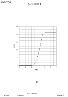
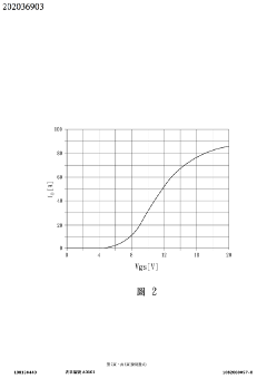
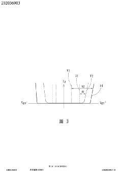
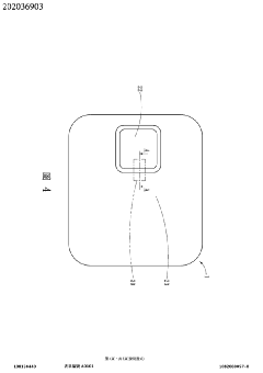
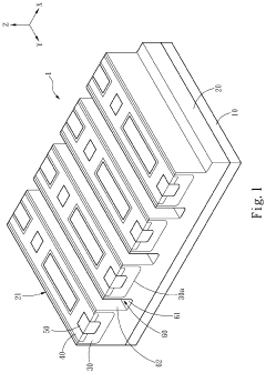
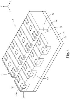
Silicon carbide semiconductor device integrating clamper circuit for clamping voltage
PatentActiveTW202036903A
Innovation
- Integration of a bidirectional voltage clamp with a silicon carbide semiconductor device, comprising a metal oxide semiconductor field effect transistor and p-type floating regions, to suppress both positive and negative overvoltages and enhance electrostatic discharge tolerance.
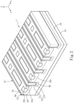
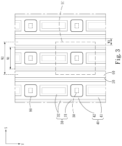
Silicon carbide semiconductor device
PatentPendingUS20240234569A9
Innovation
- A silicon carbide semiconductor device with a hybrid gate structure featuring a trench gate configuration that reduces JFET resistance and parasitic gate-to-drain capacitance, enhancing switching performance by increasing channel width density and optimizing the layout of doped regions and trenches.
Regulatory Compliance and EMC Standards for SiC Applications
The regulatory landscape for Silicon Carbide (SiC) MOSFET applications continues to evolve as these high-performance devices gain wider adoption across industries. Compliance with Electromagnetic Compatibility (EMC) standards is particularly critical for SiC MOSFET circuits due to their inherently faster switching speeds and higher dv/dt and di/dt characteristics, which can generate significant electromagnetic interference (EMI).
International standards such as IEC 61000 series provide comprehensive frameworks for EMC compliance, with specific parts addressing emission limits (IEC 61000-3) and immunity requirements (IEC 61000-4). For SiC applications in power electronics, CISPR 11 (for industrial, scientific, and medical equipment) and CISPR 22/32 (for information technology equipment) establish crucial conducted and radiated emission limits that must be adhered to during product development.
Regional variations in EMC regulations present additional challenges for global deployment of SiC-based systems. The European Union enforces the EMC Directive 2014/30/EU, requiring CE marking for products sold within its borders. In North America, FCC Part 15 governs unintentional radiators, while automotive applications must comply with CISPR 25 and ISO 11452 standards, which are particularly stringent due to the dense electronic environment in modern vehicles.
The unique characteristics of SiC MOSFETs necessitate special consideration when designing for regulatory compliance. The higher switching frequencies enabled by SiC technology often push emissions into frequency ranges where traditional silicon-based systems rarely operated, requiring more sophisticated filtering and shielding solutions. Testing methodologies must also adapt to accurately capture the high-frequency components generated by SiC switching transients.
Pre-compliance testing has become increasingly important in SiC-based design workflows, allowing engineers to identify potential EMI issues early in the development cycle. This approach typically involves near-field scanning, conducted emission pre-testing, and radiated emission assessments in semi-anechoic environments before formal certification testing.
Recent trends in regulatory frameworks show movement toward harmonization of standards across regions and industries, potentially simplifying compliance processes for manufacturers. However, this is counterbalanced by increasingly stringent limits being introduced as electronic device density increases in modern applications. SiC MOSFET circuit designers must therefore maintain awareness of both current requirements and emerging regulatory developments.
Successful EMC compliance strategies for SiC applications typically involve a combination of circuit layout optimization, appropriate gate driver selection, optimized switching trajectories, and carefully designed filtering components. Documentation of compliance testing and certification represents a significant aspect of product development, with comprehensive test reports required to demonstrate conformity with applicable standards.
Thermal Management Considerations in EMI-Optimized SiC Circuits
Thermal management in SiC MOSFET circuits presents unique challenges when optimizing for EMI reduction, as these two aspects are intrinsically interconnected. The high switching speeds that make SiC devices attractive also generate significant heat and contribute to EMI issues. Effective thermal management strategies must therefore be designed with EMI considerations in mind.
The thermal characteristics of SiC MOSFETs differ significantly from traditional silicon devices. SiC can operate at junction temperatures up to 200°C, compared to silicon's typical 150°C limit. However, this higher temperature operation can exacerbate EMI problems by increasing parasitic capacitances and altering device switching behavior.
Heat sink design becomes particularly critical in EMI-optimized circuits. Traditional aluminum heat sinks with fins can act as antennas, radiating EMI if not properly designed. Implementing grounded heat sinks with appropriate shielding can serve dual purposes of thermal management and EMI suppression. Some advanced designs incorporate ferrite materials into heat sink structures to absorb high-frequency emissions while maintaining thermal performance.
Thermal interface materials (TIMs) selection must balance thermal conductivity with electrical isolation properties. Certain ceramic-filled silicone materials offer excellent thermal conductivity while providing electrical isolation that can reduce common-mode noise paths. The thickness and composition of these materials must be carefully selected to optimize both thermal transfer and EMI suppression.
PCB layout strategies for thermal management must complement EMI reduction techniques. Thermal vias, which help dissipate heat from power devices, should be arranged to minimize loop areas and reduce inductive coupling. Strategic placement of thermal copper planes can serve as both heat spreaders and EMI shields when properly connected to ground.
Active cooling solutions introduce additional EMI considerations. Fan-based cooling systems generate electrical noise from motors and can create mechanical vibrations that affect circuit performance. In EMI-sensitive applications, liquid cooling may be preferable despite higher complexity, as it eliminates these noise sources while providing superior thermal performance.
Temperature monitoring and management systems must be designed with awareness of their potential contribution to EMI. Sensor wiring can create antenna effects if improperly routed, while control circuits for thermal management can introduce switching noise. Optical temperature sensing technologies offer advantages in EMI-sensitive environments by eliminating electrical connections.
The relationship between operating temperature and switching characteristics directly impacts EMI generation. As junction temperature increases, switching speeds typically decrease, potentially reducing high-frequency emissions but compromising efficiency. Adaptive gate driving techniques that adjust switching parameters based on temperature can optimize this balance dynamically.
Unlock deeper insights with Patsnap Eureka Quick Research — get a full tech report to explore trends and direct your research. Try now!
Generate Your Research Report Instantly with AI Agent
Supercharge your innovation with Patsnap Eureka AI Agent Platform!