What Are The Roadblocks To Mass Adoption Of SiC MOSFETs?
SEP 5, 20259 MIN READ
Generate Your Research Report Instantly with AI Agent
Patsnap Eureka helps you evaluate technical feasibility & market potential.
SiC MOSFET Evolution and Adoption Goals
Silicon Carbide (SiC) MOSFETs have evolved significantly since their initial development in the early 1990s. The technology has progressed from laboratory curiosities to commercially viable power semiconductor devices that offer substantial advantages over traditional silicon-based alternatives. The evolution trajectory began with rudimentary devices exhibiting high on-resistance and reliability issues, gradually advancing to today's sophisticated components capable of handling high voltages and temperatures while maintaining efficiency.
The technological progression of SiC MOSFETs has been marked by several key milestones. In the early 2000s, researchers overcame critical interface quality challenges that had previously limited device performance. By 2010, the first commercial SiC MOSFETs entered the market, though with limited applications due to cost constraints and reliability concerns. The period between 2015 and 2020 saw dramatic improvements in manufacturing processes, resulting in enhanced yield rates and reduced defect densities.
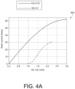
Current generation SiC MOSFETs demonstrate impressive specifications, including breakdown voltages exceeding 1700V, on-resistance values approaching theoretical limits, and switching frequencies far surpassing silicon counterparts. These advancements have positioned SiC technology as a critical enabler for next-generation power electronics systems, particularly in electric vehicles, renewable energy systems, and industrial applications.
The adoption goals for SiC MOSFETs center around several key objectives that must be achieved to facilitate mass market penetration. Primary among these is cost reduction, with industry targets aiming for a 40-50% decrease in production costs over the next five years. This cost trajectory is essential to compete effectively with established silicon technologies and emerging alternatives like gallium nitride (GaN).
Reliability enhancement represents another crucial adoption goal. While current SiC devices demonstrate impressive performance metrics, long-term reliability under extreme operating conditions remains a concern for risk-averse industries like automotive and aerospace. The technology roadmap emphasizes improvements in gate oxide reliability, reduction in threshold voltage drift, and enhanced robustness against short-circuit events.
Manufacturing scalability constitutes the third major adoption goal. Current SiC wafer production faces challenges in scaling to larger diameters comparable to silicon manufacturing. The industry aims to transition from predominantly 6-inch wafers to 8-inch platforms by 2025, with corresponding improvements in defect density and yield rates to support volume production demands.
Standardization efforts represent the final critical adoption goal. As the ecosystem matures, establishing unified standards for testing, qualification, and application-specific performance metrics will accelerate adoption across conservative industries that require predictable, well-characterized components for mission-critical systems.
The technological progression of SiC MOSFETs has been marked by several key milestones. In the early 2000s, researchers overcame critical interface quality challenges that had previously limited device performance. By 2010, the first commercial SiC MOSFETs entered the market, though with limited applications due to cost constraints and reliability concerns. The period between 2015 and 2020 saw dramatic improvements in manufacturing processes, resulting in enhanced yield rates and reduced defect densities.
Current generation SiC MOSFETs demonstrate impressive specifications, including breakdown voltages exceeding 1700V, on-resistance values approaching theoretical limits, and switching frequencies far surpassing silicon counterparts. These advancements have positioned SiC technology as a critical enabler for next-generation power electronics systems, particularly in electric vehicles, renewable energy systems, and industrial applications.
The adoption goals for SiC MOSFETs center around several key objectives that must be achieved to facilitate mass market penetration. Primary among these is cost reduction, with industry targets aiming for a 40-50% decrease in production costs over the next five years. This cost trajectory is essential to compete effectively with established silicon technologies and emerging alternatives like gallium nitride (GaN).
Reliability enhancement represents another crucial adoption goal. While current SiC devices demonstrate impressive performance metrics, long-term reliability under extreme operating conditions remains a concern for risk-averse industries like automotive and aerospace. The technology roadmap emphasizes improvements in gate oxide reliability, reduction in threshold voltage drift, and enhanced robustness against short-circuit events.
Manufacturing scalability constitutes the third major adoption goal. Current SiC wafer production faces challenges in scaling to larger diameters comparable to silicon manufacturing. The industry aims to transition from predominantly 6-inch wafers to 8-inch platforms by 2025, with corresponding improvements in defect density and yield rates to support volume production demands.
Standardization efforts represent the final critical adoption goal. As the ecosystem matures, establishing unified standards for testing, qualification, and application-specific performance metrics will accelerate adoption across conservative industries that require predictable, well-characterized components for mission-critical systems.
Market Demand Analysis for SiC Power Devices
The Silicon Carbide (SiC) power device market is experiencing unprecedented growth, driven primarily by the rapid expansion of electric vehicles (EVs), renewable energy systems, and industrial power applications. Current market analysis indicates that the global SiC power device market reached approximately $1.1 billion in 2022 and is projected to grow at a CAGR of 34% through 2028, potentially reaching $6.5 billion by the end of the forecast period.
Electric vehicle applications represent the largest and fastest-growing segment for SiC MOSFETs, accounting for nearly 60% of the total market demand. This is attributed to the critical need for high-efficiency power conversion in EV powertrains, where SiC devices can increase driving range by 5-10% compared to traditional silicon-based solutions. Major automotive manufacturers have already begun integrating SiC technology into their latest EV models, signaling strong industry confidence in the technology.
The renewable energy sector constitutes the second-largest market for SiC power devices, particularly in solar inverters and wind power systems. The superior switching performance and thermal characteristics of SiC MOSFETs enable higher power density and efficiency in these applications, resulting in smaller system footprints and reduced cooling requirements. Market penetration in this sector has reached approximately 15% and is expected to double within the next five years.
Industrial power applications, including motor drives, uninterruptible power supplies, and data center power systems, represent another significant growth area. These applications benefit from SiC's ability to operate at higher frequencies, which allows for smaller passive components and overall system miniaturization. The industrial segment currently accounts for about 20% of SiC device demand.
Regional analysis reveals that Asia-Pacific dominates the market with approximately 45% share, followed by Europe (30%) and North America (20%). China, in particular, has made significant investments in SiC manufacturing capacity and has implemented favorable policies to accelerate adoption in strategic industries.
Despite positive growth indicators, price sensitivity remains a critical factor affecting market penetration. The cost premium of SiC devices over traditional silicon alternatives currently ranges from 2-5 times, depending on voltage ratings and specifications. However, this gap is narrowing as manufacturing scales up and yields improve. Industry analysts predict that price parity with silicon devices in certain power ranges could be achieved within 7-10 years, which would dramatically accelerate adoption rates.
Customer surveys indicate that beyond price considerations, reliability concerns and limited supplier diversity also influence procurement decisions. As these issues are addressed through continued industry maturation, the adoption curve is expected to steepen significantly in the latter half of this decade.
Technical Barriers and Challenges in SiC MOSFET Development
Despite significant advancements in Silicon Carbide (SiC) MOSFET technology, several critical technical barriers continue to impede its widespread adoption. The most prominent challenge remains the high defect density in SiC wafers, particularly micropipes, dislocations, and basal plane defects. These crystallographic imperfections directly impact device performance and reliability, causing premature failures and inconsistent electrical characteristics across production batches.
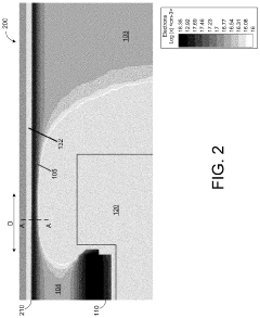
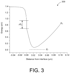
Gate oxide reliability presents another significant hurdle. The interface between SiC and silicon dioxide exhibits substantially higher defect densities compared to traditional silicon devices. This results in reduced channel mobility, threshold voltage instability, and accelerated oxide degradation under high-temperature or high-field conditions, ultimately limiting the operational lifetime of SiC MOSFETs.
Manufacturing scalability continues to constrain mass production capabilities. Current SiC wafer sizes predominantly remain at 6-inch diameter, lagging behind the 12-inch standard in silicon manufacturing. This size limitation, coupled with lower yields and more complex processing requirements, significantly increases production costs. The specialized equipment and modified processes needed for SiC fabrication further complicate integration into existing silicon manufacturing infrastructure.
Thermal management challenges persist despite SiC's inherent thermal conductivity advantages. The higher power densities achievable with SiC MOSFETs create localized hotspots that require advanced packaging solutions. Current packaging technologies struggle to efficiently dissipate heat from these devices, limiting their practical power handling capabilities in real-world applications.
Device characterization and modeling represent additional technical obstacles. Existing simulation models inadequately capture SiC MOSFET behavior across their full operational range, particularly at high temperatures and switching frequencies. This modeling gap complicates circuit design and system integration, forcing engineers to implement excessive design margins that underutilize SiC's performance potential.
Parasitic effects, especially the body diode's poor reverse recovery characteristics and higher forward voltage drop compared to silicon devices, create switching losses that partially offset SiC's efficiency advantages. These parasitic elements become particularly problematic in high-frequency applications where switching losses dominate overall system efficiency.
Long-term reliability data remains insufficient for many mission-critical applications. Accelerated life testing methodologies developed for silicon devices do not accurately predict SiC MOSFET failure mechanisms, creating uncertainty around lifetime expectations in demanding environments like automotive and industrial systems where operational lifespans of 10-15 years are required.
Current Manufacturing Solutions for SiC MOSFETs
01 Manufacturing and fabrication techniques for SiC MOSFETs
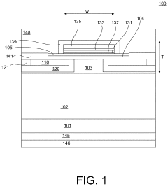
Various manufacturing and fabrication techniques have been developed to enable mass production of Silicon Carbide (SiC) MOSFETs. These techniques focus on improving the quality of the SiC/oxide interface, reducing defects, and enhancing overall device performance. Advanced processes include specialized annealing methods, improved gate oxide formation, and novel doping techniques that collectively contribute to higher yield rates necessary for mass adoption.- Manufacturing and fabrication techniques for SiC MOSFETs: Advanced manufacturing processes have been developed to enable mass production of Silicon Carbide (SiC) MOSFETs. These techniques focus on improving wafer quality, reducing defect density, and optimizing fabrication steps to enhance yield rates. Innovations in epitaxial growth, ion implantation, and annealing processes have contributed to more consistent device performance and reliability, which are critical factors for widespread commercial adoption.
- Power efficiency and thermal management solutions: SiC MOSFETs offer superior power efficiency compared to traditional silicon devices, enabling higher operating temperatures and better thermal management. These advantages make them particularly suitable for high-power applications where energy efficiency is critical. Innovations in packaging technology and cooling systems have been developed specifically for SiC devices to maximize their thermal performance benefits, further supporting their mass adoption in power electronics applications.
- Integration with existing power electronics systems: For mass adoption, SiC MOSFETs must be compatible with existing power electronics infrastructure. Innovations in gate driver design, protection circuits, and control systems have been developed to address the unique characteristics of SiC devices. These solutions enable easier integration into established systems while taking advantage of the superior performance of SiC technology, reducing barriers to adoption across various industries.
- Cost reduction strategies for mass market adoption: High manufacturing costs have been a significant barrier to widespread adoption of SiC MOSFETs. Recent innovations focus on reducing production costs through larger wafer sizes, improved manufacturing yields, and optimized supply chains. Alternative fabrication methods and material processing techniques have been developed to make SiC technology more economically competitive with traditional silicon devices, accelerating market penetration across various applications.
- Application-specific optimizations for emerging markets: To drive mass adoption, SiC MOSFETs are being optimized for specific high-growth applications such as electric vehicles, renewable energy systems, and industrial power supplies. These optimizations include customized device structures, voltage ratings, and switching characteristics tailored to the requirements of each application. By addressing the unique needs of these emerging markets, manufacturers can accelerate the transition from silicon to SiC technology in critical power electronics systems.
02 Power conversion and efficiency improvements
SiC MOSFETs offer significant advantages in power conversion applications due to their superior efficiency compared to traditional silicon devices. These improvements include lower switching losses, higher operating temperatures, and better thermal conductivity. The enhanced performance characteristics enable more compact power conversion systems with higher power density, making SiC MOSFETs particularly attractive for electric vehicles, renewable energy systems, and industrial applications where efficiency is paramount.Expand Specific Solutions03 Circuit design and integration solutions
Specialized circuit designs have been developed to leverage the unique properties of SiC MOSFETs and facilitate their integration into existing systems. These designs address challenges such as high-speed switching, gate drive requirements, and electromagnetic interference mitigation. Advanced packaging technologies and thermal management solutions have also been created to handle the higher power densities and operating temperatures of SiC devices, enabling their broader adoption across various applications.Expand Specific Solutions04 Cost reduction strategies for mass market adoption
Various approaches have been developed to reduce the manufacturing costs of SiC MOSFETs, making them more competitive with traditional silicon devices. These strategies include substrate size increases, process optimization, yield improvements, and economies of scale through higher production volumes. Additionally, innovative material processing techniques and equipment modifications have been implemented to lower the overall production costs while maintaining the superior performance characteristics of SiC devices.Expand Specific Solutions05 Application-specific optimizations for emerging markets
SiC MOSFETs have been specifically optimized for emerging application areas that can benefit from their unique properties. These optimizations include tailored device structures for electric vehicle powertrains, renewable energy inverters, and high-frequency power supplies. By customizing device characteristics such as breakdown voltage, on-resistance, and switching behavior for specific applications, manufacturers have accelerated the adoption of SiC technology in markets where the performance benefits justify the higher initial cost compared to silicon alternatives.Expand Specific Solutions
Key Industry Players in SiC Semiconductor Market
The SiC MOSFET market is currently in a growth phase, transitioning from early adoption to mainstream implementation, with a projected market size exceeding $2 billion by 2025. Despite technical advantages over silicon, mass adoption faces significant roadblocks including high manufacturing costs, packaging challenges, and reliability concerns. Key players demonstrate varying levels of technical maturity: established companies like Power Integrations, NXP, and Mitsubishi Electric lead with commercial solutions, while BYD Semiconductor, BASiC Semiconductor, and GTA Semiconductor are rapidly advancing. Academic institutions including University of Electronic Science & Technology of China and Xidian University contribute significantly to fundamental research. The ecosystem requires further development in standardization, testing protocols, and supply chain optimization to overcome cost barriers and accelerate widespread adoption.
Power Integrations, Inc.
Technical Solution: Power Integrations has developed an innovative approach to SiC MOSFET implementation through their InnoSwitch™ family that integrates SiC MOSFETs with advanced control circuitry. Their technology addresses cost barriers by optimizing SiC usage only where performance benefits justify the premium, while using conventional silicon for peripheral functions. Their manufacturing process incorporates specialized screening techniques to identify and eliminate devices with latent gate oxide defects, significantly improving long-term reliability. Power Integrations has developed proprietary gate driver technology specifically optimized for SiC MOSFETs that addresses the sensitive gate characteristics, providing precise voltage control within ±0.2V tolerance to prevent threshold voltage drift. Their packaging technology features direct bonded copper (DBC) substrates with specialized die-attach materials that accommodate the different thermal expansion coefficients of SiC versus conventional packaging components.
Strengths: Their integrated approach combining SiC with silicon components in optimized packages provides a practical path to adoption by balancing performance gains with cost considerations. Their specialized gate driver technology effectively addresses the sensitive gate oxide issues common in SiC devices. Weaknesses: The hybrid approach, while cost-effective, may not deliver the full performance potential of pure SiC solutions in extremely high-power applications where maximum efficiency is required regardless of cost.
Huawei Digital Power Technologies Co Ltd
Technical Solution: Huawei Digital Power has developed a comprehensive SiC MOSFET technology platform specifically targeting power conversion applications. Their approach focuses on addressing the key roadblocks through vertical integration of the supply chain and specialized manufacturing processes. Huawei has invested in proprietary substrate processing techniques that reduce micropipe defects by over 40% compared to industry standards, significantly improving yield and reliability. Their gate oxide formation process employs a multi-step oxidation technique with precise temperature control (±2°C) throughout the process, reducing interface trap density to below 3×10¹¹ cm⁻² and improving threshold voltage stability. Huawei has also developed specialized packaging solutions with silver-sintering die-attach materials that provide superior thermal performance (thermal resistance reduced by approximately 30%) compared to conventional soldering methods, addressing the thermal management challenges of SiC devices.
Strengths: Vertical integration gives Huawei greater control over the entire manufacturing process, allowing for specialized optimizations at each step. Their advanced packaging technology effectively addresses thermal management challenges critical for SiC device reliability. Weaknesses: As a relatively new entrant to the SiC semiconductor manufacturing space compared to established players, Huawei may face challenges in achieving competitive manufacturing yields and cost structures in the short term.
Critical Patents and Innovations in SiC Technology
Semiconductor device provided by silicon carbide substrate and method for manufacturing the same
PatentInactiveUS20070102708A1
Innovation
- A semiconductor device is designed with a single silicon carbide substrate integrating a vertical type junction field effect transistor (V-JFET) and a lateral type junction field effect transistor (L-JFET), where the drain of the L-JFET connects to the source of the V-JFET, and both share a common gate, allowing for a simplified structure and reduced conduction loss, enabling high temperature operation and low manufacturing costs.
Silicon carbide field-effect transistors
PatentActiveUS20220013661A1
Innovation
- A silicon carbide (SiC) metal-oxide-semiconductor field-effect transistor (MOSFET) design incorporating a substrate, drift region, spreading layer, body region, and source region with a gate structure that includes a gate oxide layer, aluminum nitride, and p-type gallium nitride layers, achieving low on-state specific resistance and high threshold voltage.
Cost-Performance Analysis of SiC vs Silicon Technologies
The economic comparison between Silicon Carbide (SiC) and traditional silicon technologies reveals significant cost-performance trade-offs that directly impact the mass adoption of SiC MOSFETs. Currently, SiC devices command a premium price point approximately 3-5 times higher than their silicon counterparts, primarily due to substrate costs, manufacturing complexity, and lower production volumes. This substantial price differential represents one of the most significant barriers to widespread implementation across cost-sensitive applications.
When evaluating total system costs, however, SiC technologies demonstrate compelling advantages that partially offset their higher initial component costs. The superior thermal conductivity of SiC (approximately 3 times that of silicon) enables simplified cooling systems, while higher switching frequencies allow for smaller passive components. These factors contribute to an estimated 15-30% reduction in overall system size and weight, particularly beneficial in automotive and industrial applications where space constraints are critical.
Performance metrics further illuminate the value proposition of SiC MOSFETs. Their ability to operate at junction temperatures exceeding 200°C (compared to silicon's typical 150°C limit) and withstand higher breakdown voltages (1200V-1700V as standard offerings) delivers tangible efficiency improvements. System-level efficiency gains of 2-5% have been documented across various applications, with particularly impressive results in electric vehicle inverters and solar inverters where efficiency improvements directly translate to extended range or increased energy harvest.
The economic equation becomes more favorable when considering operational lifetime costs. SiC-based systems demonstrate enhanced reliability under thermal cycling and high-temperature operation, potentially extending service intervals and reducing maintenance expenses. Energy savings from improved efficiency compound over the operational lifetime, with calculations indicating potential energy cost reductions of 3-7% in industrial motor drives and 5-10% in power conversion systems.
Market analysis indicates a steadily improving cost trajectory for SiC technologies, with prices declining approximately 10-15% annually as manufacturing scales and yields improve. This trend suggests a crossover point where the total cost of ownership for SiC solutions will achieve parity with silicon alternatives in an expanding range of applications within the next 3-5 years, beginning with high-performance segments where efficiency and size premiums command the greatest value.
The cost-performance equation varies significantly across application segments. In electric vehicles, where battery costs remain substantial and efficiency directly impacts range, the value proposition for SiC is already compelling despite higher initial costs. Conversely, in consumer electronics and low-power applications, the performance benefits may not yet justify the price premium, explaining the segmented adoption patterns observed in the market.
Supply Chain Constraints and Material Availability Issues
The silicon carbide (SiC) MOSFET market faces significant supply chain constraints that currently impede widespread adoption. Raw material availability represents a fundamental challenge, as high-quality SiC substrates require specialized manufacturing processes involving carbon and silicon crystallization under extreme temperatures. The limited number of suppliers capable of producing these substrates to semiconductor-grade specifications creates bottlenecks in the production pipeline, with current global capacity unable to meet rapidly growing demand.
Manufacturing complexity further exacerbates supply issues. The production of SiC wafers involves sophisticated processes including chemical vapor deposition and high-temperature annealing, requiring specialized equipment and expertise. Current manufacturing yields remain lower than those of traditional silicon technologies, with defect densities and process variations contributing to higher costs and limited availability. The industry's reliance on 4-inch and 6-inch wafer production, rather than the 8-inch or 12-inch standards common in silicon manufacturing, creates additional inefficiencies.
Geographic concentration of the supply chain presents strategic vulnerabilities. Key SiC material suppliers and manufacturing facilities are concentrated in specific regions, particularly the United States, Japan, and parts of Europe. This concentration creates potential supply disruptions due to geopolitical tensions, trade restrictions, or localized disasters. The COVID-19 pandemic highlighted these vulnerabilities when manufacturing and logistics disruptions significantly impacted SiC component availability.
Scaling challenges persist throughout the value chain. As demand increases, suppliers face difficulties in rapidly expanding production capacity due to the capital-intensive nature of SiC manufacturing facilities. New production lines require substantial investment in specialized equipment and clean room facilities, with lengthy qualification periods before achieving full production capacity. The specialized nature of SiC processing equipment creates additional supply constraints, as equipment manufacturers struggle to meet growing demand.
Vertical integration strategies are emerging as a response to these constraints. Leading power semiconductor companies are increasingly investing in controlling multiple stages of the supply chain, from substrate production to device fabrication. This approach aims to secure material supply and reduce dependencies, but requires significant capital investment and technical expertise across multiple manufacturing domains.
Unlock deeper insights with Patsnap Eureka Quick Research — get a full tech report to explore trends and direct your research. Try now!
Generate Your Research Report Instantly with AI Agent
Supercharge your innovation with Patsnap Eureka AI Agent Platform!