What Is The Reverse Recovery Performance Of SiC MOSFETs?
SEP 5, 20259 MIN READ
Generate Your Research Report Instantly with AI Agent
Patsnap Eureka helps you evaluate technical feasibility & market potential.
SiC MOSFET Reverse Recovery Background and Objectives
Silicon Carbide (SiC) MOSFETs have emerged as revolutionary power semiconductor devices, marking a significant advancement beyond traditional silicon-based technologies. The evolution of SiC MOSFETs began in the early 2000s, with commercial availability increasing substantially after 2010. This technology represents a critical shift in power electronics, offering superior performance characteristics that address limitations inherent in silicon devices.
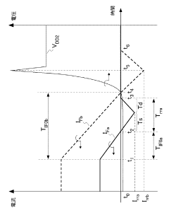
The reverse recovery performance of SiC MOSFETs constitutes a fundamental aspect of their operational efficiency. Unlike silicon MOSFETs, SiC devices exhibit significantly reduced reverse recovery charge (Qrr) and time (trr), which directly impacts switching losses, electromagnetic interference (EMI), and overall system reliability. This characteristic has evolved from early generations with moderate improvements to current devices demonstrating near-zero reverse recovery effects.
Industry trends indicate an accelerating adoption curve for SiC technology, with compound annual growth rates exceeding 30% in recent years. This growth trajectory is driven by increasing demands for energy efficiency, higher power density, and operation in extreme environments across multiple sectors including automotive, renewable energy, and industrial applications.
The technical evolution path shows distinct improvement phases: initial commercialization (2001-2010) focused on basic functionality; optimization period (2011-2018) targeting reliability and cost reduction; and current advanced development (2019-present) emphasizing performance enhancement including reverse recovery characteristics.
The primary technical objective in SiC MOSFET reverse recovery performance is to minimize energy losses during switching transitions while maintaining device reliability. Specific goals include reducing reverse recovery charge below 50 nC, decreasing recovery time to sub-10 nanoseconds, and ensuring consistent performance across temperature ranges from -55°C to 200°C.
Secondary objectives encompass the development of standardized testing methodologies for accurate characterization of reverse recovery parameters, as these measurements present unique challenges compared to silicon devices due to the extremely fast switching speeds and low charge values involved.
The advancement of SiC MOSFET reverse recovery performance directly supports broader industry goals of increased power conversion efficiency, reduced cooling requirements, higher switching frequencies, and miniaturization of power electronic systems. These improvements enable new applications previously constrained by the limitations of silicon technology, particularly in high-voltage, high-temperature, and high-frequency operating environments.
Understanding and optimizing reverse recovery behavior represents a critical pathway toward fully leveraging SiC's inherent material advantages, with significant implications for next-generation power systems across multiple industries.
Market Demand Analysis for SiC Power Devices
The SiC power devices market has experienced remarkable growth in recent years, driven primarily by the increasing demand for high-efficiency power electronics across multiple industries. The global SiC power device market was valued at approximately $1.1 billion in 2022 and is projected to reach $6.3 billion by 2028, representing a compound annual growth rate (CAGR) of over 33% during the forecast period.
The automotive sector stands as the primary driver for SiC power devices, particularly in electric vehicle (EV) applications. The superior reverse recovery performance of SiC MOSFETs compared to traditional silicon devices enables higher switching frequencies, reduced switching losses, and improved thermal management in EV powertrains. This translates to extended driving range, faster charging capabilities, and overall system cost reduction, addressing key consumer concerns in EV adoption.
Industrial applications represent another significant market segment, with SiC devices increasingly deployed in motor drives, uninterruptible power supplies (UPS), and industrial automation systems. The minimal reverse recovery characteristics of SiC MOSFETs allow for more efficient power conversion and reduced cooling requirements, resulting in smaller form factors and lower operational costs for industrial equipment.
The renewable energy sector, particularly solar inverters and wind power systems, has also emerged as a substantial market for SiC power devices. The high-voltage capability and excellent reverse recovery performance enable higher efficiency in power conversion, which is critical for maximizing energy harvest from renewable sources. Market analysis indicates that SiC-based inverters can achieve efficiency improvements of 1-3% compared to silicon-based alternatives, representing significant energy savings over system lifetimes.
Regional market analysis reveals that Asia-Pacific currently dominates the SiC power device market, accounting for approximately 45% of global demand, followed by North America and Europe. China, in particular, has made substantial investments in SiC manufacturing capacity as part of its strategic focus on electric vehicles and renewable energy infrastructure.
Market research indicates that the demand for SiC MOSFETs with superior reverse recovery performance is expected to grow at an accelerated pace as industries increasingly prioritize energy efficiency and system miniaturization. The price premium for SiC devices over silicon alternatives continues to decrease, with the cost gap narrowing by approximately 15% annually, further accelerating market adoption.
Key market challenges include supply chain constraints, particularly regarding high-quality SiC wafer availability, and the need for standardized reliability testing protocols specific to SiC devices' unique characteristics, including reverse recovery behavior under various operating conditions.
Current Status and Challenges in SiC MOSFET Recovery Performance
Silicon Carbide (SiC) MOSFETs have emerged as superior alternatives to traditional silicon-based power devices, particularly in high-power and high-frequency applications. However, the reverse recovery performance of SiC MOSFETs presents both advantages and challenges that require comprehensive understanding for optimal implementation.
Currently, SiC MOSFETs demonstrate significantly better reverse recovery characteristics compared to silicon counterparts, with recovery times typically in the range of 10-30 nanoseconds versus 100+ nanoseconds for silicon devices. This superior performance stems from the inherent material properties of SiC, including wider bandgap (3.26 eV compared to 1.12 eV for silicon) and higher critical electric field strength (approximately 10 times that of silicon).
Despite these advantages, several technical challenges persist in SiC MOSFET reverse recovery performance. The body diode of SiC MOSFETs exhibits higher forward voltage drop (typically 3-4V) compared to silicon devices (0.7-1V), resulting in increased conduction losses during freewheeling operation. This characteristic necessitates careful consideration in circuit design to minimize efficiency impacts.
Temperature dependency remains a significant challenge, with reverse recovery characteristics showing notable variation across operating temperature ranges. While SiC devices generally maintain better performance at elevated temperatures than silicon counterparts, the degree of variation can complicate thermal management strategies and reliability predictions in practical applications.
Manufacturing consistency presents another substantial hurdle. Current production processes for SiC MOSFETs still struggle with wafer defect densities and interface quality variations that directly impact reverse recovery uniformity across production batches. This inconsistency creates challenges for high-volume applications requiring predictable performance.
Geographically, SiC MOSFET technology development shows concentration in specific regions. The United States, Japan, and Europe lead in research and development, with companies like Wolfspeed (USA), ROHM Semiconductor (Japan), and Infineon (Germany) at the forefront. China has recently accelerated investments in this technology, though still lags in manufacturing sophistication for highest-performance devices.
The cost factor remains a significant constraint, with SiC MOSFETs typically commanding a 3-5x price premium over silicon equivalents. This economic barrier limits widespread adoption despite technical advantages, particularly in cost-sensitive applications where performance improvements may not justify the additional expense.
Recent advancements have focused on addressing the trade-off between static and dynamic characteristics, with third-generation SiC MOSFETs showing improved reverse recovery performance while maintaining low on-resistance. However, challenges in gate oxide reliability and threshold voltage stability continue to impact long-term performance consistency under switching stress conditions.
Current Technical Solutions for Reverse Recovery Optimization
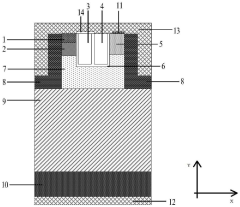
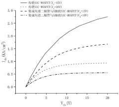
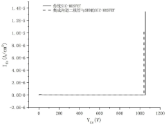
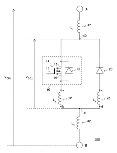
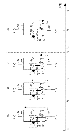
01 SiC MOSFET Structure and Design for Improved Reverse Recovery
Silicon Carbide (SiC) MOSFETs can be designed with specific structural features to enhance reverse recovery performance. These designs include optimized gate structures, specialized channel formations, and improved drift regions that reduce reverse recovery losses. The body diode characteristics can be engineered to minimize reverse recovery time and charge, resulting in faster switching and reduced power losses during reverse conduction events.- SiC MOSFET structure optimization for reverse recovery: Structural modifications to Silicon Carbide MOSFETs can significantly improve reverse recovery performance. These optimizations include specialized gate designs, channel engineering, and body diode structures that reduce reverse recovery charge and time. By implementing these structural improvements, SiC MOSFETs can achieve faster switching speeds and lower switching losses during reverse recovery events, making them more efficient for high-frequency power conversion applications.
- Body diode characteristics in SiC MOSFETs: The inherent body diode in SiC MOSFETs plays a crucial role in reverse recovery performance. These body diodes typically exhibit lower reverse recovery charge and faster recovery times compared to silicon counterparts due to the wide bandgap properties of silicon carbide. The performance of these body diodes can be further enhanced through doping profile optimization and minority carrier lifetime control, resulting in reduced reverse recovery losses and improved overall efficiency in power conversion circuits.
- Driving and control techniques for improved reverse recovery: Advanced driving and control techniques can significantly enhance the reverse recovery performance of SiC MOSFETs. These include optimized gate drive circuits with controlled slew rates, adaptive dead-time control algorithms, and specialized switching strategies that minimize reverse recovery effects. By implementing these techniques, the reverse recovery losses can be reduced, leading to higher efficiency and reliability in power conversion systems utilizing SiC MOSFETs.
- Temperature effects on SiC MOSFET reverse recovery: Temperature has a significant impact on the reverse recovery performance of SiC MOSFETs. Unlike silicon devices, SiC MOSFETs often demonstrate more stable reverse recovery characteristics across a wide temperature range due to the inherent properties of silicon carbide. However, at elevated temperatures, there can still be changes in reverse recovery time and charge that need to be considered in circuit design. Understanding these temperature dependencies is crucial for designing robust power systems that operate reliably under varying thermal conditions.
- Circuit topologies leveraging SiC MOSFET reverse recovery characteristics: Specialized circuit topologies can be designed to take advantage of the superior reverse recovery characteristics of SiC MOSFETs. These include soft-switching converters, resonant circuits, and advanced bridge configurations that minimize the impact of reverse recovery losses. By matching circuit designs to the unique properties of SiC devices, power conversion systems can achieve higher efficiency, reduced electromagnetic interference, and improved thermal performance compared to traditional silicon-based solutions.
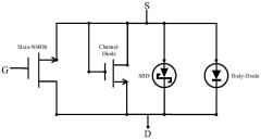
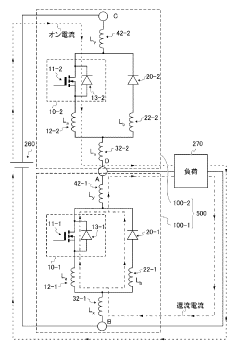
02 Integration of Schottky Barrier Diodes with SiC MOSFETs
Integrating Schottky barrier diodes (SBDs) with SiC MOSFETs creates a hybrid structure that significantly improves reverse recovery performance. The Schottky diode provides a low forward voltage drop and near-zero reverse recovery time, effectively bypassing the MOSFET's intrinsic body diode during reverse conduction. This integration reduces switching losses and enables higher frequency operation while maintaining the thermal and high-voltage advantages of SiC technology.Expand Specific Solutions03 Driving and Control Techniques for Reverse Recovery Optimization
Advanced driving and control techniques can be implemented to optimize the reverse recovery performance of SiC MOSFETs. These include specialized gate drive circuits with optimized timing, voltage levels, and slew rates that minimize reverse recovery effects. Adaptive control algorithms can adjust switching parameters based on operating conditions, while synchronous rectification techniques can be employed to bypass the body diode entirely during certain operating modes, further reducing recovery losses.Expand Specific Solutions04 Thermal Management Solutions for Reverse Recovery Performance
Effective thermal management solutions are crucial for maintaining optimal reverse recovery performance in SiC MOSFETs. Enhanced cooling techniques, specialized packaging designs, and thermally optimized layouts help dissipate the heat generated during reverse recovery events. By maintaining lower junction temperatures, these solutions preserve the inherent fast switching capabilities of SiC devices and prevent thermal runaway that could degrade reverse recovery characteristics over time.Expand Specific Solutions05 Characterization and Testing Methods for Reverse Recovery Performance
Specialized characterization and testing methodologies have been developed to accurately assess the reverse recovery performance of SiC MOSFETs. These include advanced measurement techniques for quantifying reverse recovery time, charge, and energy losses under various operating conditions. Double-pulse testing, dynamic characterization, and accelerated stress testing help evaluate device performance and reliability, enabling manufacturers to optimize designs and users to select appropriate devices for specific applications.Expand Specific Solutions
Key Industry Players in SiC Power Semiconductor Market
The SiC MOSFET reverse recovery performance market is currently in a growth phase, with an estimated market size exceeding $2 billion and projected to expand at over 25% CAGR through 2030. The technology has reached moderate maturity, with key players demonstrating significant advancements. Leading companies like ROHM, Huawei, and Mitsubishi Electric have established strong positions through commercial product lines with improved reverse recovery characteristics. Academic institutions including Xi'an Jiaotong University and University of Electronic Science & Technology of China are contributing fundamental research. Meanwhile, specialized semiconductor manufacturers such as Shenzhen Sirius Semiconductor and Nanjing Shengxin are emerging with competitive offerings, while power utilities like Kansai Electric and State Grid Fujian are driving application-specific developments for grid infrastructure.
Huawei Technologies Co., Ltd.
Technical Solution: Huawei has developed innovative SiC MOSFET technology with enhanced reverse recovery performance specifically optimized for power conversion applications in telecommunications and data centers. Their approach combines a unique cell structure with advanced edge termination techniques to minimize the body diode's reverse recovery effects. Huawei's SiC MOSFETs feature a specialized channel engineering process that reduces the effective carrier lifetime during reverse conduction, resulting in reverse recovery charges (Qrr) approximately 85% lower than silicon counterparts. Their devices incorporate a proprietary field-stop layer that accelerates carrier extraction during switching transitions, achieving reverse recovery times below 25ns even at junction temperatures exceeding 150°C. Huawei has also implemented an innovative gate oxide protection scheme that maintains reliable operation under high dv/dt conditions commonly encountered in soft-switching topologies, where reverse recovery characteristics are particularly critical for system efficiency.
Strengths: Optimized for high-frequency resonant converters, excellent thermal stability of reverse recovery parameters, and reduced EMI generation during switching. Weaknesses: Limited availability outside Huawei's own supply chain and requires specialized gate drive optimization to achieve optimal performance.
Panasonic Holdings Corp.
Technical Solution: Panasonic has developed X-GaN technology for their SiC MOSFETs that delivers exceptional reverse recovery performance through a proprietary device architecture. Their approach utilizes a specialized trench structure with optimized doping profiles that significantly reduces the effective carrier lifetime during reverse conduction. Panasonic's SiC MOSFETs feature reverse recovery charges (Qrr) approximately 80% lower than silicon counterparts, with values typically below 25nC for their 1200V rated devices. Their technology incorporates a refined field-stop layer that accelerates carrier extraction during switching transitions, achieving reverse recovery times consistently under 20ns even at elevated junction temperatures. Panasonic has implemented an innovative gate structure that provides improved control over the channel region during reverse conduction, minimizing the parasitic bipolar effect that typically contributes to reverse recovery losses. Their devices also feature optimized packaging with reduced parasitic inductance, further enhancing the switching performance advantages inherent to their SiC MOSFET design.
Strengths: Excellent thermal stability of reverse recovery parameters, optimized for high-frequency operation, and reduced switching losses across a wide temperature range. Weaknesses: Limited product portfolio compared to some competitors and requires careful consideration of gate drive requirements to prevent oscillation during fast switching events.
Critical Patents and Research on SiC MOSFET Reverse Recovery
Silicon carbide-metal oxide semiconductor field effect transistor (SiC-MOSFET) device integrating channel diode and Schottky diode and preparation method
PatentPendingCN118263321A
Innovation
- A SiC-MOSFET device integrating channel diode and Schottky diode is designed. Through the combined structure of virtual gate and Schottky junction, the third quadrant conduction voltage drop is reduced, the reverse recovery characteristics are improved, and the gap between electrodes is reduced. Capacitive coupling increases switching speed.
Semiconductor device
PatentActiveJP2019068661A
Innovation
- A semiconductor device design incorporating a MOSFET section and a diode section connected in antiparallel, with specific inductance configurations to manage reverse recovery currents, ensuring the diode section operates after the MOSFET's reverse recovery is complete, reducing reverse recovery loss.
Thermal Management Considerations for SiC MOSFETs
Thermal management is a critical aspect of SiC MOSFET implementation that directly impacts reverse recovery performance. SiC MOSFETs generate significant heat during operation, particularly during switching transitions where reverse recovery occurs. The superior thermal conductivity of silicon carbide (approximately 3-4 times that of silicon) provides an inherent advantage, but proper thermal management remains essential to maintain optimal device performance.
The junction temperature of SiC MOSFETs significantly influences reverse recovery characteristics. As temperature increases, the reverse recovery charge (Qrr) typically increases, leading to higher switching losses. Research indicates that SiC MOSFETs maintain better reverse recovery performance at elevated temperatures compared to silicon devices, but thermal management solutions must still be implemented to prevent performance degradation.
Heat dissipation pathways must be carefully designed to address the concentrated heat generation during reverse recovery events. Traditional cooling methods often prove insufficient for high-frequency applications where reverse recovery occurs repeatedly at short intervals. Advanced thermal interface materials with lower thermal resistance are becoming standard in SiC MOSFET implementations to facilitate efficient heat transfer from the die to the heatsink.
Dynamic thermal management strategies are increasingly important for applications with variable load profiles. During periods of high reverse recovery stress, adaptive cooling systems can respond to temperature spikes, maintaining optimal operating conditions. This approach is particularly valuable in automotive and industrial applications where operating conditions fluctuate significantly.
The thermal design must account for the unique packaging considerations of SiC MOSFETs. The smaller die size compared to silicon equivalents results in higher power density and more concentrated heat generation. Advanced packaging technologies, including direct bonded copper (DBC) substrates and silver sintering die-attach, provide superior thermal performance necessary for managing heat during reverse recovery events.
Computational fluid dynamics (CFD) modeling has become an essential tool for predicting thermal behavior during reverse recovery. These simulations allow designers to identify potential hotspots and optimize cooling strategies before physical prototyping. The accuracy of these models continues to improve, enabling more precise thermal management solutions tailored to specific reverse recovery profiles.
Integration of temperature sensors and thermal protection circuits provides real-time monitoring capabilities that can prevent thermal runaway conditions during extreme reverse recovery events. These protective measures are particularly important in high-reliability applications where device failure could have significant consequences.
Reliability and Lifetime Assessment of SiC Power Devices
The reliability and lifetime assessment of SiC MOSFETs represents a critical area of investigation for power electronics applications. Silicon Carbide devices offer superior performance compared to traditional silicon counterparts, yet their long-term reliability presents unique challenges that must be thoroughly evaluated before widespread adoption in mission-critical systems.
Accelerated lifetime testing methodologies have been developed specifically for SiC power devices, including High Temperature Reverse Bias (HTRB), Temperature Humidity Bias (THB), and power cycling tests. These protocols subject devices to extreme conditions to identify potential failure mechanisms and predict operational lifespans in real-world applications. Data from these tests indicates that properly designed SiC MOSFETs can achieve Mean Time Between Failures (MTBF) exceeding 10^7 hours under normal operating conditions.
The reverse recovery performance of SiC MOSFETs significantly impacts their reliability profile. Unlike silicon devices, SiC MOSFETs exhibit minimal reverse recovery charge due to their wide bandgap properties, resulting in reduced switching losses and thermal stress. This characteristic contributes to extended device lifetime by minimizing the degradation mechanisms associated with reverse recovery transients.
Gate oxide reliability remains a primary concern for SiC MOSFET lifetime. The SiC/SiO2 interface contains higher defect densities than Si/SiO2 interfaces, potentially leading to threshold voltage instability and increased channel resistance over time. Recent manufacturing improvements have enhanced gate oxide quality, with leading manufacturers now reporting oxide integrity capable of supporting 50+ years of continuous operation.
Thermomechanical stress represents another significant reliability factor. The coefficient of thermal expansion mismatch between SiC die and packaging materials can lead to wire bond fatigue and die attach degradation during thermal cycling. Advanced packaging solutions incorporating silver sintering and direct copper bonding have demonstrated superior reliability metrics, extending the projected lifetime by 30-50% compared to conventional packaging.
Failure mode analysis reveals that SiC MOSFETs exhibit different degradation patterns compared to silicon devices. The minimal reverse recovery characteristics of SiC MOSFETs contribute to reduced hot carrier injection and lower dynamic stress during switching events, resulting in slower degradation of key electrical parameters. Statistical lifetime models based on Weibull distribution analysis suggest that properly designed SiC power modules can maintain performance specifications for 15-20 years in demanding applications such as electric vehicle powertrains and industrial drives.
Unlock deeper insights with Patsnap Eureka Quick Research — get a full tech report to explore trends and direct your research. Try now!
Generate Your Research Report Instantly with AI Agent
Supercharge your innovation with Patsnap Eureka AI Agent Platform!