Evaluate FinFET Design Methods For Improved Yield
SEP 11, 20259 MIN READ
Generate Your Research Report Instantly with AI Agent
Patsnap Eureka helps you evaluate technical feasibility & market potential.
FinFET Evolution and Design Objectives
FinFET technology emerged as a revolutionary advancement in semiconductor manufacturing, evolving from traditional planar MOSFET designs to address the increasing challenges of transistor scaling. The journey began in the early 2000s when researchers at the University of California, Berkeley first demonstrated the three-dimensional fin structure that would later become the foundation of modern FinFET architecture. This innovation represented a critical paradigm shift in transistor design philosophy, moving from planar to three-dimensional structures to better control electrostatic properties at smaller nodes.
The evolution of FinFET technology has been marked by several key milestones. Intel's introduction of Tri-Gate transistors at the 22nm node in 2011 represented the first commercial implementation, followed by broader industry adoption at 16/14nm nodes. Subsequent generations have seen continuous refinements in fin geometry, channel materials, and manufacturing processes, enabling scaling to 7nm, 5nm, and beyond while maintaining performance improvements and power efficiency.
Current FinFET design objectives focus primarily on yield improvement while balancing performance, power consumption, and area efficiency. As process nodes continue to shrink, manufacturing variability becomes increasingly critical, with even minor deviations potentially causing significant impacts on device performance and reliability. Key design objectives include optimizing fin dimensions (height, width, and pitch) to maximize current drive while minimizing leakage, developing robust gate stack configurations to ensure threshold voltage stability, and implementing effective strain engineering techniques to enhance carrier mobility.
Another crucial objective is mitigating short-channel effects that become more pronounced at advanced nodes. This requires precise control of channel doping profiles, source/drain engineering, and gate length optimization. Additionally, designers must address parasitic capacitance and resistance issues that can significantly impact circuit performance and power consumption as dimensions shrink.
The integration of novel materials represents another frontier in FinFET evolution. High-mobility channel materials like SiGe, Ge, and III-V compounds are being explored to overcome the limitations of silicon. Similarly, advanced gate dielectrics and metal gate materials are being investigated to improve electrostatic control and reduce gate leakage.
Looking forward, the industry is pursuing design methodologies that incorporate machine learning and artificial intelligence to optimize FinFET designs for specific applications while maximizing yield. These approaches enable more efficient exploration of the vast design space and can identify non-intuitive solutions that traditional design methodologies might miss. The ultimate goal remains achieving the optimal balance between performance, power, area, and yield as FinFET technology continues to evolve toward its physical limits.
Market Demand Analysis for High-Yield FinFET Solutions
The global semiconductor market has witnessed a significant shift towards FinFET technology due to its superior performance characteristics in advanced node processes. Market analysis indicates that the demand for high-yield FinFET solutions has been growing exponentially since 2011 when Intel first introduced its 22nm FinFET process. Current market projections value the FinFET segment at approximately $45 billion in 2023, with an expected compound annual growth rate of 22% through 2028.
This robust market demand is primarily driven by three key sectors: mobile computing, data centers, and automotive electronics. The smartphone industry remains the largest consumer of FinFET chips, accounting for nearly 40% of total demand, as manufacturers seek higher performance with lower power consumption. Data centers represent the fastest-growing segment, with demand increasing by 35% annually as cloud computing infrastructure expands globally.
The automotive sector has emerged as a critical new market for high-yield FinFET solutions, particularly for advanced driver-assistance systems (ADAS) and autonomous driving technologies. This sector demands exceptionally reliable chips with near-zero defect rates, pushing manufacturers to develop enhanced yield management techniques specifically for automotive-grade FinFETs.
Market research reveals that yield improvement has become a primary competitive differentiator among foundries. TSMC, Samsung, and Intel are investing heavily in yield optimization technologies, with dedicated yield enhancement programs representing 15-20% of their R&D budgets. This investment trend underscores the economic importance of yield improvement in the FinFET market.
Customer surveys indicate that fabless semiconductor companies rank manufacturing yield as their second most important selection criterion when choosing a foundry partner, just behind process technology leadership. This represents a significant shift from five years ago when yield ranked fifth in importance, highlighting the growing economic pressure to maximize production efficiency.
The geographical distribution of demand shows Asia-Pacific leading with 65% of the market, followed by North America at 22% and Europe at 10%. China's aggressive semiconductor self-sufficiency initiatives have created a particularly strong demand center for yield-enhancement technologies that can help domestic manufacturers close the gap with established international players.
Industry analysts project that a 1% improvement in FinFET yield can translate to approximately $30-50 million in annual savings for a high-volume manufacturing facility. This economic reality has created a specialized market for yield management software, process control systems, and design-for-manufacturability (DFM) tools, currently valued at $3.2 billion and growing at 18% annually.
Current FinFET Design Challenges and Limitations
Despite significant advancements in FinFET technology, several critical challenges continue to impede optimal yield rates in manufacturing processes. Short channel effects (SCE) remain a persistent issue, particularly as device dimensions shrink below 10nm. These effects manifest as drain-induced barrier lowering (DIBL), threshold voltage roll-off, and subthreshold swing degradation, all of which compromise device performance and yield predictability. The three-dimensional nature of FinFET structures introduces complex electrostatic interactions that are difficult to model accurately in design phases.
Process variability presents another substantial challenge, with fin height, width, and sidewall angle variations significantly impacting electrical characteristics. Even minor deviations of 1-2nm in fin dimensions can cause threshold voltage shifts exceeding 50mV, creating substantial yield concerns. This variability becomes increasingly problematic at advanced nodes where manufacturing tolerances are exceptionally tight, and process control becomes exponentially more difficult.
Layout-dependent effects (LDE) further complicate FinFET design, as neighboring structures influence device performance in ways that traditional design rules cannot fully capture. Stress effects from shallow trench isolation (STI), well proximity effects, and gate-to-contact spacing variations all contribute to performance inconsistencies that reduce yield. These effects are particularly pronounced in high-density layouts where spacing constraints are severe.
Self-heating has emerged as a critical limitation in FinFET designs, especially in high-performance applications. The fin structure's limited thermal conductivity pathway restricts heat dissipation, causing localized temperature increases that accelerate aging mechanisms like negative bias temperature instability (NBTI) and hot carrier injection (HCI). Temperature gradients across the chip further exacerbate variability issues, creating reliability concerns that directly impact yield metrics.
Parasitic capacitance and resistance effects have become increasingly dominant as FinFET dimensions shrink. The complex three-dimensional geometry introduces additional parasitic elements that are difficult to extract and model accurately. Middle-of-line (MOL) resistance has become a particular bottleneck, with contact resistance accounting for a significant portion of the overall device resistance, limiting performance and creating yield-impacting variability.
Design-for-manufacturing (DFM) methodologies for FinFETs remain inadequate compared to the complexity of the technology. Current design tools struggle to fully account for the intricate interplay between process variations, layout dependencies, and electrical performance. This gap between design intent and manufacturing reality leads to suboptimal yield rates, particularly for designs that push performance boundaries.
Current FinFET Design Methodologies and Optimization Techniques
01 FinFET layout optimization techniques
Various layout optimization techniques can be employed to improve FinFET design yield. These include optimizing fin placement, gate positioning, and source/drain region configurations. Advanced layout methodologies focus on minimizing process variations and ensuring consistent electrical characteristics across the device. These techniques often involve computational algorithms that analyze and optimize the physical layout to maximize manufacturing yield while maintaining performance targets.- FinFET layout optimization techniques: Various layout optimization techniques can be employed to improve FinFET yield. These include optimizing fin placement, gate positioning, and source/drain contact arrangements. Advanced layout algorithms can analyze and adjust critical dimensions to minimize process variations and defects. These optimization methods often involve computational approaches that simulate manufacturing processes to predict and mitigate potential yield issues before fabrication.
- Process variation mitigation in FinFET manufacturing: Methods to address process variations in FinFET manufacturing focus on improving yield through statistical analysis and design modifications. These approaches include implementing redundant structures, utilizing adaptive design techniques, and developing process-aware design rules. By accounting for manufacturing variations early in the design phase, these methods help create more robust FinFET devices that maintain performance specifications despite inevitable process fluctuations.
- Novel FinFET structures for improved yield: Innovative structural modifications to traditional FinFET designs can significantly enhance manufacturing yield. These include specialized fin shapes, alternative gate materials, and modified source/drain configurations. By implementing these novel structures, manufacturers can overcome common fabrication challenges related to fin stability, gate control, and parasitic effects, resulting in higher functional yield and better device performance.
- Design for manufacturability (DFM) strategies for FinFETs: Design for manufacturability strategies specifically tailored for FinFET technology focus on creating designs that are inherently easier to fabricate with high yield. These strategies include implementing lithography-friendly patterns, ensuring adequate process margins, and utilizing restricted design rules. DFM approaches often involve close collaboration between design and manufacturing teams to identify and address potential yield limiters before they impact production.
- Advanced simulation and modeling for FinFET yield prediction: Sophisticated simulation and modeling techniques enable accurate prediction of FinFET manufacturing yield. These methods incorporate multi-physics simulations that account for electrical, thermal, and mechanical effects during fabrication. By utilizing these advanced computational approaches, designers can identify potential failure modes, optimize process parameters, and implement design modifications that significantly improve manufacturing yield without requiring costly experimental iterations.
02 Process variation mitigation in FinFET manufacturing
Methods to mitigate process variations in FinFET manufacturing are critical for improving yield. These approaches include developing robust design rules that account for manufacturing tolerances, implementing statistical design techniques, and creating variation-aware models. By understanding and compensating for potential variations in critical dimensions, doping profiles, and material properties, designers can create FinFET structures that maintain consistent performance despite normal manufacturing fluctuations.Expand Specific Solutions03 Novel FinFET structures for enhanced yield
Innovative FinFET structures can significantly improve manufacturing yield. These include modified fin geometries, alternative gate stack configurations, and specialized source/drain engineering. Some designs incorporate stress engineering techniques to enhance carrier mobility while maintaining structural integrity during fabrication. Other approaches focus on simplified structures that reduce the number of critical manufacturing steps, thereby increasing overall yield while preserving essential performance characteristics.Expand Specific Solutions04 Design for manufacturability (DFM) strategies for FinFETs
Design for manufacturability strategies specifically tailored for FinFET technology focus on creating designs that are inherently more robust to manufacturing variations. These strategies include implementing redundancy in critical structures, utilizing self-aligned processes, and developing lithography-friendly layouts. DFM approaches often involve close collaboration between design and manufacturing teams to identify potential yield limiters early in the development process and implement appropriate design modifications.Expand Specific Solutions05 Advanced simulation and modeling for FinFET yield prediction
Advanced simulation and modeling techniques enable accurate prediction of FinFET manufacturing yield. These methods incorporate multi-physics simulations that account for electrical, thermal, and mechanical effects during fabrication. Machine learning algorithms can be employed to analyze historical manufacturing data and identify patterns that impact yield. By utilizing these predictive tools, designers can evaluate potential yield issues before manufacturing and implement appropriate design modifications to enhance overall production efficiency.Expand Specific Solutions
Leading Semiconductor Companies in FinFET Innovation
The FinFET design methods market for improved yield is currently in a mature growth phase, with an estimated global market size exceeding $20 billion. Leading semiconductor manufacturers like TSMC, Samsung, and GlobalFoundries have established advanced FinFET processes at 7nm and below, demonstrating high technical maturity. TSMC maintains market leadership with superior yield rates, while Intel and Samsung compete through innovative gate structures. Chinese players including SMIC are rapidly advancing but remain several generations behind. Qualcomm and Apple represent key fabless companies driving requirements. The competitive landscape shows increasing focus on gate-all-around FET technology as the natural evolution path, with research institutions like IMEC and universities collaborating with industry leaders to overcome scaling challenges and improve yield management techniques.
Taiwan Semiconductor Manufacturing Co., Ltd.
Technical Solution: TSMC has pioneered advanced FinFET design methodologies focusing on yield optimization through multi-patterning techniques and self-aligned double patterning (SADP). Their approach incorporates design-technology co-optimization (DTCO) that integrates process, design, and manufacturing considerations early in development. TSMC's N5 and N3 FinFET processes utilize EUV lithography to reduce pattern variability and improve critical dimension uniformity, directly enhancing yield. They've implemented advanced strain engineering techniques that optimize carrier mobility while maintaining structural integrity. TSMC also employs machine learning algorithms for predictive yield analysis, identifying potential failure points before mass production. Their design rules include specialized FinFET-specific guidelines that account for fin height-to-width ratio optimization and gate-all-around transitions to manage short channel effects while maximizing yield across different applications.
Strengths: Industry-leading EUV implementation allows for superior pattern fidelity and reduced variability; comprehensive design rule checking systems specifically optimized for FinFET structures; extensive manufacturing data feedback loop improves yield iteratively. Weaknesses: Higher manufacturing costs compared to planar technologies; complex design rules may limit design flexibility for some applications; requires significant capital investment for continuous process improvement.
GLOBALFOUNDRIES, Inc.
Technical Solution: GlobalFoundries has developed a differentiated approach to FinFET yield optimization through their 12nm FinFET platform, which focuses on balancing performance with manufacturability. Their methodology emphasizes design rule simplification while maintaining essential FinFET performance benefits. GlobalFoundries implements a comprehensive design-for-manufacturing (DFM) strategy that includes specialized rules for fin formation, gate patterning, and contact placement to maximize yield. Their approach incorporates extensive use of multi-patterning techniques optimized for cost-effective manufacturing without requiring EUV lithography. GlobalFoundries has developed proprietary computational lithography tools that simulate process variations and identify potential yield limiters early in the design phase. Their methodology includes specialized FinFET-specific design rules that account for fin height variability and gate alignment challenges. GlobalFoundries also employs advanced statistical process control methods that continuously monitor critical dimensions and provide feedback to both design and manufacturing teams. Their yield enhancement strategy includes specialized test structures designed to isolate and identify FinFET-specific failure mechanisms, enabling rapid process optimization.
Strengths: Cost-effective manufacturing approach makes advanced FinFET technology more accessible; specialized focus on IoT and automotive applications provides targeted yield optimization for these markets; strong design enablement ecosystem supports customers in implementing yield-aware designs. Weaknesses: Less aggressive scaling compared to leading-edge competitors; limited EUV implementation may impact ultimate scaling potential; focused on specific application domains rather than pursuing the most advanced nodes.
Key Patents and Research in FinFET Yield Enhancement
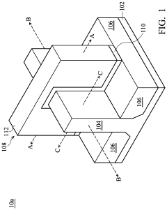
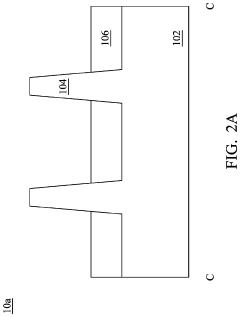
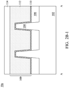
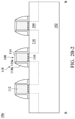
Method for forming fin field effect transistor device structure
PatentActiveUS20210313443A1
Innovation
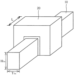
- A method involving sequential wet cleaning, plasma treatment, and additional wet cleaning of the source/drain recess to enlarge its width and improve surface quality, combined with growing an arc-shape source/drain epitaxial structure, enhances the distance control between the source/drain and gate structures.
Method of designing fin-based transistor for power optimization
PatentActiveTW201600988A
Innovation
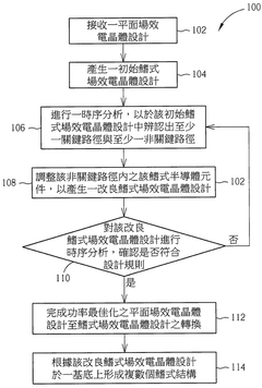
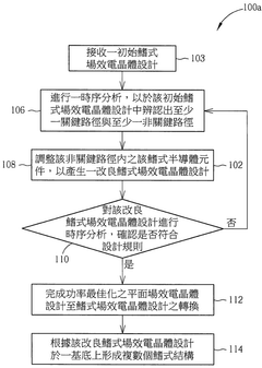
- A method is provided to design a fin structure transistor by identifying critical and non-critical paths in the initial FinFET design through timing analysis, and adjusting fin semiconductor elements in non-critical paths to reduce the number, width, or electrical connections of fins, thereby reducing power consumption.

Manufacturing Process Integration and Design for Manufacturability
The integration of FinFET technology into manufacturing processes represents a critical challenge in semiconductor fabrication. Successful implementation requires careful consideration of design-for-manufacturability (DFM) principles to maximize yield rates. Current manufacturing processes for FinFET devices involve complex multi-step lithography, etching, and deposition sequences that must be precisely controlled to achieve consistent fin dimensions and spacing. The three-dimensional nature of these structures introduces additional complexity compared to traditional planar transistors.
Process integration for FinFETs necessitates tight control over fin height, width, and pitch uniformity across the wafer. Advanced lithography techniques such as multi-patterning, extreme ultraviolet (EUV) lithography, and directed self-assembly (DSA) have been developed specifically to address these manufacturing challenges. Each approach offers different trade-offs between resolution capability, process complexity, and cost considerations that directly impact overall yield.
Design for manufacturability strategies for FinFETs focus on layout optimizations that accommodate process variations while maintaining electrical performance. Key DFM techniques include implementing redundant fins, optimizing gate-fin overlay tolerances, and incorporating dummy structures to improve pattern density uniformity. Statistical analysis of critical dimensions has become essential in predicting yield impacts and identifying design vulnerabilities before mass production begins.
The interface between design and manufacturing teams has evolved significantly with FinFET technology. Integrated design-manufacturing workflows now incorporate detailed process models that simulate the effects of manufacturing variations on device performance. These models enable designers to identify and mitigate yield-limiting factors early in the development cycle through techniques such as corner analysis and process-aware optimization.
Metrology and inspection capabilities have also advanced to support FinFET manufacturing. In-line monitoring systems now provide three-dimensional measurements of fin profiles, enabling real-time process adjustments to maintain yield targets. Feedback loops between inspection data and process controls have become increasingly sophisticated, allowing for adaptive manufacturing approaches that respond to detected variations.
Recent innovations in FinFET manufacturing integration include self-aligned multi-patterning techniques that reduce critical overlay requirements, atomic layer deposition methods for precise fin material control, and advanced etch chemistries that improve profile uniformity. These process enhancements, when combined with DFM-aware design practices, have demonstrated significant yield improvements in production environments, particularly for sub-10nm technology nodes.
Scaling Considerations for Sub-5nm FinFET Nodes
As semiconductor technology continues to advance beyond the 7nm node, scaling FinFET devices to sub-5nm dimensions presents significant challenges that directly impact manufacturing yield. The fundamental physics of semiconductor devices at these dimensions introduces quantum effects that cannot be ignored in design considerations. Electron tunneling becomes more pronounced, leading to increased leakage currents and power consumption challenges that must be addressed through innovative design approaches.
Material properties at sub-5nm scales exhibit greater variability, requiring more sophisticated process control mechanisms. Silicon channel dimensions approach atomic limits, necessitating consideration of alternative channel materials such as silicon-germanium alloys or III-V semiconductors that offer higher carrier mobility. These material transitions introduce new integration challenges that must be carefully managed to maintain yield metrics.
Gate control becomes increasingly difficult as dimensions shrink, requiring innovations in gate stack engineering. Multi-gate architectures beyond the traditional tri-gate FinFET design are being explored, including gate-all-around (GAA) structures that provide superior electrostatic control. The transition from FinFET to nanosheet or nanowire structures represents a critical evolutionary path for maintaining performance at sub-5nm nodes.
Lithography limitations present another scaling challenge, as even extreme ultraviolet (EUV) lithography approaches resolution limits at these dimensions. Multiple patterning techniques must be optimized to achieve the required feature sizes while minimizing edge placement errors and line edge roughness that can significantly impact device performance variability and yield.
Parasitic capacitance and resistance effects become increasingly dominant as dimensions shrink, requiring careful optimization of contact schemes and interconnect structures. Self-aligned contact processes must be refined to accommodate tighter pitch requirements while maintaining electrical isolation between adjacent structures.
Thermal management presents additional challenges as power density increases with scaling. Novel cooling solutions and thermally-aware design methodologies become essential to prevent performance degradation and reliability issues that would otherwise impact product yield. Thermal considerations must be integrated earlier in the design process rather than addressed as an afterthought.
Statistical variability in device parameters increases dramatically at sub-5nm nodes, necessitating robust design for manufacturing (DFM) methodologies that account for process variations. Advanced computational models that incorporate quantum effects and variability must be developed to accurately predict device behavior and optimize designs for maximum yield.
Unlock deeper insights with Patsnap Eureka Quick Research — get a full tech report to explore trends and direct your research. Try now!
Generate Your Research Report Instantly with AI Agent
Supercharge your innovation with Patsnap Eureka AI Agent Platform!