

Exploring OLED vs MicroLED in Advanced Manufacturing
OCT 24, 20259 MIN READ
Generate Your Research Report Instantly with AI Agent
PatSnap Eureka helps you evaluate technical feasibility & market potential.
Display Technology Evolution and Objectives
Display technology has undergone remarkable evolution since the introduction of cathode ray tubes (CRTs) in the early 20th century. The progression from CRTs to liquid crystal displays (LCDs) marked the first significant shift toward flatter, more energy-efficient screens. This transition was followed by the development of plasma display panels, which offered improved contrast ratios and viewing angles but struggled with power consumption issues. The early 2000s witnessed the emergence of organic light-emitting diode (OLED) technology, representing a paradigm shift in display capabilities with self-emissive pixels that eliminated the need for backlighting.
OLED technology has dominated premium display applications for over a decade, offering superior contrast ratios, wider viewing angles, and flexible form factors. However, challenges including burn-in issues, limited brightness, and manufacturing complexities have persisted. These limitations have created an opportunity for MicroLED technology, which promises to combine the best attributes of OLED with enhanced durability, brightness, and efficiency. First demonstrated in laboratories in the early 2010s, MicroLED represents the cutting edge of display innovation.
The current technological landscape is characterized by OLED's market maturity versus MicroLED's emerging potential. OLED manufacturing has achieved significant scale economies, with production yields improving and costs decreasing over time. Conversely, MicroLED remains in the early commercialization phase, with manufacturers working to overcome mass production challenges, particularly in the transfer and placement of millions of microscopic LED elements with near-perfect precision.
The primary objective of current research and development efforts is to determine the optimal technology pathway for next-generation displays across various applications. For consumer electronics, this means balancing visual performance with manufacturing scalability and cost-effectiveness. For automotive and industrial applications, considerations extend to durability under extreme conditions and operational longevity.
Technical goals include improving OLED manufacturing efficiency while extending panel lifespan and brightness capabilities. For MicroLED, objectives focus on developing reliable mass transfer techniques, reducing pixel pitch to enable higher resolution displays, and establishing cost-effective production methods that can compete with mature OLED manufacturing processes.
The convergence of these technologies with advanced manufacturing techniques represents a critical inflection point in display evolution. Industry projections suggest that while OLED will maintain dominance in the near term, MicroLED could potentially capture significant market share by the latter half of this decade, particularly in premium segments where performance advantages justify higher production costs. This technological transition will likely reshape supply chains and manufacturing infrastructure across the global electronics industry.
Market Analysis for Advanced Display Technologies
The display technology market is experiencing a significant shift as manufacturers increasingly focus on advanced solutions like OLED and MicroLED. The global display market reached approximately $148 billion in 2022 and is projected to grow at a CAGR of 7.5% through 2030, with premium display technologies driving much of this expansion.
OLED currently dominates the high-end display segment with roughly 30% market share in the overall display industry, but MicroLED is emerging as a formidable competitor in specific applications. Market segmentation reveals distinct adoption patterns: OLED maintains strong positioning in smartphones (65% of premium devices) and high-end televisions, while MicroLED is gaining traction in specialized sectors including automotive displays, premium large-format displays, and AR/VR applications.
Consumer electronics represents the largest application segment for both technologies, accounting for over 60% of advanced display implementation. However, industrial and automotive applications are growing at the fastest rates, with projected CAGRs exceeding 20% for MicroLED in these sectors through 2028.
Regional analysis indicates Asia-Pacific dominates manufacturing capacity, with South Korea and China leading OLED production (Samsung and LG Display controlling approximately 75% of global OLED panel production), while Taiwan is emerging as a significant hub for MicroLED development. North America and Europe remain important markets for consumption but contribute less to manufacturing output.
Price sensitivity analysis reveals a critical market dynamic: while OLED manufacturing costs have decreased by approximately 35% over the past five years due to economies of scale, MicroLED remains significantly more expensive to produce, with current costs estimated at 3-5 times higher than equivalent OLED panels. This cost differential represents the primary barrier to widespread MicroLED adoption.
Market forecasts suggest OLED will maintain dominance through mid-decade, but MicroLED is expected to capture increasing market share in premium segments starting around 2025-2026 as manufacturing processes mature and costs decline. The inflection point for broader MicroLED adoption is anticipated when production costs decrease to approximately 1.5 times that of OLED, expected around 2027-2028 based on current technology development trajectories.
Customer preference surveys indicate growing awareness of MicroLED benefits, with 72% of professional users and 45% of premium consumers expressing interest in MicroLED displays despite the higher price point, suggesting strong potential demand as the technology becomes more accessible.
OLED vs MicroLED: Technical Challenges
Both OLED and MicroLED technologies face significant technical challenges that impact their adoption in advanced manufacturing. OLED technology, despite its commercial maturity, continues to struggle with several persistent issues. Organic materials in OLEDs remain susceptible to degradation when exposed to oxygen and moisture, necessitating complex encapsulation solutions. This vulnerability contributes to shorter lifespans, particularly for blue OLED emitters which typically degrade faster than red and green counterparts, creating color balance issues over time.
Manufacturing scalability presents another major challenge for OLEDs. While small and medium-sized OLED panels have achieved production efficiency, large-format displays still face yield issues and cost barriers. The fine metal mask (FMM) process used for RGB OLED patterning becomes increasingly difficult to manage as display sizes increase, limiting resolution and manufacturing precision for larger panels.
MicroLED technology, though promising, faces even more formidable manufacturing hurdles. The mass transfer process—moving millions of tiny LED chips from growth substrates to display backplanes—remains the most significant technical bottleneck. Current approaches including pick-and-place, fluid assembly, and laser transfer methods all struggle with throughput, accuracy, and yield rates at commercial scales.
Defect management presents another critical challenge for MicroLED manufacturing. The technology's "all or nothing" pixel nature means that even minor defects can render entire pixels non-functional, unlike OLEDs where pixels might continue functioning at reduced efficiency. This creates stringent requirements for both initial manufacturing precision and repair processes.
Size uniformity and consistency across millions of MicroLED elements pose additional manufacturing difficulties. Variations in LED size, even at microscopic levels, can cause noticeable color and brightness inconsistencies across displays. Achieving uniform electrical and optical characteristics at mass production scales remains technically demanding.
Both technologies also face efficiency challenges. OLEDs struggle with power consumption, particularly for large-format and high-brightness applications. MicroLEDs offer theoretical efficiency advantages but currently face challenges in light extraction efficiency and electrical-to-optical conversion rates at micro-scale dimensions.
Cost factors compound these technical challenges. OLED manufacturing has benefited from years of investment but still faces high production costs for premium applications. MicroLED manufacturing requires entirely new production infrastructure and processes, with current costs prohibitively high for most consumer applications despite the technology's potential for eventual cost advantages through simplified structure and longer lifespans.
Current Manufacturing Solutions Comparison
01 OLED display structure and materials
Organic Light Emitting Diode (OLED) displays utilize organic compounds that emit light when electricity is applied. These displays feature multiple layers including cathode, organic layers, and anode. The organic materials can be designed to emit different colors, eliminating the need for backlighting. This technology offers advantages such as flexibility, thinness, energy efficiency, and superior contrast ratios compared to traditional LCD displays.- OLED display structure and materials: OLED displays utilize organic light-emitting materials that emit light when electricity is applied. These displays feature multiple layers including cathode, organic layers, and anode. The organic materials can be engineered for different colors and brightness levels. OLED technology offers advantages such as self-emission (no backlight needed), flexibility, and high contrast ratios. Various improvements in OLED materials and structures have been developed to enhance efficiency, lifespan, and color accuracy.
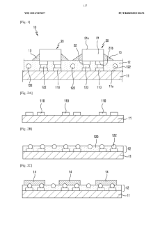
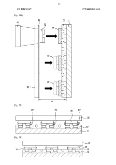
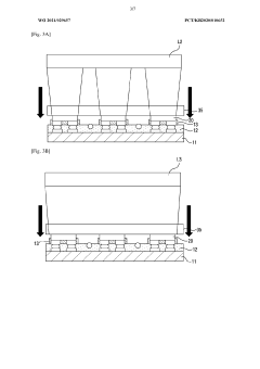
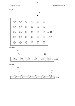
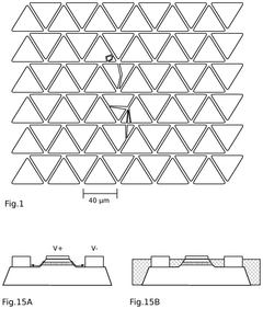
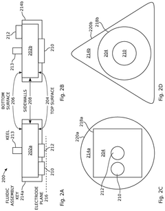
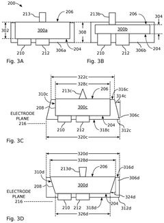
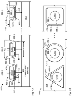
- MicroLED fabrication and integration: MicroLED technology involves the integration of microscopic LED arrays to create displays with exceptional brightness and efficiency. The fabrication process includes transfer techniques to position tiny LED elements onto display substrates. Various methods have been developed to improve yield rates and precision during the transfer process. MicroLED displays offer advantages including higher brightness, longer lifespan, and better energy efficiency compared to other display technologies.
- Display driving and control systems: Advanced driving and control systems are essential for both OLED and MicroLED displays. These systems include pixel addressing schemes, thin-film transistor (TFT) backplanes, and specialized integrated circuits. Various innovations focus on reducing power consumption while maintaining display performance. Compensation circuits are implemented to address issues like non-uniformity and aging effects in display panels. These control systems enable features such as variable refresh rates and adaptive brightness.
- Hybrid and flexible display technologies: Hybrid display technologies combine elements of OLED and MicroLED to leverage advantages of both. Flexible and foldable display implementations utilize specialized substrates and encapsulation techniques to enable bending without damage to the display elements. These technologies enable new form factors for devices including rollable, foldable, and stretchable displays. Special attention is given to the interface layers and connection points to maintain performance during repeated flexing or folding operations.
- Thermal management and reliability enhancements: Thermal management is critical for both OLED and MicroLED displays to ensure longevity and consistent performance. Various heat dissipation structures and materials have been developed to address thermal challenges. Reliability enhancements include protection against moisture and oxygen ingress, which can degrade organic materials in OLEDs. For MicroLEDs, specialized packaging techniques help maintain electrical connections and protect the microscopic elements. These improvements contribute to extended operational lifetimes and more stable performance characteristics over time.
02 MicroLED fabrication and integration
MicroLED technology involves the integration of microscopic LED arrays to create displays with high brightness and efficiency. The fabrication process includes transfer techniques to position tiny LED elements onto display substrates. These displays offer advantages such as higher brightness, longer lifespan, and better energy efficiency compared to other display technologies. The manufacturing challenges include precise alignment of microLEDs and establishing reliable electrical connections.Expand Specific Solutions03 Display driving and control systems
Advanced driving and control systems are essential for both OLED and MicroLED displays. These systems include thin-film transistor (TFT) backplanes, driver ICs, and control circuitry that manage pixel addressing, brightness control, and power management. Innovations in this area focus on reducing power consumption, improving refresh rates, and enabling features like local dimming for enhanced contrast and image quality.Expand Specific Solutions04 Display integration in devices and applications
OLED and MicroLED displays are being integrated into various devices including smartphones, televisions, wearables, and automotive displays. The integration involves considerations for form factor, power requirements, and environmental conditions. Flexible and foldable display implementations are particularly notable, allowing for innovative device designs. Applications extend to virtual reality, augmented reality, and transparent displays for next-generation user interfaces.Expand Specific Solutions05 Manufacturing processes and equipment
Specialized manufacturing processes and equipment are required for both OLED and MicroLED production. These include deposition systems for organic materials, transfer equipment for microLED placement, encapsulation technologies to protect sensitive components, and testing systems to ensure display quality. Innovations focus on improving yield rates, reducing production costs, and enabling mass production of these advanced display technologies.Expand Specific Solutions
Key Industry Players and Competitive Landscape
The OLED vs MicroLED display technology landscape is currently in a transitional phase, with OLED being mature and widely adopted while MicroLED remains in early commercialization stages. The global market for these advanced display technologies is projected to reach $200 billion by 2025, driven by demand for higher performance displays in consumer electronics and automotive applications. In terms of technical maturity, established players like Samsung Electronics, LG Electronics, and BOE Technology Group have achieved mass production capabilities for OLED, while MicroLED development is being pioneered by companies including Samsung, Apple, and specialized firms like Chengdu Vistar Optoelectronics. The competitive landscape features traditional display manufacturers expanding their portfolios alongside semiconductor companies like Applied Materials and Intel entering the space to capitalize on the convergence of display and semiconductor technologies.
BOE Technology Group Co., Ltd.
Technical Solution: BOE has developed comprehensive manufacturing solutions for both OLED and MicroLED technologies. For OLED production, BOE employs flexible AMOLED manufacturing with oxide TFT backplanes and inkjet printing deposition methods that reduce material waste by approximately 20% compared to traditional evaporation techniques. Their Gen 6 OLED production lines utilize low-temperature polysilicon (LTPS) technology for higher electron mobility. In the MicroLED space, BOE has pioneered a hybrid integration approach combining traditional LED manufacturing with advanced semiconductor processes. Their proprietary "micro-transfer printing" technology can handle LED chips as small as 30 micrometers with placement accuracy of ±1.5 micrometers. BOE has also developed a self-aligned structure that improves the aperture ratio of MicroLED displays by up to 60%, enhancing brightness while reducing power consumption.
Strengths: Vertically integrated supply chain; advanced inkjet printing capabilities for OLED; significant R&D investment in transfer technologies for MicroLED. Weaknesses: Lower yields in flexible OLED manufacturing compared to industry leaders; still developing mass production capabilities for commercial MicroLED displays; higher defect rates in early MicroLED prototypes.
Samsung Electronics Co., Ltd.
Technical Solution: Samsung has pioneered both OLED and MicroLED technologies with significant manufacturing innovations. For OLED, Samsung utilizes vacuum thermal evaporation (VTE) processes with fine metal masks (FMM) to deposit organic materials precisely. Their Quantum Dot (QD)-OLED technology combines quantum dots with blue OLED emitters to achieve superior color volume and viewing angles. In MicroLED manufacturing, Samsung employs a mass transfer process that can place millions of microscopic LEDs precisely onto substrates. Their "The Wall" MicroLED display uses chip-on-board technology with inorganic LED chips smaller than 100 micrometers. Samsung has also developed a proprietary surface mount technology for MicroLED that improves production yields by over 70% compared to earlier methods, enabling more efficient manufacturing at scale.
Strengths: Industry-leading production capacity for both technologies; proprietary mass transfer techniques for MicroLED; established supply chain integration. Weaknesses: High manufacturing costs for MicroLED displays; current size limitations for mass-market OLED panels; yield challenges in ultra-fine pitch MicroLED production.
Patent Analysis and Technical Innovations
Micro LED display and manufacturing method thereof
PatentWO2021029657A1
Innovation
- The use of an anisotropic conductive film with conductive particles for electrically and physically connecting micro LED chips to a substrate, involving bonding, laser transfer, and heating to form a conductive structure between the chip's connection pad and the substrate's circuit part.
Encapsulated light emitting diodes for selective fluidic assembly
PatentActiveUS12119432B2
Innovation
- The use of partially encapsulated semiconductor-based inorganic micro-LEDs with a patternable polymer encapsulant that protects the LEDs from collisions and optimizes their shape for efficient assembly, allowing for higher speed and yield while preventing defects, and enabling precise alignment of LED colors on a display substrate.
Supply Chain Considerations
The supply chain dynamics for OLED and MicroLED technologies present distinct challenges and opportunities that significantly impact manufacturing strategies and market adoption. OLED supply chains have matured considerably over the past decade, with established production ecosystems primarily concentrated in East Asia. South Korean manufacturers like Samsung and LG Display dominate high-end OLED panel production, while Chinese companies have rapidly expanded capacity for mid-range applications. This geographic concentration creates potential vulnerabilities to regional disruptions, as evidenced during recent global supply chain crises.
MicroLED supply chains, by contrast, remain nascent and fragmented. The technology requires specialized materials and components from diverse suppliers, including rare earth phosphors, semiconductor substrates, and precision assembly equipment. This complexity introduces multiple potential bottlenecks, particularly in the mass transfer process where millions of microscopic LED chips must be precisely positioned. Current manufacturing approaches rely heavily on specialized equipment providers, creating dependencies that may constrain production scaling.
Raw material considerations further differentiate these technologies. OLED production depends on organic compounds and flexible substrates that have established supply networks but face periodic shortages during demand surges. MicroLED requires semiconductor-grade materials with higher purity standards and specialized rare earth elements, potentially exposing manufacturers to geopolitical supply risks and price volatility.
Inventory management presents another critical distinction. OLED panels have relatively standardized production processes allowing for more predictable lead times and inventory planning. MicroLED manufacturing currently involves longer production cycles with higher variability, necessitating more sophisticated inventory strategies and potentially higher working capital requirements.
Sustainability considerations are increasingly influencing supply chain decisions. OLED manufacturing processes generate hazardous waste from organic solvents and require energy-intensive vacuum deposition. MicroLED production generally has lower chemical waste profiles but may face scrutiny regarding rare earth material sourcing and energy consumption during precision manufacturing steps.
As advanced manufacturing facilities contemplate technology adoption, supply chain resilience has become a paramount consideration. Diversification strategies, including geographic distribution of suppliers and vertical integration of critical components, are being implemented particularly for MicroLED development. Companies are also investing in alternative materials research to mitigate potential supply constraints, with synthetic alternatives to rare earth phosphors showing promising results in laboratory settings.
Environmental Impact and Sustainability
The environmental impact of display technologies has become increasingly important as manufacturers and consumers alike prioritize sustainability. When comparing OLED and MicroLED technologies, several critical environmental factors must be considered throughout their lifecycle, from production to disposal.
OLED manufacturing processes generally consume less energy than traditional LCD production, but still involve potentially harmful chemicals and rare materials. The organic compounds in OLEDs require fewer toxic substances compared to older technologies, yet the production still generates waste that requires careful management. Additionally, the encapsulation materials used to protect OLEDs from moisture and oxygen degradation often include non-biodegradable components.
MicroLED manufacturing, while promising in many aspects, currently faces sustainability challenges due to its complex production processes. The fabrication of microscopic LED arrays demands precision equipment that consumes significant energy. However, MicroLEDs contain fewer toxic materials than OLEDs and don't require the same organic compounds that can be environmentally problematic. The inorganic nature of MicroLEDs potentially makes them more recyclable at end-of-life.
Energy efficiency during operation represents a significant environmental advantage for both technologies. OLEDs consume less power than traditional displays because they don't require backlighting, especially when displaying darker content. MicroLEDs potentially offer even greater energy efficiency, with some estimates suggesting 30% less power consumption than OLEDs, which could substantially reduce carbon footprints over product lifespans.
Longevity also factors into environmental impact calculations. MicroLEDs demonstrate superior resistance to burn-in and degradation compared to OLEDs, potentially extending useful life by several years. This durability translates to fewer replacement cycles and reduced electronic waste generation over time.
End-of-life considerations reveal further distinctions. OLED displays present recycling challenges due to their organic components and multi-layer construction. MicroLED displays, while also complex, contain more recoverable inorganic materials that may be more amenable to existing recycling infrastructure. However, both technologies require specialized recycling processes that are still evolving.
Water usage in manufacturing represents another environmental concern. OLED production typically requires significant quantities of ultra-pure water for cleaning processes, while MicroLED manufacturing may require less water but more energy-intensive precision fabrication steps. As water scarcity becomes more prevalent globally, this factor gains importance in sustainability assessments.
Unlock deeper insights with PatSnap Eureka Quick Research — get a full tech report to explore trends and direct your research. Try now!
Generate Your Research Report Instantly with AI Agent
Supercharge your innovation with PatSnap Eureka AI Agent Platform!