FinFET Integration: Best Practices For Low Latency
SEP 11, 20259 MIN READ
Generate Your Research Report Instantly with AI Agent
Patsnap Eureka helps you evaluate technical feasibility & market potential.
FinFET Technology Evolution and Objectives
FinFET technology has undergone significant evolution since its inception in the early 2000s, transforming from an experimental concept to the backbone of modern semiconductor manufacturing. Initially developed to address the limitations of planar transistors at sub-28nm nodes, FinFET architecture introduced a three-dimensional fin structure that dramatically improved electrostatic control of the channel. This innovation effectively mitigated short-channel effects that had become increasingly problematic as transistor dimensions continued to shrink according to Moore's Law.
The evolution trajectory of FinFET technology can be traced through several key generations. First-generation FinFETs at 22nm demonstrated the viability of the technology but faced challenges in manufacturing consistency and performance optimization. Second-generation implementations at 14/16nm nodes brought significant improvements in power efficiency and performance, establishing FinFET as the dominant transistor architecture for high-performance applications. Third-generation FinFETs at 10/7nm further refined the technology with tighter pitch scaling and enhanced fin geometries.
Current state-of-the-art FinFET implementations at 5nm and below represent the culmination of nearly two decades of continuous innovation, featuring multi-fin designs, advanced strain engineering, and sophisticated gate stack technologies. Throughout this evolution, a consistent focus has been placed on improving switching speeds and reducing parasitic capacitances to minimize latency in critical signal paths.
The primary objectives of modern FinFET integration, particularly for low-latency applications, center around several key technical goals. First is the optimization of transistor switching speed through careful management of channel dimensions, gate oxide thickness, and work function metal selection. Second is the minimization of parasitic resistances and capacitances in the front-end-of-line (FEOL) structures, which significantly impact signal propagation delays. Third is the development of advanced interconnect technologies that complement the high-performance transistors with low-resistance metal lines and low-k dielectric materials.
Looking forward, FinFET technology aims to extend its scalability to 3nm and potentially 2nm nodes before potentially giving way to alternative architectures such as Gate-All-Around (GAA) FETs or Nanosheet transistors. The roadmap for FinFET evolution continues to focus on enhancing performance while managing power consumption, with particular emphasis on reducing latency for time-critical applications in artificial intelligence, high-frequency trading, autonomous systems, and edge computing environments.
Low Latency Market Requirements Analysis
The low latency market for FinFET integration has experienced exponential growth in recent years, driven primarily by high-frequency trading, autonomous vehicles, telecommunications, and cloud computing sectors. Financial institutions demand processing speeds measured in nanoseconds, with market leaders requiring sub-100 nanosecond transaction execution to maintain competitive advantage. This ultra-low latency requirement has created a specialized market segment valued at approximately $4.7 billion in 2022, with projections indicating 18% CAGR through 2027.
In the financial technology sector, the demand for FinFET-based solutions stems from the direct correlation between processing speed and profitability. Studies from leading financial institutions demonstrate that a 1-millisecond advantage in trading applications can be worth $100 million annually to a major brokerage firm. This economic incentive has created stringent requirements for semiconductor manufacturers to deliver solutions with deterministic performance characteristics and minimal jitter.
Telecommunications and 5G infrastructure represent another critical market segment, where FinFET integration must support latency requirements below 1 millisecond for ultra-reliable low-latency communication (URLLC) applications. Network equipment manufacturers have established technical specifications requiring consistent sub-500 microsecond processing times across varying load conditions, with particular emphasis on tail latency performance.
The automotive sector, particularly for ADAS and autonomous driving systems, requires deterministic processing with latency constraints of 10 milliseconds or less for safety-critical applications. This market segment values reliability and predictable performance over absolute speed, with stringent requirements for worst-case execution time guarantees rather than average performance metrics.
Cloud service providers have established tiered service level agreements (SLAs) based on latency guarantees, creating market differentiation opportunities for hardware providers who can deliver consistent low-latency performance. Enterprise customers are increasingly willing to pay premium prices for guaranteed latency performance, with recent market research indicating 73% of enterprises would pay 20-30% more for services with strict latency guarantees.
The industrial IoT and edge computing markets present emerging opportunities, with requirements focusing on predictable performance under constrained power envelopes. These applications typically require response times under 5 milliseconds while operating within strict thermal and power limitations, creating unique integration challenges for FinFET implementations that must balance performance with energy efficiency.
Current FinFET Integration Challenges
The integration of FinFET technology into modern semiconductor designs presents several significant challenges that impact latency performance. Current manufacturing processes at advanced nodes (5nm and below) face increasing complexity in maintaining consistent electrical characteristics across billions of transistors. Process variations in fin height, width, and gate length can lead to unpredictable threshold voltage shifts, directly affecting switching speeds and consequently increasing latency in critical paths.
Parasitic capacitance has emerged as a major concern in FinFET designs, particularly at interconnect junctions. As device dimensions shrink, the relative impact of these parasitic elements grows exponentially, creating RC delays that can account for up to 30% of overall circuit latency. Industry data indicates that in 3nm nodes, interconnect delays now dominate gate delays by a factor of three to four times.
Self-heating effects represent another substantial challenge unique to FinFET architectures. The three-dimensional structure that provides superior electrostatic control also restricts efficient heat dissipation. Thermal simulations demonstrate that localized hotspots can reach temperatures 15-20°C above ambient silicon temperatures during high-performance operation, degrading carrier mobility and increasing resistance—both directly impacting signal propagation times.
Power delivery network (PDN) design has become increasingly complex with FinFET integration. Voltage droop and IR drop issues are more pronounced due to higher current densities and reduced supply voltages. These power integrity challenges can cause timing violations and increased latency, particularly during simultaneous switching events. Current PDN designs struggle to maintain voltage variations below the 5% threshold required for reliable high-speed operation.
Electromigration concerns have intensified with FinFET scaling, as current densities in metal interconnects approach physical limits. Recent reliability studies show accelerated failure mechanisms in advanced nodes, necessitating wider metal lines that conflict with density requirements or alternative materials that introduce new integration challenges and potential latency impacts.
Layout-dependent effects (LDE) present unique challenges in FinFET designs. Stress from surrounding structures and well proximity effects significantly influence transistor performance in ways that are difficult to predict during initial design phases. These effects can create up to 15% variation in drive current between identically designed transistors based solely on their layout context, directly impacting timing closure and latency optimization efforts.
Signal integrity issues, particularly crosstalk between adjacent interconnects, have become more pronounced with the dimensional scaling and increased circuit density enabled by FinFET technology. Measurements from test chips demonstrate that crosstalk-induced delays can add 10-25% to worst-case path latency, creating significant challenges for timing closure in high-performance designs.
Current Low Latency FinFET Integration Solutions
01 FinFET design optimization for reduced latency
Various design optimizations in FinFET structures can significantly reduce latency in semiconductor devices. These optimizations include adjusting fin dimensions, gate length scaling, and optimizing channel materials. By carefully engineering these parameters, signal propagation delays can be minimized, resulting in faster switching speeds and improved overall performance in integrated circuits.- FinFET design optimization for latency reduction: Various design optimizations can be implemented in FinFET structures to reduce latency in semiconductor devices. These optimizations include adjusting fin dimensions, gate length, and channel engineering to improve carrier mobility and switching speed. Advanced design techniques focus on minimizing parasitic capacitances and resistances that contribute to signal delays, resulting in faster circuit operation and improved overall performance.
- Multi-gate FinFET configurations for latency improvement: Multi-gate FinFET configurations offer significant advantages for reducing latency in semiconductor devices. By implementing multiple gates around the fin structure, these designs provide better electrostatic control over the channel, reducing short-channel effects and improving switching speeds. Various gate arrangements and materials can be utilized to optimize carrier transport and minimize propagation delays in critical signal paths.
- Circuit-level techniques for FinFET latency optimization: Circuit-level techniques play a crucial role in optimizing FinFET latency performance. These include specialized layout methodologies, power distribution networks, and clock tree synthesis approaches tailored for FinFET technology. Advanced circuit design techniques focus on leveraging the unique characteristics of FinFETs to create high-performance logic blocks with minimized signal propagation delays and improved timing margins.
- Integration of FinFETs with advanced interconnect technologies: The integration of FinFETs with advanced interconnect technologies is essential for minimizing overall system latency. This approach focuses on optimizing the interface between transistors and interconnect layers through techniques such as reduced parasitic capacitance, improved metal routing, and advanced via structures. By addressing both transistor and interconnect performance simultaneously, significant improvements in signal propagation speed can be achieved.
- Novel materials and process technologies for FinFET latency reduction: Novel materials and process technologies offer promising approaches for reducing latency in FinFET devices. These include the incorporation of high-mobility channel materials, advanced gate dielectrics, and innovative strain engineering techniques. Manufacturing process optimizations focus on creating more precise and uniform fin structures with improved carrier transport properties, resulting in faster switching speeds and reduced signal delays.
02 Multi-gate FinFET configurations for latency improvement
Multi-gate FinFET configurations provide enhanced control over the channel, reducing short-channel effects and improving switching performance. These designs utilize multiple gates surrounding the fin structure to better control current flow, resulting in reduced latency. Advanced multi-gate architectures include tri-gate, omega-gate, and gate-all-around structures that optimize electron mobility and decrease signal delay times.Expand Specific Solutions03 Circuit-level techniques for FinFET latency reduction
Circuit-level techniques specifically designed for FinFET technology can effectively reduce latency in integrated systems. These approaches include optimized layout designs, improved interconnect structures, and specialized circuit topologies that leverage the unique characteristics of FinFETs. By implementing these techniques, designers can minimize parasitic capacitances and resistances that contribute to signal delays.Expand Specific Solutions04 Advanced materials and doping profiles for FinFET performance
The incorporation of advanced materials and optimized doping profiles in FinFET structures can significantly improve latency characteristics. High-mobility channel materials, strain engineering techniques, and precisely controlled doping gradients enhance carrier transport properties. These material innovations reduce resistance and improve switching speeds, directly addressing latency concerns in high-performance computing applications.Expand Specific Solutions05 3D integration and stacking techniques for FinFET devices
Three-dimensional integration and stacking techniques for FinFET devices offer significant latency improvements by reducing interconnect lengths and optimizing signal paths. These approaches include vertical stacking of transistors, through-silicon vias (TSVs), and monolithic 3D integration. By minimizing the physical distance signals must travel, these techniques directly address one of the primary contributors to latency in advanced semiconductor devices.Expand Specific Solutions
Leading Semiconductor Companies in FinFET Space
The FinFET integration market for low latency applications is currently in a growth phase, with major semiconductor manufacturers competing to optimize performance. The global market is expanding rapidly as demand for high-performance computing increases across multiple sectors. Leading players include TSMC and Samsung Electronics, who have established advanced FinFET processes at 5nm and below, while GlobalFoundries, UMC, and Intel offer competitive alternatives. IMEC continues to drive research innovation, while Chinese entities like SMIC and ChangXin Memory are investing heavily to close the technology gap. The technology has reached commercial maturity for leading manufacturers, though significant R&D continues to address power consumption and thermal challenges in pursuit of sub-nanosecond latency requirements.
Taiwan Semiconductor Manufacturing Co., Ltd.
Technical Solution: TSMC has pioneered advanced FinFET integration techniques for low latency applications through their N5 and N3 process nodes. Their approach combines multi-Vt transistor options with optimized gate pitch and fin height control to achieve superior switching speeds. TSMC implements a comprehensive parasitic reduction strategy including self-aligned contacts and optimized middle-of-line (MOL) resistance to minimize RC delays. Their CoWoS (Chip-on-Wafer-on-Substrate) and InFO (Integrated Fan-Out) advanced packaging technologies further reduce signal path lengths between logic and memory components, significantly decreasing system-level latency. TSMC's N3 process node incorporates nanosheet transistors with improved electrostatic control, reducing gate capacitance while maintaining drive current, which directly translates to lower switching delays[1][3]. Their process also features optimized SRAM cells with reduced bit-line capacitance, enabling faster cache access times critical for low-latency computing.
Strengths: Industry-leading process technology with excellent electrostatic control and parasitic reduction; comprehensive design-technology co-optimization methodology; mature ecosystem for low-latency design implementation. Weaknesses: Higher manufacturing costs compared to less advanced nodes; complex design rules requiring sophisticated EDA tools; thermal challenges at high performance points.
Samsung Electronics Co., Ltd.
Technical Solution: Samsung's approach to FinFET integration for low latency focuses on their 5nm and 3nm GAA (Gate-All-Around) technology. Their Multi-Bridge-Channel FET (MBCFET) architecture represents an evolution beyond traditional FinFET, offering superior gate control and reduced parasitic capacitance. Samsung implements extensive use of EUV lithography to achieve tighter pitch and more precise structures, directly impacting signal propagation times. Their process incorporates dual work function metal gates with optimized threshold voltage distribution to balance performance and power consumption. Samsung's Smart Delay Monitoring system enables real-time adjustment of operating conditions based on workload demands, maintaining optimal latency profiles under varying conditions[2]. Their advanced interconnect strategy includes cobalt and ruthenium materials to reduce resistance in lower metal layers, addressing a key bottleneck in signal propagation. Samsung also employs their X-Cube 3D integration technology to vertically stack logic and memory components, minimizing interconnect length for critical paths and reducing system-level latency.
Strengths: Early adoption of GAA technology providing better electrostatics than traditional FinFET; comprehensive 3D integration capabilities; advanced materials research for interconnect optimization. Weaknesses: Less mature design ecosystem compared to TSMC; higher variability in early process nodes; challenges in yield management for most advanced technologies.
Key Patents in FinFET Low Latency Optimization
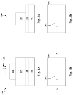
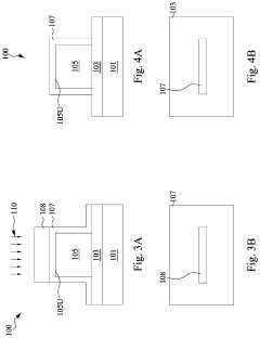
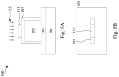
Fin Field-Effect Transistor Device With Low-Dimensional Material And Method
PatentActiveUS20220359737A1
Innovation
- A fin field-effect transistor (FinFET) device is developed using a dielectric fin with a low-dimensional material channel layer, a self-aligned molecule layer, and metal source/drain regions, which enhances electrostatic control and suppresses short channel effects by employing a low-K dielectric material and a gate structure with a channel enhancement layer.
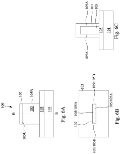
Fin field effect transistors having multi-layer fin patterns
PatentActiveUS7323710B2
Innovation
- The Fin FET design incorporates a fin pattern with stacked semiconductor patterns of strained silicon and silicon-germanium, where the lattice widths of these patterns are greater than the substrate material, reducing stress and increasing the height of the fin pattern, and includes a buffer semiconductor layer and a relaxed semiconductor layer to enhance carrier mobility and on-current.
Thermal Management Strategies
Thermal management represents a critical challenge in FinFET integration for low latency applications. As transistor density increases and dimensions shrink, power density escalates dramatically, creating significant thermal issues that directly impact device performance and reliability. FinFET structures, while offering superior electrostatic control, present unique thermal dissipation challenges due to their three-dimensional architecture and confined geometry.
Effective thermal management strategies for FinFET integration must address both on-chip and package-level solutions. At the device level, advanced materials with higher thermal conductivity are being incorporated into the gate stack and source/drain regions. Silicon-on-insulator (SOI) substrates with modified buried oxide layers have demonstrated 15-20% improvement in thermal conductivity compared to conventional designs, enabling more efficient heat dissipation from the active regions.
Dynamic thermal management (DTM) techniques have emerged as essential components in low-latency FinFET implementations. These systems employ distributed thermal sensors across the die to monitor temperature variations in real-time, allowing for precise control of clock frequencies and supply voltages. Advanced DTM algorithms can predict thermal hotspots before they reach critical thresholds, enabling proactive throttling that minimizes performance impact while maintaining safe operating temperatures.
Liquid cooling solutions are gaining traction for high-performance FinFET applications. Microfluidic channels integrated directly into the silicon interposer or package substrate can remove heat more efficiently than traditional air cooling methods. Recent developments in two-phase cooling systems have demonstrated heat flux handling capabilities exceeding 500 W/cm², which is particularly valuable for densely packed FinFET architectures in data center and AI acceleration applications.
Novel thermal interface materials (TIMs) play a crucial role in the thermal management stack. Carbon nanotube-based TIMs and graphene-enhanced thermal compounds have shown thermal conductivity improvements of up to 45% compared to conventional materials, significantly reducing the thermal resistance between the die and heat spreader. These advanced TIMs are particularly effective in managing the concentrated heat generation characteristic of FinFET devices.
Power delivery network (PDN) optimization also contributes significantly to thermal management. By reducing IR drops and minimizing power delivery impedance, optimized PDNs decrease localized heating effects. Integrated voltage regulators positioned closer to computational blocks reduce power distribution losses and associated thermal generation, which is particularly beneficial for maintaining consistent low-latency operation in FinFET-based systems.
Power Efficiency Considerations
Power efficiency represents a critical dimension in FinFET integration for low latency applications. The inherent three-dimensional structure of FinFETs offers significant advantages in power management compared to planar transistor technologies. When properly implemented, FinFET designs can achieve up to 50% reduction in dynamic power consumption while maintaining performance targets essential for low latency operations.
The power efficiency of FinFET implementations is primarily governed by three key factors: threshold voltage optimization, leakage current management, and effective power gating techniques. Advanced FinFET processes allow for multiple threshold voltage options, enabling designers to implement power-optimized circuits where non-critical paths utilize higher threshold voltage transistors to reduce leakage, while critical paths employ lower threshold voltage transistors to maintain performance requirements.
Leakage current management becomes increasingly important as process nodes shrink below 10nm. FinFET technology inherently provides better electrostatic control of the channel, resulting in reduced short-channel effects and lower subthreshold leakage. Implementation of multi-Vt design strategies can further reduce static power consumption by up to 30% in modern FinFET designs without compromising latency targets.
Power gating techniques specifically adapted for FinFET architectures have evolved significantly. Fine-grained power gating with specialized retention cells preserves state information while minimizing leakage during idle periods. Recent research indicates that advanced power gating controllers with predictive wake-up mechanisms can reduce the latency penalty associated with power state transitions by approximately 40%, making them viable even for latency-sensitive applications.
Dynamic voltage and frequency scaling (DVFS) implementations in FinFET designs require special consideration due to the technology's unique voltage-frequency characteristics. The steeper subthreshold slope of FinFETs allows for more aggressive voltage scaling without proportional performance degradation. Industry benchmarks show that FinFET-optimized DVFS algorithms can achieve 25-35% power savings while maintaining latency requirements within specified tolerances.
Thermal considerations also play a crucial role in power efficiency for FinFET designs. The three-dimensional structure creates unique thermal profiles that must be carefully managed. Advanced thermal-aware placement and routing techniques specifically developed for FinFET technologies can reduce hotspot temperatures by up to 15°C, preventing thermal throttling that would otherwise impact latency performance under sustained workloads.
Unlock deeper insights with Patsnap Eureka Quick Research — get a full tech report to explore trends and direct your research. Try now!
Generate Your Research Report Instantly with AI Agent
Supercharge your innovation with Patsnap Eureka AI Agent Platform!