

FinFET Patterning Techniques: Scale And Resolution
SEP 11, 20259 MIN READ
Generate Your Research Report Instantly with AI Agent
PatSnap Eureka helps you evaluate technical feasibility & market potential.
FinFET Evolution and Scaling Objectives
FinFET technology emerged as a revolutionary advancement in semiconductor manufacturing, evolving from traditional planar transistors to address the increasing challenges of device scaling. The journey began in the early 2000s when researchers at the University of California, Berkeley first demonstrated the concept of a three-dimensional transistor structure. This innovation marked a significant departure from conventional MOSFET designs, introducing a fin-shaped channel that extends vertically from the substrate surface.
The evolution of FinFET technology has been driven primarily by the semiconductor industry's relentless pursuit of Moore's Law, which predicts the doubling of transistor density approximately every two years. As planar transistors approached their physical scaling limits around the 22nm node, FinFETs emerged as the solution to continue miniaturization while maintaining performance improvements and power efficiency.
Intel's introduction of Tri-Gate transistors (their implementation of FinFET) at the 22nm node in 2011 represented the first commercial deployment of this technology. This milestone demonstrated that FinFETs could deliver approximately 37% performance improvement at low voltage compared to planar transistors, while consuming less than half the power at the same performance level.
The scaling objectives for FinFET technology are multifaceted, focusing on dimensional reduction, performance enhancement, and power optimization. Key metrics include reducing fin width and pitch to increase transistor density, minimizing gate length to improve switching speed, and optimizing fin height to balance performance with manufacturability constraints. The industry has successfully scaled FinFETs from initial 22nm implementations down to current 5nm processes, with research targeting 3nm and beyond.
Critical to achieving these scaling objectives has been the development of advanced patterning techniques. As dimensions shrink below the wavelength of light used in lithography systems, innovative approaches such as multi-patterning, extreme ultraviolet lithography (EUV), and directed self-assembly have become essential to define the intricate fin structures with the required precision.
The technical goals for future FinFET scaling include achieving sub-5nm gate lengths, fin widths below 5nm, and pitches approaching 20nm or less. These ambitious targets necessitate overcoming significant challenges in lithography resolution, pattern fidelity, and process variability control. Additionally, as dimensions continue to shrink, quantum effects and variability become increasingly prominent, requiring novel materials and process innovations to maintain device performance and reliability.
Looking forward, the semiconductor industry is exploring evolutionary improvements to the FinFET architecture, such as nanosheet or gate-all-around transistors, which represent the logical progression of the multi-gate concept pioneered by FinFETs. These next-generation structures aim to extend the benefits of three-dimensional transistor designs to even smaller technology nodes, ensuring continued advancement along the historical scaling trajectory.
Market Drivers for Advanced Semiconductor Nodes
The semiconductor industry's relentless pursuit of performance improvements and power efficiency continues to drive the development of advanced process nodes. The transition from planar transistors to FinFET architecture marked a pivotal moment in semiconductor manufacturing, enabling continued scaling beyond what was previously thought possible with traditional technologies. This evolution is primarily driven by several key market factors that collectively shape the demand for increasingly sophisticated patterning techniques.
Consumer electronics, particularly smartphones and tablets, represent the most significant market driver for advanced nodes. These devices require processors that deliver higher performance while consuming less power, all within increasingly compact form factors. The competitive smartphone market has established a predictable upgrade cycle that demands annual improvements in processing capabilities, creating consistent pressure for semiconductor manufacturers to advance their process technologies.
Data centers and cloud computing infrastructure constitute another crucial market segment pushing the boundaries of semiconductor technology. The exponential growth in data processing requirements, accelerated by artificial intelligence and machine learning applications, necessitates chips with greater transistor density and improved energy efficiency. These applications often operate in power-constrained environments where the performance-per-watt metric is paramount.
Automotive electronics have emerged as a rapidly growing market driver for advanced semiconductor nodes. The increasing integration of advanced driver-assistance systems (ADAS), autonomous driving capabilities, and in-vehicle infotainment systems requires sophisticated processing power that can operate reliably in challenging environmental conditions. This sector's stringent requirements for reliability and longevity create unique challenges for semiconductor manufacturing processes.
The Internet of Things (IoT) ecosystem presents contradictory demands that nonetheless influence advanced node development. While many IoT devices prioritize cost-effectiveness over cutting-edge performance, the aggregation and processing of IoT-generated data require high-performance computing capabilities that benefit from advanced process technologies.
High-performance computing applications, including scientific research, financial modeling, and weather forecasting, continue to push the limits of computational capabilities. These applications demand the absolute maximum in processing power, making them natural consumers of chips manufactured using the most advanced nodes available.
The economics of semiconductor manufacturing also play a crucial role in driving advanced node development. While the cost per transistor historically decreased with each new node, recent generations have seen diminishing returns on this front. Nevertheless, the overall system-level benefits and performance improvements continue to justify the investment in advanced process technologies for high-value applications.
Current FinFET Patterning Challenges
As FinFET technology continues to scale below 10nm nodes, the semiconductor industry faces increasingly complex patterning challenges. The fundamental issue stems from the physical limitations of traditional lithography techniques when attempting to create the three-dimensional fin structures that define FinFET architecture. Current optical lithography systems, even with advanced immersion techniques, struggle to achieve the resolution required for sub-10nm features without significant process complications.
The primary challenge lies in the resolution-pitch trade-off. As device dimensions shrink, the ability to pattern closely spaced fins with high fidelity becomes exponentially more difficult. Current 193nm immersion lithography reaches its theoretical resolution limit around 40nm pitch, yet modern FinFET designs require pitches approaching 20nm or less. This fundamental gap necessitates complex multi-patterning schemes that increase process steps, manufacturing costs, and potential defect sources.
Edge placement error (EPE) represents another critical challenge in current FinFET patterning. As dimensions shrink, even nanometer-scale misalignments between different patterning layers can significantly impact device performance. Industry data indicates that EPE control must be maintained within 1-2nm for advanced nodes, pushing metrology and process control systems to their limits. This precision requirement cascades through the entire manufacturing process, affecting yield and reliability.
Line edge roughness (LER) and line width roughness (LWR) have emerged as major concerns that directly impact device variability. At sub-10nm dimensions, atomic-scale variations in fin edges translate to significant performance variations across a chip. Current patterning techniques struggle to achieve the sub-1nm LER control required for consistent device performance, creating yield and reliability challenges that compound at the wafer scale.
Material limitations further complicate the patterning landscape. Resist materials must simultaneously provide high resolution, low LER, sufficient etch resistance, and pattern fidelity—a combination that becomes increasingly difficult to achieve at smaller dimensions. Current resist systems often require trade-offs between these properties, forcing complex process optimizations that vary by manufacturer and technology node.
Integration challenges between patterning steps represent another significant hurdle. Modern FinFET fabrication requires precise coordination between multiple lithography, deposition, and etch steps. Any misalignment or process variation compounds through the manufacturing sequence, potentially resulting in non-functional devices. The industry currently relies on sophisticated process control systems and design-technology co-optimization to manage these integration challenges, but fundamental physical limitations remain.
State-of-the-Art FinFET Patterning Solutions
01 Advanced lithography techniques for FinFET patterning
Advanced lithography techniques are essential for achieving the high resolution required in FinFET fabrication. These techniques include extreme ultraviolet (EUV) lithography, multiple patterning, and optical proximity correction, which enable the creation of nanoscale features with precise dimensions and spacing. These methods help overcome the resolution limitations of traditional lithography and allow for scaling of FinFET devices to smaller nodes while maintaining pattern fidelity.- Advanced lithography techniques for FinFET patterning: Advanced lithography techniques are essential for achieving the high resolution required in FinFET fabrication. These techniques include extreme ultraviolet (EUV) lithography, multiple patterning, and directed self-assembly. These methods enable the creation of smaller feature sizes and tighter pitches necessary for modern FinFET structures, overcoming the resolution limitations of traditional lithography approaches while maintaining pattern fidelity at nanometer scales.
- Multi-patterning and spacer-based techniques: Multi-patterning and spacer-based techniques are widely used to overcome resolution limitations in FinFET fabrication. These approaches involve multiple lithography and etching steps to create patterns beyond what a single exposure can achieve. Self-aligned double patterning (SADP) and self-aligned quadruple patterning (SAQP) are particularly valuable for creating high-density fin structures with precise dimensions and spacing, enabling scaling to smaller technology nodes.
- Computational and design techniques for pattern optimization: Computational and design techniques play a crucial role in optimizing FinFET patterning. These include optical proximity correction (OPC), design rule checking (DRC), and layout optimization algorithms that compensate for lithographic distortions. Advanced modeling and simulation tools help predict and mitigate patterning issues before fabrication, ensuring that the final structures meet the required specifications for performance and reliability at increasingly smaller scales.
- Novel materials and etching processes for fin formation: Novel materials and specialized etching processes are being developed to improve FinFET patterning resolution and quality. These include advanced hard mask materials, selective deposition techniques, and highly anisotropic etching processes that enable precise fin formation. Atomic layer deposition and atomic layer etching provide atomic-level control over dimensions, while specialized etch chemistries help achieve vertical fin profiles with minimal damage, critical for maintaining electrical performance as devices scale down.
- Integration schemes for high-density FinFET structures: Advanced integration schemes are essential for creating high-density FinFET structures with optimal electrical characteristics. These include self-aligned gate processes, cut mask techniques for fin segmentation, and methods for controlling fin height and width uniformity across the wafer. Novel approaches for source/drain formation and contact integration help maintain performance while scaling, addressing challenges such as parasitic resistance and capacitance that become increasingly significant at smaller dimensions.
02 Self-aligned double/multiple patterning for FinFET structures
Self-aligned double patterning (SADP) and multiple patterning techniques are widely used for FinFET fabrication to achieve sub-lithographic feature sizes. These approaches involve creating spacers on the sidewalls of sacrificial patterns and subsequently removing the original pattern, effectively doubling the pattern density. This technique enables the formation of closely spaced, high-aspect-ratio fin structures that are critical for high-performance FinFET devices while overcoming optical lithography limitations.Expand Specific Solutions03 Computational lithography and design optimization for FinFET scaling
Computational lithography and design optimization techniques play a crucial role in FinFET patterning. These include model-based optical proximity correction (OPC), source mask optimization (SMO), and inverse lithography technology (ILT). Advanced simulation tools help predict and correct for pattern distortions, enabling more accurate transfer of designed patterns to silicon. These computational approaches are essential for achieving the resolution and pattern fidelity required for advanced FinFET nodes.Expand Specific Solutions04 Sidewall image transfer and fin definition techniques
Sidewall image transfer techniques are critical for defining high-quality fin structures in FinFET devices. These methods involve creating a pattern on a sacrificial layer, forming sidewall spacers, and then transferring the pattern to the underlying silicon. Various approaches to fin definition, including mandrel-based techniques and selective epitaxial growth, enable precise control over fin dimensions, profile, and spacing, which directly impact device performance and variability.Expand Specific Solutions05 Integration schemes for multi-patterning in advanced FinFET nodes
Complex integration schemes are required for implementing multi-patterning techniques in advanced FinFET nodes. These schemes involve careful coordination of multiple lithography and etch steps, along with precise alignment strategies to ensure proper pattern overlay. Advanced integration approaches include self-aligned quadruple patterning (SAQP), pitch-splitting techniques, and hybrid lithography methods that combine different patterning technologies to achieve the required resolution while managing process complexity and manufacturing costs.Expand Specific Solutions
Leading Semiconductor Manufacturers and Equipment Suppliers
The FinFET patterning techniques market is currently in a mature growth phase, with an estimated global market size exceeding $15 billion annually. Leading semiconductor manufacturers like TSMC, Samsung Electronics, and Intel have established dominant positions through advanced multi-patterning techniques achieving sub-10nm resolution. Technical maturity varies significantly across players, with TSMC demonstrating the most advanced capabilities in 5nm and 3nm nodes, followed closely by Samsung. GlobalFoundries and UMC occupy the mid-tier segment, while SMIC is advancing rapidly despite technology access constraints. Applied Materials provides critical equipment support across the ecosystem. The competitive landscape is characterized by intensive R&D investment in EUV lithography integration and novel patterning approaches to overcome physical scaling limitations.
Taiwan Semiconductor Manufacturing Co., Ltd.
Technical Solution: TSMC has pioneered advanced FinFET patterning techniques with their multi-patterning technology (SAQP - Self-Aligned Quadruple Patterning) that enables scaling to 5nm and below. Their N5 process technology utilizes extreme ultraviolet lithography (EUV) combined with innovative FinFET structures to achieve higher transistor density. TSMC's approach incorporates pitch splitting techniques and self-aligned processes to overcome resolution limitations of traditional lithography. Their patterning solution includes specialized resist materials and advanced etch processes that maintain critical dimension uniformity across the wafer. TSMC has also developed unique strain engineering methods integrated into their patterning process to enhance carrier mobility in scaled FinFETs. Their N3 technology further refines these techniques with improved gate-all-around structures and reduced fin pitch, achieving approximately 70% logic density improvement over N5.
Strengths: Industry-leading EUV implementation with proven high-volume manufacturing capability; superior critical dimension control at advanced nodes; excellent pattern fidelity with minimal edge placement errors. Weaknesses: Extremely high capital costs for EUV equipment; complex process integration requiring tight process windows; increased sensitivity to defects at smaller dimensions.
International Business Machines Corp.
Technical Solution: IBM has focused on developing novel FinFET patterning techniques through their research partnership with Samsung and previously with GlobalFoundries. Their approach centers on extreme scaling through advanced lithography combined with innovative materials. IBM pioneered the use of silicon-germanium (SiGe) in FinFET channels, requiring specialized patterning techniques to maintain material integrity during processing. Their patterning solution incorporates directed self-assembly (DSA) methods that utilize block copolymers to achieve sub-lithographic features. IBM has also developed specialized sidewall image transfer techniques that enable fin pitch scaling beyond conventional lithography limits. Their research includes advanced computational lithography methods that optimize mask designs to compensate for optical proximity effects. Additionally, IBM has explored alternative patterning approaches including e-beam direct write for critical dimensions and hybrid lithography schemes that combine multiple exposure techniques to achieve optimal pattern fidelity.
Strengths: Industry-leading research capabilities with fundamental materials science expertise; innovative approaches to extreme scaling challenges; strong intellectual property portfolio in advanced patterning. Weaknesses: Limited manufacturing implementation as IBM has shifted to a research-focused model; higher reliance on partners for production validation; longer timeline from research to commercial deployment.
Critical Patents in Sub-10nm FinFET Fabrication
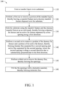
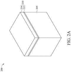
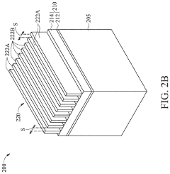
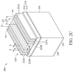
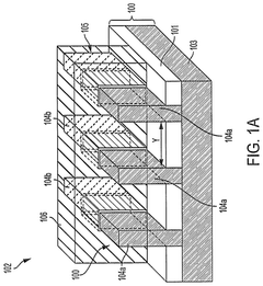
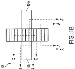
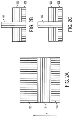
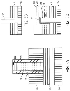
Fin-Like Field Effect Transistor Patterning Methods For Achieving Fin Width Uniformity
PatentPendingUS20230378330A1
Innovation
- The introduction of dummy fins adjacent to isolated active fins reduces left/right loading, enhancing fin width uniformity by maintaining density closer to that of dense active fins, thereby improving etching uniformity and reducing fin etch iso/dense loading effects.
Self aligned replacement metal source/drain finfet
PatentPendingUS20250142872A1
Innovation
- The method involves forming a fin-shaped field effect transistor (finFET) by creating a fin that extends in a first direction, covering it with a dummy gate stack, and then replacing it with a replacement metal gate stack, followed by a first anneal and subsequent formation of metallic source and drain regions.
Environmental Impact of Advanced Lithography Processes
The environmental impact of advanced lithography processes used in FinFET patterning has become increasingly significant as semiconductor manufacturing scales to smaller nodes. Extreme Ultraviolet (EUV) lithography, a key enabler for sub-7nm FinFET structures, presents a complex environmental profile. The process requires substantial energy consumption—approximately 40kW per tool—primarily due to the high-powered CO2 lasers needed to generate EUV light. A typical semiconductor fab utilizing multiple EUV systems can consume energy equivalent to that of a small town, contributing significantly to carbon emissions when powered by non-renewable sources.
Water usage represents another critical environmental concern. Advanced lithography processes for FinFET patterning require ultra-pure water (UPW) for cleaning and rinsing steps, with a single fab potentially consuming 2-4 million gallons daily. The purification process for this water is itself energy-intensive, creating a compound environmental impact. Additionally, the water discharged contains trace amounts of chemicals and metals that require specialized treatment before release.
Chemical consumption in advanced lithography presents further environmental challenges. EUV resists contain metal compounds that improve sensitivity but can be environmentally persistent. Multiple patterning techniques, often used alongside EUV for FinFET fabrication, require additional chemical steps including etching chemicals, developers, and strippers. Many of these substances have high global warming potential (GWP) or are classified as volatile organic compounds (VOCs).
Waste management represents a growing challenge as patterning techniques advance. The semiconductor industry generates significant amounts of hazardous waste from photoresist materials, developer solutions, and etching chemicals. The complex multi-patterning schemes required for advanced FinFET structures multiply these waste streams. Industry data suggests that for every square centimeter of processed wafer, approximately 1.5 grams of chemical waste is generated.
Recent industry initiatives have focused on developing more sustainable lithography approaches. These include the implementation of closed-loop systems for chemical recycling, which can reduce fresh chemical consumption by up to 30%. Energy efficiency improvements in newer generation EUV systems aim to reduce power consumption by 15-20% compared to first-generation tools. Additionally, alternative resist formulations with lower environmental persistence are being researched, though these must maintain the resolution capabilities required for advanced FinFET structures.
Regulatory frameworks worldwide are increasingly addressing these environmental concerns, with the European Union's Restriction of Hazardous Substances (RoHS) directive and similar regulations in Asia impacting material selection for lithography processes. Semiconductor manufacturers are responding by implementing environmental management systems and setting ambitious sustainability targets, including carbon neutrality goals and water recycling initiatives.
Supply Chain Resilience for Critical Patterning Materials
The resilience of the supply chain for critical patterning materials represents a significant concern in the advancement of FinFET technology. As semiconductor manufacturing continues to push the boundaries of scale and resolution, the dependence on specialized materials has intensified, creating potential vulnerabilities in the production ecosystem.
Critical patterning materials for FinFET fabrication include advanced photoresists, extreme ultraviolet (EUV) pellicles, and specialized etching chemicals. These materials often originate from limited geographical sources, with Japan, South Korea, and the United States dominating production. Recent geopolitical tensions and trade restrictions have highlighted the fragility of this supply network, prompting industry leaders to reconsider their sourcing strategies.
The COVID-19 pandemic further exposed weaknesses in the semiconductor supply chain, as manufacturing disruptions led to significant delays in chip production. For FinFET patterning specifically, the limited availability of high-purity chemicals and specialized photoresists created bottlenecks that reverberated throughout the industry. These disruptions demonstrated that even temporary shortages of critical materials can have long-lasting impacts on production schedules and technological advancement.
To address these vulnerabilities, leading semiconductor manufacturers have begun implementing multi-faceted resilience strategies. These include geographical diversification of suppliers, development of alternative materials with similar performance characteristics, and increased inventory buffers for critical components. TSMC, for instance, has expanded its supplier network across multiple regions while investing in research for material alternatives that could reduce dependence on scarce resources.
Material qualification represents another significant challenge in supply chain resilience. The introduction of new suppliers or alternative materials requires extensive testing and validation to ensure they meet the exacting standards required for advanced FinFET patterning. This process can take months or even years, creating a substantial barrier to rapid supply chain diversification.
Looking forward, the industry is exploring several innovative approaches to enhance supply chain resilience. These include the development of circular economy models for rare materials recovery, advanced predictive analytics for supply chain risk management, and collaborative industry initiatives to establish material standards that facilitate supplier interchangeability. Additionally, research into novel patterning techniques that utilize more readily available materials could potentially reduce dependence on critical supply-constrained resources while maintaining the scaling trajectory of FinFET technology.
Unlock deeper insights with PatSnap Eureka Quick Research — get a full tech report to explore trends and direct your research. Try now!
Generate Your Research Report Instantly with AI Agent
Supercharge your innovation with PatSnap Eureka AI Agent Platform!