

FinFET Sizing Analysis: Design Implications
SEP 11, 20259 MIN READ
Generate Your Research Report Instantly with AI Agent
PatSnap Eureka helps you evaluate technical feasibility & market potential.
FinFET Evolution and Design Objectives
The evolution of FinFET technology represents one of the most significant advancements in semiconductor manufacturing over the past two decades. Initially introduced by researchers at UC Berkeley in 1998, FinFETs emerged as a revolutionary solution to the scaling limitations of traditional planar transistors. The three-dimensional fin structure fundamentally changed how transistor channels are formed and controlled, enabling continued adherence to Moore's Law beyond the 22nm node where conventional transistors faced severe short-channel effects.
The technological progression of FinFETs has followed a clear trajectory of dimensional refinement. First-generation FinFETs featured relatively wide fins with heights of approximately 30-40nm. Subsequent generations have consistently reduced fin width while increasing height, moving from 22nm to 14nm, then to 10nm and 7nm nodes. This evolution has been driven by the need to enhance electrostatic control while maintaining or improving current drive capabilities.
A critical aspect of FinFET development has been the transition from bulk silicon substrates to silicon-on-insulator (SOI) implementations, each offering distinct advantages in terms of manufacturing complexity, parasitic capacitance, and thermal characteristics. The industry has also witnessed innovations in multi-fin configurations and the introduction of strain engineering techniques to enhance carrier mobility.
The primary technical objectives of modern FinFET sizing analysis center on optimizing the delicate balance between performance, power consumption, and area efficiency. As dimensions continue to shrink, designers face increasingly complex trade-offs between these parameters. Specifically, fin height, width, and pitch must be carefully calibrated to maximize current drive while minimizing leakage current and ensuring reliable operation.
Another key objective involves addressing quantum mechanical effects that become increasingly prominent at sub-10nm nodes. Electron tunneling, confinement effects, and variability due to random dopant fluctuations present significant challenges that require sophisticated modeling approaches and novel design methodologies.
Looking forward, the industry aims to extend FinFET technology to its physical limits before transitioning to alternative architectures such as gate-all-around (GAA) FETs. This extension requires innovations in materials science, including the integration of high-mobility channel materials like SiGe and III-V compounds, as well as advanced metal gates and high-k dielectrics.
The ultimate goal of current FinFET sizing analysis is to establish comprehensive design frameworks that can accurately predict device behavior across various operating conditions while accounting for manufacturing variability. These frameworks must enable designers to make informed decisions about transistor sizing that optimize circuit-level metrics including speed, power, and reliability.
Market Demand for Advanced Semiconductor Nodes
The semiconductor industry is witnessing unprecedented demand for advanced nodes, particularly those utilizing FinFET technology. This demand is primarily driven by the continuous push for higher performance, lower power consumption, and increased transistor density in electronic devices. Market research indicates that the global semiconductor industry is projected to reach $1 trillion by 2030, with advanced nodes accounting for a significant portion of this growth.
The demand for FinFET-based advanced nodes is particularly strong in several key sectors. In mobile computing, smartphone manufacturers require increasingly powerful yet energy-efficient processors to support advanced features like AI processing, high-resolution displays, and 5G connectivity while maintaining battery life. The data center market represents another major demand driver, as cloud service providers continuously seek to improve computational efficiency and reduce operational costs through more advanced semiconductor technologies.
Automotive electronics has emerged as a rapidly growing market segment for advanced nodes. The increasing integration of advanced driver-assistance systems (ADAS), infotainment systems, and the gradual shift toward autonomous vehicles necessitate more sophisticated semiconductor components with precise FinFET sizing to balance performance and power requirements.
Consumer electronics beyond smartphones, including tablets, wearables, and smart home devices, constitute another significant market segment demanding advanced semiconductor nodes. These applications often require specialized FinFET designs that prioritize either performance or power efficiency depending on the use case.
Market analysis reveals regional variations in demand patterns. Asia-Pacific, particularly Taiwan, South Korea, and increasingly China, dominates manufacturing capacity for advanced nodes, while North America leads in design innovation. Europe shows growing demand primarily driven by the automotive and industrial sectors.
The transition to each new node generation typically results in a 15-20% performance improvement and 25-30% power reduction, creating strong market incentives for adoption despite increasing development costs. Industry forecasts suggest that demand for 5nm and 3nm nodes will grow at a compound annual rate exceeding 30% through 2025, with early development already underway for 2nm and beyond.
Supply chain constraints and geopolitical factors have recently impacted market dynamics, creating both challenges and opportunities for different players in the ecosystem. The increasing complexity of FinFET sizing analysis at advanced nodes has also led to growing demand for specialized electronic design automation (EDA) tools and expertise, creating adjacent market opportunities in the semiconductor ecosystem.
Current FinFET Sizing Challenges and Limitations
Despite significant advancements in FinFET technology, current sizing methodologies face several critical challenges that limit optimal device performance and design efficiency. The fundamental issue stems from the three-dimensional nature of FinFET structures, which introduces complex electrostatic interactions not present in planar MOSFET designs. These interactions create non-intuitive relationships between device dimensions and electrical characteristics, complicating traditional sizing approaches.
One major limitation is the quantized nature of fin width adjustments. Unlike planar technologies where transistor width can be continuously varied, FinFET designs must add or remove entire fins, creating a stepped approach to current scaling. This quantization effect significantly constrains fine-grained performance tuning, particularly in analog and mixed-signal applications where precise current matching is essential.
The multi-fin configuration introduces additional challenges related to parasitic capacitance and resistance. As the number of fins increases, parasitic elements grow non-linearly, creating diminishing returns in performance improvement while exacerbating power consumption and switching delays. Current modeling tools struggle to accurately capture these effects across different process nodes and operating conditions.
Self-heating has emerged as another critical limitation in advanced FinFET nodes. The confined geometry of fins restricts efficient heat dissipation, causing localized temperature increases that alter device characteristics during operation. This thermal feedback loop creates time-dependent performance variations that are difficult to predict during the design phase, leading to reliability concerns and potential circuit failures.
Process variation presents perhaps the most significant challenge to consistent FinFET sizing. Manufacturing tolerances in fin height, width, and gate length create substantial device-to-device variability, particularly at sub-7nm nodes. These variations manifest as threshold voltage shifts and drive current inconsistencies that can undermine carefully optimized designs. Current statistical models often fail to capture the full complexity of these variations, especially their spatial correlation patterns.
Layout-dependent effects further complicate sizing strategies. Proximity effects between adjacent FinFETs, well proximity effects, and stress-induced variations can significantly alter device performance based on their physical arrangement. These effects create a complex interdependence between circuit layout and device sizing that traditional design flows struggle to address effectively.
The industry also faces challenges with existing design tools, many of which were originally developed for planar technologies and subsequently adapted for FinFETs. These tools often employ simplified models that fail to capture the full complexity of three-dimensional electrostatics, particularly in advanced nodes where quantum effects become increasingly significant.
Current FinFET Sizing Methodologies
01 FinFET dimension optimization techniques
Various techniques for optimizing the dimensions of FinFETs to achieve desired performance characteristics. This includes adjusting fin height, width, and pitch to control current drive, leakage, and power consumption. The optimization process often involves simulation tools that can predict device performance based on dimensional parameters, allowing for precise sizing to meet specific application requirements.- FinFET dimension optimization techniques: Various techniques for optimizing the dimensions of FinFET devices to achieve desired performance characteristics. This includes adjusting fin height, width, and pitch to control parameters such as current drive, leakage, and threshold voltage. Proper sizing of these dimensions is critical for balancing performance and power consumption in advanced semiconductor nodes.
- Multi-fin FinFET design considerations: Design methodologies for multi-fin FinFET structures that address how to determine the optimal number of fins and their arrangement. This includes considerations for parallel fin configurations, spacing between fins, and how these parameters affect device characteristics such as drive current, capacitance, and switching speed. Multi-fin designs allow for scalable performance based on application requirements.
- FinFET sizing for specific applications: Specialized sizing approaches for FinFETs targeted at specific applications such as low power, high performance, or mixed-signal circuits. Different applications require different optimization priorities, such as minimizing leakage for mobile devices or maximizing drive strength for high-performance computing. These approaches include adjusting fin dimensions and device layout to meet application-specific requirements.
- Automated FinFET sizing and optimization tools: Computer-aided design tools and methodologies for automating the sizing and optimization of FinFET devices. These tools incorporate models that predict device performance based on dimensional parameters and can automatically determine optimal sizing for given design constraints. They enable efficient exploration of the design space and reduce time-to-market for FinFET-based integrated circuits.
- Advanced FinFET sizing for next-generation nodes: Cutting-edge approaches for sizing FinFETs at advanced technology nodes (5nm and below), addressing challenges such as quantum effects, variability, and reliability concerns. These techniques include novel fin shapes, materials, and configurations to maintain performance scaling while managing increasing physical limitations. They represent the frontier of FinFET development for future semiconductor technologies.
02 Multi-fin FinFET configurations
Design approaches for multi-fin FinFET structures where multiple fins are used to increase current drive capability. These configurations require careful sizing considerations for each fin and the spacing between fins to optimize performance while maintaining manufacturability. The number of fins can be adjusted based on the required drive strength, with proper sizing ensuring uniform current distribution across all fins.Expand Specific Solutions03 Gate length and width considerations
Specific approaches to determining optimal gate dimensions in FinFET devices. The gate length affects channel control and short-channel effects, while gate width (effectively determined by fin height and number) affects current drive. Proper sizing of these parameters is crucial for balancing performance, power consumption, and area efficiency in FinFET-based integrated circuits.Expand Specific Solutions04 FinFET sizing for specific applications
Tailored sizing methodologies for FinFETs in different application contexts such as memory, logic, or analog circuits. Each application has unique requirements for performance, power, and area that influence the optimal FinFET dimensions. The sizing approaches consider factors like operating voltage, frequency targets, and noise margins to determine the most suitable fin dimensions and configurations.Expand Specific Solutions05 Advanced FinFET sizing methodologies
Novel approaches and methodologies for FinFET sizing that go beyond conventional techniques. These include machine learning-based optimization, automated design space exploration, and physics-based modeling to determine optimal dimensions. These advanced methodologies aim to address challenges in nanoscale FinFET design where traditional sizing rules may not be sufficient to achieve the desired balance of performance, power, and reliability.Expand Specific Solutions
Key Semiconductor Players and Foundries
The FinFET sizing analysis market is currently in a mature growth phase, with the technology becoming standard in advanced semiconductor manufacturing. The global market size for FinFET technology exceeds $40 billion, driven by increasing demand for high-performance computing and mobile applications. In terms of technical maturity, industry leaders Taiwan Semiconductor Manufacturing Co. (TSMC) and Samsung Electronics have achieved commercial production at 5nm and below, while GlobalFoundries, Intel, and SMIC are at various stages of implementation. TSMC maintains technological leadership with the most advanced FinFET processes, while Samsung closely competes in cutting-edge nodes. Other players including UMC and Qualcomm focus on specialized applications of FinFET technology, creating a competitive landscape dominated by a few major foundries but with significant innovation occurring across the ecosystem.
Taiwan Semiconductor Manufacturing Co., Ltd.
Technical Solution: TSMC has pioneered advanced FinFET sizing methodologies through their comprehensive design technology co-optimization (DTCO) approach. Their N5 and N3 process nodes implement multi-fin optimization techniques where fin height, width, and pitch are precisely calibrated to balance performance and power consumption. TSMC's approach involves sophisticated simulation models that account for quantum confinement effects and mechanical stress in nanoscale FinFETs. Their methodology includes statistical variability analysis that addresses random dopant fluctuation (RDF) and line edge roughness (LER) to ensure design robustness. TSMC has developed specialized design rules and process design kits (PDKs) that incorporate FinFET-specific parameters such as effective channel width quantization and parasitic capacitance modeling to enable accurate circuit simulation[1][3]. Their sizing analysis framework integrates electrostatic integrity considerations with performance metrics to optimize transistor dimensions for specific application domains.
Strengths: Industry-leading process control enabling precise fin dimensions with minimal variability; comprehensive PDKs that accurately model FinFET behavior; advanced multi-patterning techniques allowing for tighter fin pitches. Weaknesses: Higher manufacturing costs associated with complex FinFET optimization; design constraints due to fin quantization limiting analog circuit flexibility; increased sensitivity to process variations at extreme scaling nodes.
Semiconductor Manufacturing International (Shanghai) Corp.
Technical Solution: SMIC has developed a pragmatic approach to FinFET sizing analysis focused on optimizing manufacturability and yield while maintaining competitive performance metrics. Their 14nm FinFET process incorporates specialized design rules that balance fin dimensions with process window considerations. SMIC's methodology includes comprehensive statistical analysis of process variations and their impact on circuit performance, enabling designers to implement robust sizing strategies that account for manufacturing realities. Their approach emphasizes the relationship between fin height-to-width ratio and electrostatic control, providing designers with guidelines for selecting optimal dimensions based on application requirements[5]. SMIC has implemented a unique "performance binning" strategy that allows for post-manufacturing optimization of circuit performance through selective voltage assignment based on measured FinFET characteristics. Their sizing analysis framework incorporates detailed parasitic extraction models calibrated specifically for their FinFET process, enabling accurate circuit simulation across various operating conditions. SMIC's methodology also addresses reliability considerations such as hot carrier injection (HCI) and bias temperature instability (BTI) through lifetime-aware sizing recommendations.
Strengths: Cost-effective manufacturing approach making FinFET technology more accessible; practical design guidelines optimized for yield; robust variation-aware sizing methodologies. Weaknesses: Less aggressive dimensional scaling compared to industry leaders; higher variability in certain electrical parameters; more conservative performance specifications.
Critical Patents in FinFET Dimension Optimization
Fin field-effect transistor having counter-doped regions between lightly doped regions and doped source/drain regions
PatentActiveUS11114551B2
Innovation
- A method involving lightly doped regions and counter doped regions formed through specific ion implantation processes to reduce the ion concentration gradient between doped source/drain regions and lightly doped regions, thereby mitigating the GIDL phenomenon.
Method of designing fin-based transistor for power optimization
PatentActiveTW201600988A
Innovation
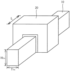
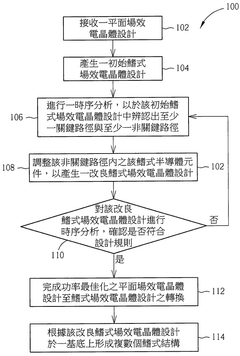
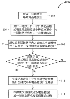
- A method is provided to design a fin structure transistor by identifying critical and non-critical paths in the initial FinFET design through timing analysis, and adjusting fin semiconductor elements in non-critical paths to reduce the number, width, or electrical connections of fins, thereby reducing power consumption.

Power-Performance-Area Trade-offs
The optimization of FinFET sizing represents a critical design challenge that directly impacts the power-performance-area (PPA) trade-offs in modern semiconductor devices. When analyzing these trade-offs, designers must carefully balance competing objectives that often pull in opposite directions.
Power consumption in FinFET designs can be categorized into dynamic and static components. Dynamic power scales with switching frequency, capacitance, and the square of supply voltage, while static power is dominated by leakage currents. FinFET sizing significantly influences both components - wider fins increase drive current but also increase dynamic power consumption, while taller fins can reduce short-channel effects but may increase parasitic capacitance.
Performance metrics, primarily measured through switching speed and delay characteristics, demonstrate a complex relationship with FinFET dimensions. Increasing the number of fins enhances drive current and improves performance, but this improvement follows a law of diminishing returns. Experimental data indicates that beyond a certain point, adding more fins yields minimal performance gains while continuing to increase power consumption and area requirements.
Area efficiency remains a paramount concern in semiconductor scaling. The quantized nature of FinFET width (determined by the number of fins) creates unique area optimization challenges compared to planar technologies. Multi-fin devices consume proportionally more silicon real estate, necessitating careful consideration of fin count versus performance benefits. Recent industry trends show that optimizing fin height can provide performance improvements without proportional area penalties.
The interdependence of these three factors creates a complex design space. For example, reducing supply voltage dramatically decreases power consumption but negatively impacts performance. Similarly, reducing fin count saves area but may require compensatory measures like increased channel doping that can degrade carrier mobility.
Advanced design methodologies now employ sophisticated multi-variable optimization techniques to navigate these trade-offs. Machine learning algorithms have demonstrated particular promise in identifying non-intuitive sizing configurations that maximize performance within strict power and area constraints. These approaches typically involve characterizing thousands of potential sizing combinations across various operating conditions.
Industry benchmarks suggest that optimal FinFET sizing can yield up to 30% power reduction or 25% performance improvement compared to non-optimized designs within the same area constraints. However, these benefits are highly dependent on the specific application requirements and process technology node.
Manufacturing Yield Considerations
Manufacturing yield is a critical factor in the economic viability of FinFET technology implementation. As device dimensions continue to shrink below 10nm, process variations become increasingly significant, directly impacting the manufacturing yield of FinFET-based integrated circuits. The relationship between FinFET sizing and yield considerations represents a complex optimization challenge that requires careful analysis and strategic decision-making.
Process variations in FinFET manufacturing manifest in several dimensions, including fin width fluctuations, gate length variations, and oxide thickness inconsistencies. These variations can lead to significant deviations in threshold voltage, drive current, and leakage characteristics across a wafer. Statistical analysis reveals that a mere 1nm variation in fin width can result in up to 15% threshold voltage variation, dramatically affecting circuit performance and power consumption profiles.
Yield optimization strategies for FinFET sizing must consider the trade-offs between performance targets and manufacturing robustness. Larger FinFET dimensions generally improve manufacturing yield but may compromise performance density advantages. Conversely, aggressive scaling enhances performance but increases sensitivity to process variations, potentially reducing yield. Advanced foundries typically implement design-for-manufacturing (DFM) guidelines that specify minimum fin widths and gate lengths to ensure acceptable yield levels.
Redundancy techniques have emerged as effective approaches to mitigate yield concerns in FinFET designs. These include implementing spare fins that can be selectively activated post-manufacturing to compensate for defective structures. Additionally, adaptive body biasing techniques allow for post-silicon tuning to counteract process variations, thereby salvaging otherwise non-functional chips and improving overall yield metrics.
Economic considerations further complicate the FinFET sizing decision process. While smaller dimensions theoretically allow for more dies per wafer, the associated yield reduction may negate this advantage. Cost modeling indicates that the optimal FinFET sizing from a yield perspective often differs from what would be ideal for pure performance considerations. Industry data suggests that a 5-10% increase in critical dimensions can result in yield improvements of up to 30% in early technology nodes, representing significant cost savings.
Advanced metrology and inspection techniques have become essential components of yield management for FinFET manufacturing. In-line monitoring of critical dimensions, combined with machine learning algorithms for defect classification, enables rapid feedback loops for process adjustment. These systems can detect subtle pattern dependencies that affect yield, allowing for design rule modifications that improve manufacturability without compromising essential performance characteristics.
Unlock deeper insights with PatSnap Eureka Quick Research — get a full tech report to explore trends and direct your research. Try now!
Generate Your Research Report Instantly with AI Agent
Supercharge your innovation with PatSnap Eureka AI Agent Platform!