FinFET Vs FD-SOI: Speed Efficiency In IoT Devices
SEP 11, 20259 MIN READ
Generate Your Research Report Instantly with AI Agent
Patsnap Eureka helps you evaluate technical feasibility & market potential.
FinFET and FD-SOI Evolution for IoT Applications
The evolution of FinFET and FD-SOI technologies represents a significant paradigm shift in semiconductor manufacturing, particularly for IoT applications. FinFET (Fin Field-Effect Transistor) emerged around 2011 when Intel introduced its 22nm 3D transistor technology, marking the first commercial deployment of non-planar transistors. This three-dimensional structure allowed for better control of electrical current, significantly reducing leakage and enabling continued scaling beyond the limitations of planar transistors.
FD-SOI (Fully Depleted Silicon On Insulator), meanwhile, evolved as an alternative approach, with companies like STMicroelectronics and GlobalFoundries championing its development. FD-SOI utilizes an ultra-thin layer of silicon over an insulator, offering unique advantages in power management through body biasing capabilities that became particularly relevant for IoT applications.
The technological trajectories of these architectures have been shaped by different market demands. FinFET development has been primarily driven by high-performance computing needs, with successive generations (14nm, 10nm, 7nm, and beyond) focusing on transistor density and raw performance. This evolution path has been dominated by industry leaders like TSMC, Samsung, and Intel.
FD-SOI has evolved along a different trajectory, with its development focusing on optimizing the balance between performance and power efficiency. The technology has progressed from 28nm to 22nm and now to 18nm nodes, with each generation enhancing the body biasing capabilities and reducing operating voltage, making it increasingly suitable for energy-constrained IoT devices.
For IoT applications specifically, the evolution has been characterized by divergent optimization strategies. FinFET technology has been adapted for IoT through specialized low-power process variants that sacrifice some performance for reduced power consumption. Meanwhile, FD-SOI has evolved with IoT as a primary target market, with features like wide voltage range operation and excellent analog/RF performance being continuously enhanced.
Recent developments show both technologies continuing to evolve for IoT needs. FinFET is moving toward gate-all-around structures and vertical nanosheets to further improve electrostatic control at smaller nodes, while FD-SOI is advancing with enhanced body biasing techniques and ultra-low leakage optimizations. The industry is witnessing a convergence where aspects of both technologies are being combined in hybrid approaches to address the diverse requirements of next-generation IoT devices.
This technological evolution reflects the semiconductor industry's response to the unique challenges of IoT applications, where devices must balance computational capabilities with stringent power constraints across widely varying workloads and operating environments.
IoT Market Demands for Energy-Efficient Processors
The Internet of Things (IoT) market is experiencing unprecedented growth, with projections indicating a global market value exceeding $1.5 trillion by 2025. This expansion is driving significant demand for processors that can deliver optimal performance while maintaining minimal energy consumption. Energy efficiency has emerged as the paramount requirement for IoT devices, surpassing even raw processing power in importance for many applications.
The diverse IoT ecosystem encompasses devices ranging from simple sensors to complex edge computing systems, each with unique power constraints. Battery-powered devices, which constitute over 70% of IoT endpoints, particularly demand ultra-low-power processors to extend operational life between charges or battery replacements. Market research indicates that extending battery life by even 20% can reduce total ownership costs by up to 30% for large-scale IoT deployments.
Consumer and industrial IoT segments are driving distinct processor requirements. Consumer IoT devices prioritize cost-effectiveness and adequate performance for specific tasks, while industrial applications demand reliability and consistent performance under varying environmental conditions. Both segments, however, share the critical need for energy efficiency as a fundamental design parameter.
Real-time processing capabilities are becoming increasingly important as IoT applications evolve. The ability to process data locally rather than transmitting it to cloud servers not only reduces latency but also significantly decreases power consumption associated with wireless communication. This trend toward edge computing is reshaping processor requirements, with energy-efficient local processing becoming a key differentiator in the market.
Security features integrated into processors are gaining prominence as IoT devices become more prevalent in critical infrastructure and personal environments. However, these security implementations must be designed with energy efficiency in mind, as traditional security protocols can substantially increase power consumption.
Form factor constraints present another significant market demand. As IoT devices continue to shrink in size, processors must deliver increased performance density—more computing power per unit of energy consumed. This trend is particularly evident in wearable technology and environmental sensors, where physical dimensions are severely limited.
The market is also showing increased interest in processors that can dynamically adjust performance based on workload, optimizing energy usage in real-time. This adaptive capability allows devices to conserve power during periods of low activity while maintaining the ability to handle processing spikes when needed, representing an ideal balance for IoT applications with variable workloads.
Technical Comparison and Challenges Between FinFET and FD-SOI
FinFET and FD-SOI represent two distinct approaches to transistor architecture in advanced semiconductor manufacturing. FinFET (Fin Field-Effect Transistor) utilizes a three-dimensional fin-like structure that extends vertically from the substrate, allowing for better control of electrical current flow. This design significantly reduces leakage current and enables higher performance at lower voltages. In contrast, FD-SOI (Fully Depleted Silicon On Insulator) employs a thin layer of silicon positioned on top of an insulator, creating a fully depleted channel that enhances electron mobility and reduces parasitic capacitance.
From a technical perspective, FinFET demonstrates superior performance characteristics in high-performance computing scenarios, delivering faster switching speeds and higher drive currents. The multi-gate structure provides excellent electrostatic control, allowing for effective scaling to smaller nodes (7nm and below). However, this architecture introduces manufacturing complexities due to its three-dimensional structure, requiring sophisticated lithography techniques and precise fin formation processes.
FD-SOI, while generally offering lower peak performance than FinFET, excels in power efficiency through its inherent body-biasing capability. This feature allows for dynamic voltage adjustment, enabling significant power savings in low-power operation modes - a critical advantage for IoT devices with stringent power constraints. The planar structure of FD-SOI also simplifies the manufacturing process compared to FinFET, potentially reducing production costs and improving yield rates.
A key technical challenge for FinFET implementation in IoT devices stems from its relatively higher static power consumption. Despite improvements in leakage current control, the complex fin structure introduces additional junction areas that contribute to standby power drain - problematic for battery-powered IoT applications requiring extended operational lifetimes.
For FD-SOI, the primary technical limitation lies in its scalability beyond certain process nodes. While effective at 28nm and 22nm nodes commonly used for IoT applications, FD-SOI faces increasing difficulties at more advanced nodes where FinFET maintains better electrostatic control. Additionally, the ultra-thin silicon layer in FD-SOI presents manufacturing uniformity challenges that can impact device performance consistency.
Radio frequency (RF) performance represents another critical comparison point for IoT applications. FD-SOI demonstrates superior RF characteristics due to lower parasitic capacitance and reduced substrate coupling effects, making it particularly suitable for wireless IoT devices. FinFET, while offering excellent digital performance, typically requires additional engineering to achieve comparable RF capabilities.
Temperature sensitivity also differs significantly between these technologies. FinFET maintains more stable performance across temperature variations, while FD-SOI exhibits greater performance fluctuations with temperature changes - a consideration for IoT devices deployed in diverse environmental conditions.
Current Implementation Solutions for IoT SoCs
01 FinFET architecture for improved speed efficiency
FinFET technology offers superior speed efficiency through its three-dimensional structure that provides better channel control. The fin-shaped channel allows for reduced short-channel effects and lower leakage currents, resulting in faster switching speeds and improved performance at lower operating voltages. The multi-gate design enhances electrostatic control of the channel, leading to better subthreshold swing and higher drive currents, which directly contributes to increased processing speed in integrated circuits.- FinFET architecture for improved speed efficiency: FinFET technology offers superior speed efficiency through its three-dimensional structure that provides better channel control. The fin-shaped channel allows for reduced short-channel effects and lower leakage currents, resulting in faster switching speeds and improved performance at lower operating voltages. The multi-gate design enhances electrostatic control of the channel, leading to better subthreshold swing and higher drive currents, which directly contributes to increased operational speed in integrated circuits.
- FD-SOI technology advantages for power-efficient performance: Fully Depleted Silicon-On-Insulator (FD-SOI) technology provides significant advantages for speed-efficient applications through its ultra-thin silicon layer on an insulator. This architecture reduces parasitic capacitances and junction leakage, enabling faster switching speeds while consuming less power. FD-SOI allows for effective body biasing techniques that can dynamically optimize performance or power consumption based on workload requirements, making it particularly suitable for applications requiring both high speed and energy efficiency.
- Comparative performance analysis between FinFET and FD-SOI: When comparing FinFET and FD-SOI technologies for speed efficiency, each offers distinct advantages depending on application requirements. FinFETs generally provide higher performance at advanced nodes with better scalability, while FD-SOI excels in power efficiency and analog/RF performance. The choice between these technologies involves trade-offs between maximum processing speed, power consumption, manufacturing complexity, and cost considerations. For high-performance computing applications, FinFETs may offer superior speed, while FD-SOI might be preferred for applications requiring balanced performance and power efficiency.
- Circuit design optimization techniques for FinFET and FD-SOI: Optimizing circuit designs specifically for FinFET or FD-SOI technologies can significantly enhance speed efficiency. For FinFETs, techniques include optimizing fin height and width, gate length scaling, and multi-fin configurations to maximize drive current. For FD-SOI, design optimizations focus on body bias techniques, ultra-thin channel engineering, and reduced parasitic capacitances. Advanced layout techniques, transistor sizing methodologies, and circuit topologies tailored to the unique characteristics of each technology can further improve switching speeds and overall performance efficiency.
- Integration challenges and solutions for speed-optimized implementations: Implementing speed-optimized FinFET and FD-SOI technologies presents various integration challenges that require innovative solutions. These include managing increased process complexity, addressing variability issues, optimizing contact resistance, and ensuring thermal management. Advanced solutions involve novel materials integration, improved doping techniques, enhanced lithography processes, and specialized interconnect strategies. Hybrid approaches that combine elements of both technologies are also being explored to maximize speed efficiency while mitigating the limitations inherent to each technology individually.
02 FD-SOI technology advantages for power efficiency
Fully Depleted Silicon-On-Insulator (FD-SOI) technology provides significant power efficiency benefits through its ultra-thin silicon layer on an insulator substrate. This architecture reduces parasitic capacitances and junction leakage, enabling lower power consumption while maintaining high performance. FD-SOI allows for effective body biasing techniques that can dynamically optimize the power-performance trade-off, making it particularly suitable for applications requiring both high speed and energy efficiency. The technology's inherent radiation hardness also makes it valuable for specialized high-reliability applications.Expand Specific Solutions03 Comparative performance analysis between FinFET and FD-SOI
When comparing FinFET and FD-SOI technologies, each offers distinct advantages for speed efficiency. FinFETs generally provide higher performance at advanced nodes but with increased manufacturing complexity. FD-SOI delivers excellent performance at moderate nodes with simpler manufacturing processes and superior low-power operation. The choice between these technologies depends on specific application requirements, with FinFETs typically excelling in high-performance computing scenarios while FD-SOI offers better efficiency for mobile and IoT applications where power consumption is critical.Expand Specific Solutions04 Circuit design optimization techniques for FinFET and FD-SOI
Optimizing circuit designs specifically for FinFET or FD-SOI technologies can significantly enhance speed efficiency. For FinFETs, techniques include optimizing fin height and width, gate length scaling, and multi-threshold voltage designs. For FD-SOI, forward body biasing, ultra-thin body and box optimization, and specialized layout techniques maximize performance. Advanced design methodologies like multi-Vt libraries and adaptive body biasing schemes allow designers to leverage the unique characteristics of each technology to achieve optimal speed-power trade-offs in various application scenarios.Expand Specific Solutions05 Integration challenges and future developments
Both FinFET and FD-SOI technologies face integration challenges that impact speed efficiency. These include managing parasitic capacitances, addressing variability issues, and ensuring reliable contacts and interconnects. Future developments focus on vertical transistor architectures, gate-all-around structures, and novel channel materials to further enhance speed efficiency. Research is also exploring hybrid approaches that combine aspects of both technologies to leverage their respective advantages. Continued scaling and material innovations aim to overcome current limitations and push the boundaries of semiconductor performance.Expand Specific Solutions
Leading Semiconductor Manufacturers in IoT Chipsets
The IoT device market is witnessing a critical technological competition between FinFET and FD-SOI architectures, currently in a growth phase with expanding market opportunities. While FinFET technology, championed by industry leaders like TSMC, Samsung, and GlobalFoundries, offers superior performance for high-computing applications, FD-SOI (promoted by STMicroelectronics and Samsung) provides better power efficiency crucial for IoT devices. The market is projected to reach $25 billion by 2025, with companies increasingly adopting hybrid approaches. TSMC and Samsung maintain technological leadership, while IBM and GlobalFoundries continue advancing both technologies through significant R&D investments, creating a competitive landscape where specialized solutions are emerging for different IoT application segments.
Taiwan Semiconductor Manufacturing Co., Ltd.
Technical Solution: TSMC has developed advanced FinFET technology down to 3nm with their N3 process, offering significant power efficiency improvements for IoT applications. Their FinFET solutions provide up to 70% power reduction compared to planar transistors while maintaining high performance. For IoT-specific applications, TSMC offers specialized ultra-low power (ULP) FinFET processes that operate at lower voltages (0.5V) while maintaining performance integrity. Their N12e process specifically targets IoT edge computing with optimized power-performance balance. TSMC's approach focuses on scaling FinFET technology to address the diverse requirements of IoT devices, from high-performance edge computing to ultra-low power sensors[1][3].
Strengths: Industry-leading process technology with proven reliability and performance; extensive ecosystem support; superior power efficiency at advanced nodes. Weaknesses: Higher manufacturing costs compared to FD-SOI; more complex fabrication process requiring sophisticated equipment; potentially less suitable for extremely low-power IoT applications where cost is a primary constraint.
GLOBALFOUNDRIES, Inc.
Technical Solution: GlobalFoundries has positioned itself as the leader in FD-SOI technology with their 22FDX platform specifically designed for IoT applications. Their FD-SOI solution enables body-biasing techniques that allow dynamic adjustment of power-performance tradeoffs at runtime, achieving up to 50% lower power consumption compared to equivalent FinFET implementations. The 22FDX platform delivers FinFET-class performance (up to 450MHz) while consuming 30-50% less power, making it particularly suitable for battery-powered IoT devices. GlobalFoundries' technology enables operation at voltages as low as 0.4V, with the ability to integrate RF, analog, and embedded memory on the same chip, reducing overall system complexity and cost. Their roadmap includes scaling to 12FDX to further improve performance while maintaining power efficiency advantages[2][5].
Strengths: Superior power efficiency at moderate performance levels; excellent RF integration capabilities; body-biasing flexibility for dynamic power management; lower manufacturing costs than FinFET. Weaknesses: Performance limitations compared to leading-edge FinFET at high-computing workloads; smaller ecosystem compared to mainstream FinFET technologies; limited to less aggressive scaling paths.
Key Patents and Innovations in Low-Power Transistor Design
Approach for an Area-Efficient and Scalable CMOS Performance Based on Advanced Silicon-On-Insulator (SOI), Silicon-On-Sapphire (SOS) and Silicon-On-Nothing (SON) Technologies
PatentInactiveUS20170358686A1
Innovation
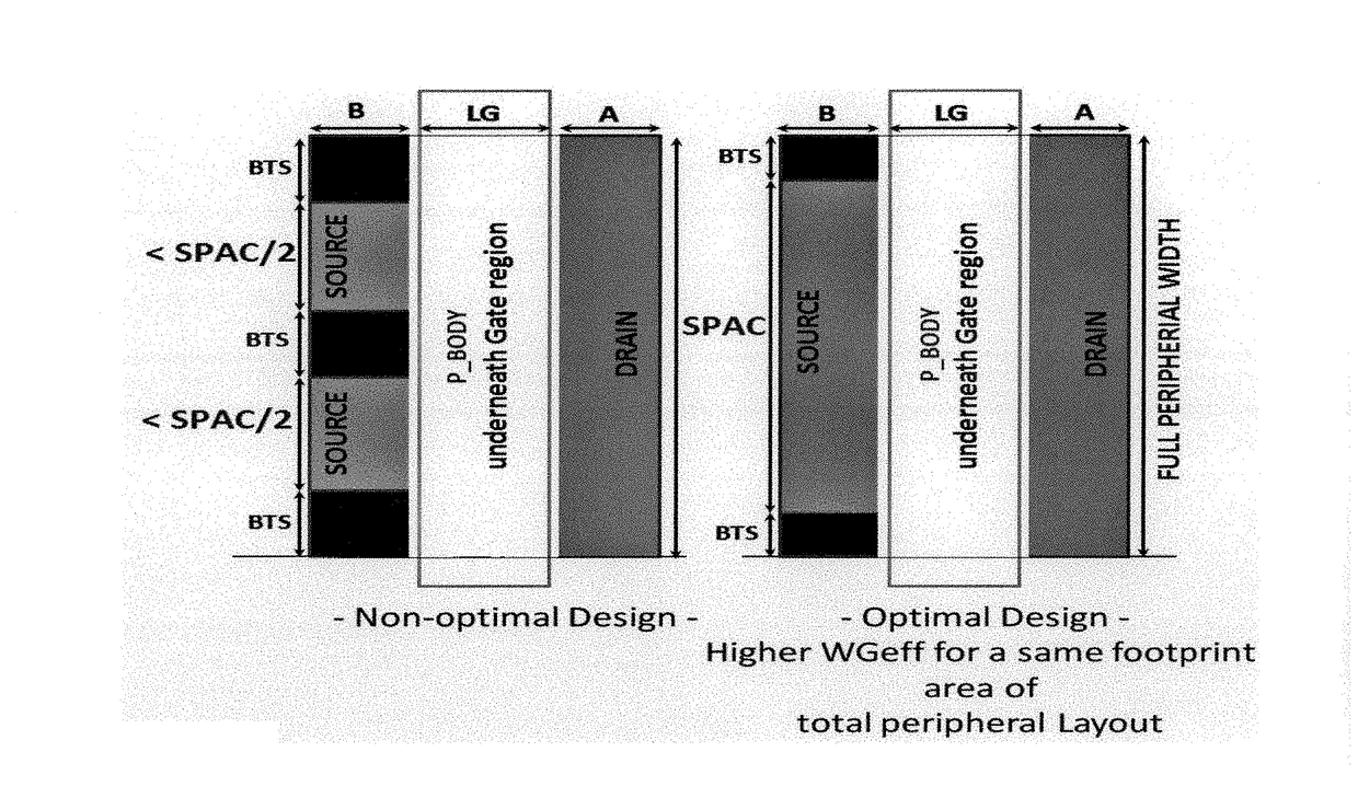
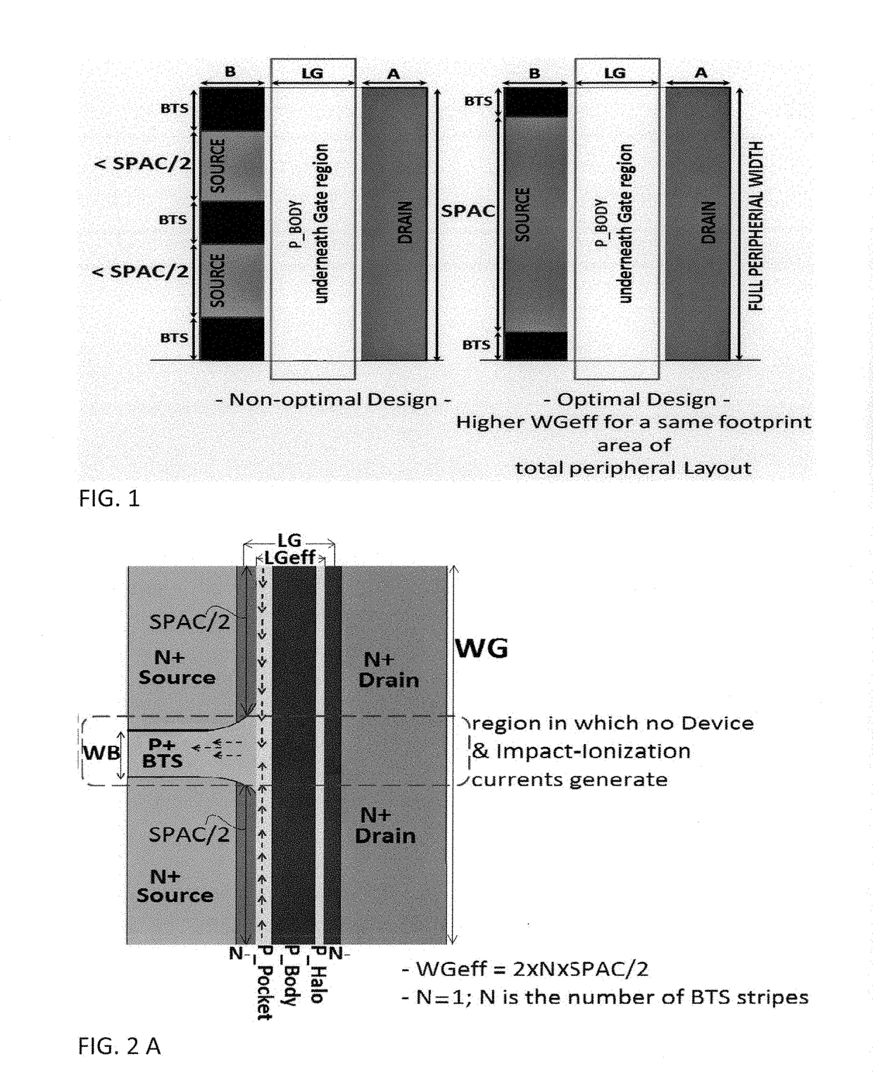
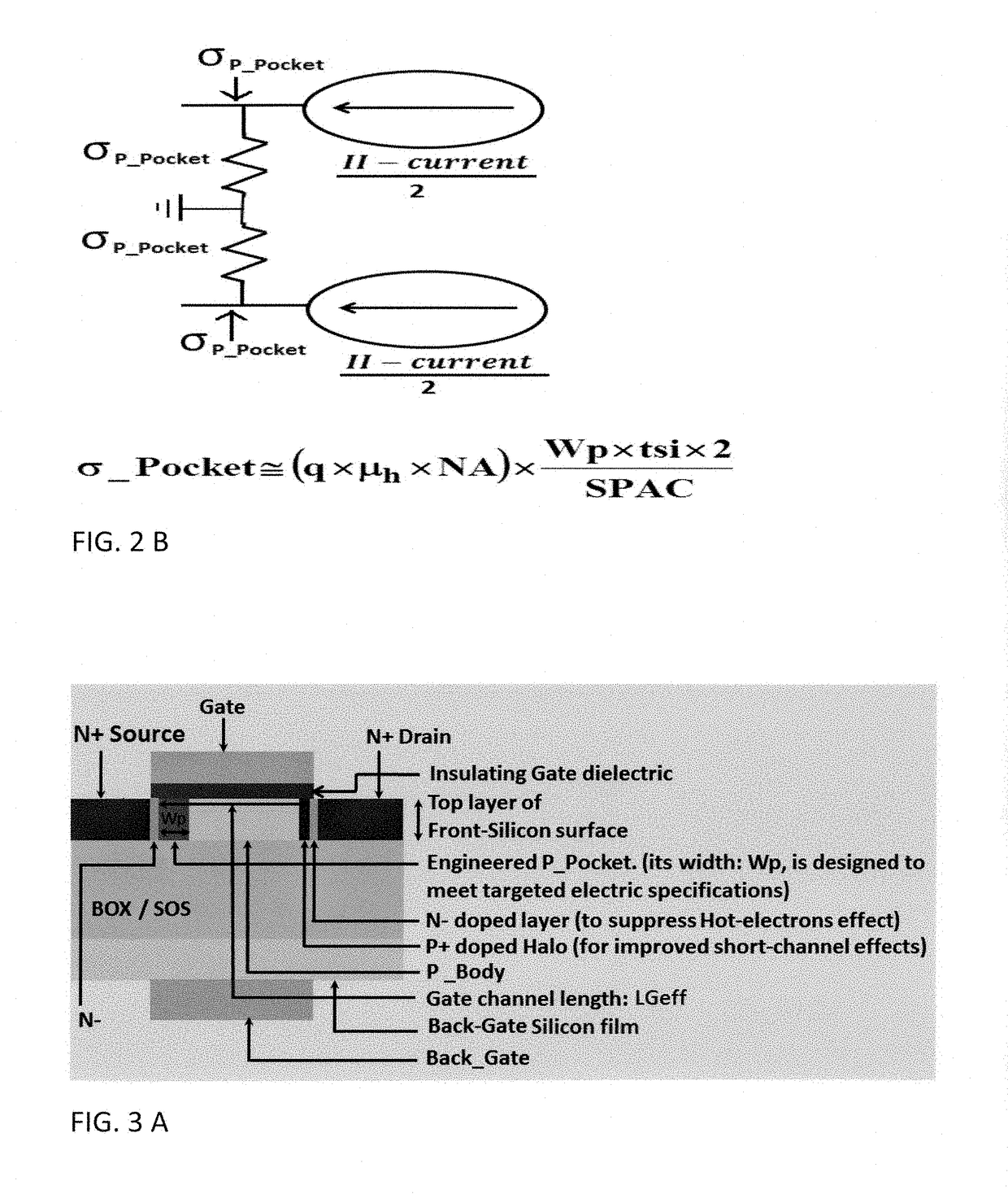
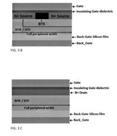
- The introduction of a highly conductive P-doped pocket between the Body and the Body-Tied-Source (BTS) structure, which enhances conductance and filters out Impact-Ionizations current, allowing the device to operate at high bias without activating parasitic Bipolar current, and incorporates a narrow BTS stripe configuration for area efficiency.
FinFET body contact structure
PatentInactiveUS7696565B2
Innovation
- A method and structure for creating a body contact in FinFETs using a polysilicon polygon shape with a center area without polysilicon, separated by a thin oxide layer, allowing for an electrical path wider than the channel length to couple the FinFET body to a voltage supply or another FinFET body, preventing silicide bridges by avoiding bridging vertices.
Manufacturing Cost Analysis of FinFET vs FD-SOI
Manufacturing cost analysis is a critical factor in determining the commercial viability of semiconductor technologies. When comparing FinFET and FD-SOI technologies for IoT device applications, several cost factors significantly impact the final manufacturing expenses and ultimately influence market adoption rates.
FinFET manufacturing processes typically require more complex lithography steps due to their three-dimensional fin structure. This complexity translates to higher capital equipment investments, with advanced FinFET production lines costing upwards of $10-15 billion to establish. The multi-patterning techniques required for sub-10nm FinFET nodes further escalate costs, with each additional mask layer adding approximately $5-7 million to the production expenses.
In contrast, FD-SOI manufacturing leverages a simpler planar structure that requires fewer lithography steps. The initial wafer cost for FD-SOI is higher due to the specialized silicon-on-insulator substrate, with raw SOI wafers costing 2-3 times more than bulk silicon wafers used in conventional processes. However, this is partially offset by reduced process complexity and fewer manufacturing steps.
Yield rates significantly impact overall manufacturing economics. FinFET processes typically experience lower initial yield rates (60-70%) compared to FD-SOI (75-85%) due to their structural complexity. This yield differential can represent a 10-15% cost advantage for FD-SOI in early production phases, though FinFET yields improve with manufacturing maturity.
Production volume considerations also favor different technologies. FinFET manufacturing demonstrates stronger economies of scale, making it more cost-effective for high-volume production exceeding millions of units. FD-SOI offers better cost efficiency for medium-volume production runs typical of specialized IoT applications, with the break-even point occurring at approximately 500,000 to 1 million units.
Energy consumption during manufacturing presents another cost differential. FinFET fabrication consumes approximately 30-40% more energy per wafer compared to FD-SOI processes, contributing to higher operational expenses in regions with elevated energy costs.
When analyzing total cost of ownership, FD-SOI demonstrates a 15-25% manufacturing cost advantage for IoT applications requiring 22-28nm nodes. However, for advanced nodes below 10nm where performance requirements are paramount, FinFET's higher manufacturing costs are often justified by superior performance characteristics despite the 30-40% cost premium.
Thermal Management Considerations for IoT Edge Devices
Thermal management represents a critical consideration when comparing FinFET and FD-SOI technologies for IoT edge devices. The architectural differences between these transistor technologies directly impact their thermal characteristics and power dissipation profiles, which significantly influences device performance and reliability in IoT deployments.
FinFET devices, with their 3D fin structure, typically generate more localized heat due to their higher current densities and more concentrated power dissipation. This can create thermal hotspots that require sophisticated cooling solutions, potentially challenging for space-constrained IoT edge devices. The vertical fin structure, while enabling higher performance, also presents unique thermal conductivity paths that must be carefully managed.
FD-SOI technology, by contrast, offers inherently better thermal characteristics for many IoT applications. The fully depleted silicon-on-insulator structure provides superior thermal isolation, reducing heat transfer to adjacent components. This characteristic is particularly valuable in densely packed IoT edge devices where component proximity can exacerbate thermal issues.
Power efficiency differences between these technologies directly influence thermal management requirements. FD-SOI's lower operating voltages and reduced leakage current translate to lower overall heat generation, often eliminating the need for active cooling solutions in IoT edge deployments. This passive cooling compatibility makes FD-SOI particularly attractive for battery-powered or energy-harvesting IoT devices.
Environmental considerations further complicate thermal management decisions. IoT edge devices frequently operate in uncontrolled environments with temperature extremes, requiring robust thermal design. FinFET's performance advantages may be offset by thermal challenges in high-temperature industrial or outdoor settings, while FD-SOI's better thermal characteristics often provide more stable performance across varying environmental conditions.
Device form factor constraints also impact thermal management strategies. The miniaturization trend in IoT edge devices limits the implementation of traditional cooling solutions. FD-SOI's thermal efficiency advantage becomes particularly valuable in ultra-compact designs where heat dissipation pathways are limited and thermal density is high.
Long-term reliability considerations must account for thermal cycling effects. IoT devices often experience frequent power state transitions, creating thermal expansion and contraction stresses. FD-SOI typically demonstrates better resilience to these thermal cycling effects, potentially extending device lifespan in intermittently active IoT applications.
Unlock deeper insights with Patsnap Eureka Quick Research — get a full tech report to explore trends and direct your research. Try now!
Generate Your Research Report Instantly with AI Agent
Supercharge your innovation with Patsnap Eureka AI Agent Platform!