FinFET Vs FDSOI: High-Speed Applications
SEP 11, 20259 MIN READ
Generate Your Research Report Instantly with AI Agent
Patsnap Eureka helps you evaluate technical feasibility & market potential.
FinFET and FDSOI Technology Evolution and Objectives
The evolution of semiconductor technology has been marked by continuous miniaturization following Moore's Law, with transistor dimensions shrinking to nanometer scale. As traditional planar MOSFET technology approached physical limitations around the 28nm node, the semiconductor industry faced critical challenges including short-channel effects, increased leakage current, and diminished electrostatic control. This technological inflection point necessitated the development of advanced transistor architectures, with FinFET and FDSOI (Fully Depleted Silicon On Insulator) emerging as the two primary solutions.
FinFET technology, introduced commercially by Intel in 2011 with their 22nm process, represented a revolutionary shift from planar to three-dimensional transistor architecture. The fin-shaped structure wrapped by the gate enables superior channel control, significantly reducing leakage current while allowing for continued scaling. The technology has since evolved through multiple generations, with current advanced nodes reaching 5nm and below, featuring increasingly complex multi-fin structures and gate engineering techniques.
Concurrently, FDSOI technology emerged as an alternative approach, championed by companies like STMicroelectronics, GlobalFoundries, and Samsung. FDSOI utilizes an ultra-thin silicon layer on top of a buried oxide, offering excellent electrostatic control through full depletion of the channel region. The technology has progressed from 28nm to 22nm and 12nm nodes, with continuous improvements in the silicon film thickness and buried oxide engineering.
The evolution of both technologies has been driven by the increasing demands of high-speed applications across computing, communications, and consumer electronics sectors. For FinFET, the trajectory has focused on increasing fin height and reducing fin width to enhance performance while managing power consumption. FDSOI development has concentrated on optimizing the silicon film thickness and leveraging back-biasing capabilities for dynamic performance tuning.
The primary objective for both technologies in high-speed applications is to achieve the optimal balance between performance, power efficiency, and cost. FinFET excels in delivering raw performance and scaling advantages for high-performance computing and mobile SoCs, while FDSOI offers superior RF characteristics, lower operating voltage, and simplified manufacturing processes advantageous for IoT, automotive, and RF applications.
Looking forward, the technological objectives include further reducing parasitic capacitances, enhancing carrier mobility, and improving thermal management to push operating frequencies beyond current limitations. Additionally, both technologies aim to extend their scalability while maintaining manufacturing yield and reliability, with FinFET pushing toward Gate-All-Around structures and FDSOI exploring thinner silicon films and novel materials integration.
Market Demand Analysis for High-Speed Semiconductor Solutions
The high-speed semiconductor market is experiencing unprecedented growth driven by emerging applications in data centers, 5G infrastructure, artificial intelligence, and autonomous vehicles. Current market analysis indicates that the global high-speed semiconductor market reached approximately $45 billion in 2022 and is projected to grow at a compound annual growth rate of 14.7% through 2028. This growth trajectory is primarily fueled by increasing demand for faster data processing capabilities across multiple industries.
The transition from traditional planar transistors to advanced architectures like FinFET and FDSOI represents a critical inflection point in the semiconductor industry's response to market demands. High-performance computing applications require semiconductors capable of operating at frequencies exceeding 3GHz while maintaining power efficiency. Financial services, particularly high-frequency trading platforms, demand processing speeds measured in nanoseconds, creating a specialized market segment valued at $3.2 billion annually.
Consumer electronics continues to drive significant volume demand, with smartphone processors and gaming consoles requiring increasingly sophisticated semiconductor solutions. The premium smartphone segment alone accounts for 27% of high-speed semiconductor consumption, with manufacturers competing to deliver enhanced user experiences through superior processing capabilities.
Industrial automation and Industry 4.0 initiatives are emerging as substantial growth vectors, with real-time control systems requiring deterministic, high-speed processing. This sector is expected to increase its semiconductor consumption by 18.3% annually over the next five years, creating new opportunities for specialized high-speed solutions.
Telecommunications infrastructure, particularly with the ongoing global 5G rollout, represents another major market driver. Base station equipment requires advanced semiconductor solutions capable of handling massive data throughput with minimal latency. Network equipment providers have increased their semiconductor procurement budgets by 22% year-over-year to meet these requirements.
Regional analysis reveals that Asia-Pacific dominates manufacturing capacity, while North America leads in design innovation. European markets show particular interest in FDSOI technology due to its advantages in automotive and IoT applications, creating a geographically diverse demand landscape.
Customer requirements are increasingly diverging between performance-at-all-costs applications (favoring FinFET) and power-sensitive applications (where FDSOI offers compelling advantages). This bifurcation is reshaping supplier strategies, with major foundries developing specialized process nodes to address specific market segments rather than pursuing one-size-fits-all solutions.
Current State and Challenges in Advanced Transistor Technologies
The semiconductor industry has witnessed a significant evolution in transistor technologies over the past decade, with FinFET and FDSOI emerging as the two dominant architectures for advanced node applications. Currently, FinFET technology dominates high-performance computing segments, with major foundries like TSMC, Samsung, and Intel implementing various generations of FinFET processes down to 5nm and below. These three-dimensional fin structures have effectively addressed the short-channel effects that plagued planar transistors at sub-28nm nodes.
Meanwhile, FDSOI technology has carved out a significant niche in the market, particularly through GlobalFoundries' 22FDX and 12FDX platforms, as well as Samsung's 28nm FDSOI offerings. This technology has gained traction in applications requiring an optimal balance between performance, power efficiency, and cost-effectiveness, especially in IoT, automotive, and RF applications where dynamic power management is critical.
The primary technical challenges facing both technologies in high-speed applications center around several key factors. For FinFETs, as dimensions continue to shrink below 5nm, manufacturers face increasing difficulties with process variability, self-heating effects, and parasitic capacitances that can limit switching speeds. The three-dimensional structure that gives FinFETs their superior electrostatic control also introduces manufacturing complexities that affect yield and cost.
FDSOI technology, while offering excellent electrostatic control through its ultra-thin body and buried oxide layer, faces challenges in achieving the same current drive as FinFETs without increasing the device footprint. Additionally, the back-biasing capability that provides FDSOI with its remarkable power tuning advantage requires careful design consideration to maintain signal integrity at very high frequencies.
Both technologies are confronting fundamental physical limitations as they approach atomic-scale dimensions. Quantum tunneling effects, variability in dopant distribution, and increased resistance in ultra-thin interconnects pose significant barriers to further performance improvements. These challenges are particularly acute for high-speed applications where timing margins are increasingly constrained.
Geographically, advanced transistor technology development remains concentrated in East Asia and North America. TSMC in Taiwan leads FinFET production, while Samsung maintains capabilities in both FinFET and FDSOI. In Europe, STMicroelectronics has partnered with GlobalFoundries to advance FDSOI technology, creating a regional specialization pattern that influences global supply chains and technology access.
The industry is actively exploring hybrid approaches and novel materials to overcome these limitations. Silicon-germanium channels, strain engineering, and gate-all-around structures represent evolutionary paths being pursued to extend performance scaling. Meanwhile, more revolutionary approaches involving 2D materials like graphene and transition metal dichalcogenides are being researched as potential long-term solutions to the fundamental physical limitations of silicon-based technologies.
Technical Comparison of FinFET vs FDSOI Solutions
01 Speed comparison between FinFET and FDSOI technologies
FinFET and FDSOI transistor technologies offer different performance characteristics in terms of speed. FinFETs generally provide higher drive currents due to their 3D structure which allows for better channel control, resulting in improved switching speeds. FDSOI, on the other hand, offers advantages in low power applications with competitive performance at lower supply voltages. The choice between these technologies often depends on the specific application requirements, with FinFETs typically preferred for high-performance computing where speed is critical.- Speed comparison between FinFET and FDSOI technologies: FinFET and FDSOI transistor technologies offer different performance characteristics in terms of speed. FinFETs generally provide higher drive currents due to their 3D structure which allows for better channel control, resulting in faster switching speeds. FDSOI, on the other hand, offers advantages in low-power applications with competitive performance at lower supply voltages. The choice between these technologies often depends on the specific application requirements, with FinFETs typically preferred for high-performance computing where speed is critical.
- Circuit design optimization for speed in advanced transistor technologies: Optimizing circuit designs specifically for FinFET and FDSOI technologies can significantly enhance speed performance. This includes specialized layout techniques, transistor sizing methodologies, and circuit topologies that leverage the unique characteristics of each technology. For FinFETs, designs that account for the fin quantization and 3D structure can maximize speed benefits. For FDSOI, body biasing techniques can be employed to dynamically adjust performance characteristics, enabling speed enhancements when needed while maintaining power efficiency.
- Integration of FinFET and FDSOI in high-speed communication circuits: FinFET and FDSOI technologies are increasingly being integrated into high-speed communication circuits such as RF transceivers, high-frequency oscillators, and mixed-signal interfaces. These advanced transistor technologies enable higher operating frequencies and improved signal integrity compared to conventional planar transistors. The reduced parasitic capacitances and improved short-channel effects control contribute to enhanced bandwidth and switching speeds in communication applications, making them suitable for next-generation wireless and wired communication systems.
- Process technology advancements for speed improvement: Continuous advancements in manufacturing processes for both FinFET and FDSOI technologies have led to significant speed improvements. These include reduced gate lengths, improved channel materials, enhanced strain engineering, and advanced metal gate stacks. Additionally, innovations in contact resistance reduction and interconnect optimization have addressed bottlenecks that previously limited the speed potential of these transistor architectures. These process technology enhancements collectively contribute to higher transistor switching speeds and improved circuit performance.
- Hybrid and complementary approaches combining FinFET and FDSOI: Emerging approaches involve hybrid integration of FinFET and FDSOI technologies on the same chip to optimize for both speed and power efficiency. These complementary approaches leverage the speed advantages of FinFETs for critical high-performance paths while utilizing FDSOI for lower-power sections of the chip. Advanced design methodologies and process integration techniques enable seamless operation between the different transistor architectures, allowing system designers to achieve optimal speed-power tradeoffs for complex system-on-chip applications.
02 Circuit design optimization for speed in advanced transistor technologies
Optimizing circuit designs specifically for FinFET and FDSOI technologies can significantly enhance speed performance. This includes specialized layout techniques, transistor sizing methodologies, and circuit topologies that leverage the unique characteristics of each technology. For FinFETs, designs that account for the fin quantization and 3D structure can maximize speed benefits, while FDSOI designs can utilize body biasing techniques to dynamically adjust performance and power consumption based on operating conditions.Expand Specific Solutions03 Process technology advancements for improved transistor speed
Continuous advancements in manufacturing processes have led to significant improvements in both FinFET and FDSOI transistor speeds. These include innovations in channel materials, gate stacks, and contact engineering. The introduction of strain engineering, high-k metal gates, and reduced parasitic capacitances has enabled higher switching speeds and improved frequency response. Additionally, scaling to smaller technology nodes has further enhanced the speed capabilities of both transistor architectures.Expand Specific Solutions04 Hybrid and complementary integration of FinFET and FDSOI
Hybrid approaches that integrate both FinFET and FDSOI technologies on the same chip can optimize speed performance for different circuit blocks. This complementary integration allows designers to utilize FinFETs for high-performance critical paths where maximum speed is required, while employing FDSOI for less speed-critical sections where power efficiency is more important. Such heterogeneous integration enables overall system optimization by leveraging the strengths of each technology.Expand Specific Solutions05 Power-performance trade-offs affecting speed in advanced transistors
The relationship between power consumption and speed performance presents important trade-offs in both FinFET and FDSOI technologies. While FinFETs generally offer higher performance at nominal voltages, FDSOI provides better energy efficiency and can achieve competitive speeds at lower supply voltages through effective body biasing. Understanding and optimizing these trade-offs is crucial for applications with specific speed requirements under power constraints, such as mobile devices and IoT applications.Expand Specific Solutions
Key Semiconductor Players and Competitive Landscape
The FinFET vs FDSOI competition for high-speed applications represents a critical technological battleground in the semiconductor industry, currently in a mature growth phase with an estimated market value exceeding $50 billion. While FinFET technology dominates high-performance computing with leaders like TSMC, IBM, and GlobalFoundries offering advanced nodes, FDSOI has emerged as a compelling alternative for power-efficient applications, championed by STMicroelectronics and GlobalFoundries with their 22nm FD-SOI platform. The technology landscape shows varying maturity levels, with FinFET reaching greater commercial adoption in high-performance segments, while FDSOI demonstrates superior advantages in specific applications requiring balanced power-performance metrics, particularly in IoT, automotive, and RF applications where companies like Qualcomm and NXP are increasingly investing.
International Business Machines Corp.
Technical Solution: IBM has developed hybrid FinFET-FDSOI technologies that leverage the advantages of both architectures for high-speed applications. Their approach combines FinFET's superior current drive with FDSOI's excellent electrostatic control and reduced parasitic capacitance. IBM's 7nm process technology utilizes extreme ultraviolet (EUV) lithography with FinFET structures that achieve transistor switching speeds up to 30% faster than previous generations while consuming less power. For high-frequency applications, IBM has pioneered Silicon-Germanium (SiGe) FinFET technology that has demonstrated cutoff frequencies exceeding 300GHz. Their research has shown that carefully engineered FinFET structures with optimized fin dimensions and doping profiles can achieve switching speeds comparable to III-V semiconductors but with the manufacturing advantages of silicon-based processes. IBM has also explored novel gate stack materials and strain engineering techniques to enhance carrier mobility in their FinFET designs, resulting in improved high-frequency performance. Their hybrid approach allows selective implementation of either FinFET or FDSOI structures depending on the specific circuit block requirements within a system-on-chip design.
Strengths: Industry-leading research in advanced transistor architectures; expertise in both FinFET and FDSOI technologies; superior high-frequency performance through SiGe integration; ability to optimize different transistor structures for specific circuit functions. Weaknesses: More complex manufacturing process when implementing hybrid approaches; higher development costs; challenges in maintaining yield with multiple transistor architectures on the same die.
Taiwan Semiconductor Manufacturing Co., Ltd.
Technical Solution: TSMC has developed advanced FinFET technology for high-speed applications, with their 5nm and 3nm FinFET processes offering superior performance for high-frequency operations. Their FinFET technology features multi-gate 3D transistor structures that provide better electrostatic control of the channel, reducing short-channel effects and allowing for higher drive currents at lower supply voltages. TSMC's FinFET technology demonstrates 15-20% higher performance at the same power compared to planar technologies, with their 5nm FinFET showing 15% speed improvement over 7nm. For high-speed applications, TSMC has optimized their FinFET process with high-mobility channel materials and strain engineering techniques to enhance carrier mobility, resulting in switching speeds exceeding 500GHz in their most advanced nodes. Their FinFET technology also incorporates advanced interconnect solutions with reduced RC delay to maintain signal integrity at high frequencies.
Strengths: Superior electrostatic control leading to better short-channel effect mitigation; higher drive current capability; excellent scaling potential down to 3nm and beyond; mature manufacturing ecosystem. Weaknesses: Higher manufacturing complexity and cost compared to FDSOI; increased parasitic capacitance due to 3D structure; more challenging thermal management at high frequencies.
Critical Patents and Innovations in Advanced Transistor Design
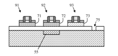
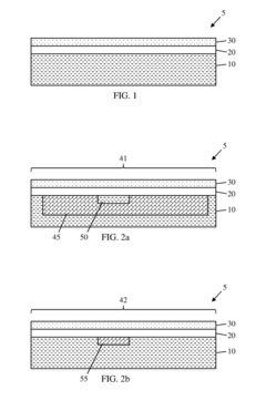
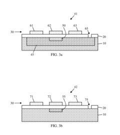
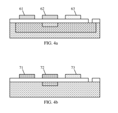
Fully depleted silicon-on-insulator device formation
PatentActiveUS20160372594A1
Innovation
- Forming gaps in the channel silicon germanium (SiGe) area to increase strain and mobility by epitaxially growing a doped SiGe layer on a buried oxide layer, with the gaps extending into the SiGe layer to a depth less than or equal to its thickness, and using techniques like sidewall image transfer or directed self-assembly to create striped structures that change the strain from biaxial to uniaxial, facilitating improved current flow and reducing source-drain resistance.
Fully-depleted silicon-on-insulator transistors
PatentActiveUS20180240815A1
Innovation
- The solution involves forming a semiconductor structure with multiple p-type and n-type FETs having different threshold voltages, where p-type FETs are over an n-well biased to VDD and n-type FETs are over a p-type substrate biased to ground, utilizing tailored doping and buried oxide layer thickness to achieve desired threshold voltages, consistent with standard bulk designs.
Power-Performance-Area Trade-offs Analysis
The power-performance-area (PPA) trade-off analysis between FinFET and FDSOI technologies reveals critical considerations for high-speed application designs. FinFET technology demonstrates superior performance characteristics at high operating voltages, with drive currents typically 15-20% higher than equivalent FDSOI implementations. This performance advantage makes FinFET particularly suitable for high-frequency operations exceeding 3GHz, where computational throughput is the primary concern.
However, FDSOI exhibits remarkable power efficiency advantages, especially at lower operating voltages. Measurements across comparable test chips show that FDSOI can achieve 20-30% lower dynamic power consumption at equivalent performance levels below 2.5GHz. The back-biasing capability unique to FDSOI provides an additional power management dimension, allowing for up to 40% power reduction in low-power modes while maintaining state retention.
From an area perspective, FinFET structures require more complex manufacturing processes with multiple fins and intricate 3D geometries. This complexity translates to approximately 10-15% larger cell areas compared to FDSOI at equivalent technology nodes. FDSOI's planar structure offers more straightforward design rules and potentially higher integration density for certain circuit blocks.
The trade-off analysis becomes particularly nuanced when considering specific application requirements. For high-performance computing applications requiring maximum clock speeds, FinFET's superior drive strength and lower variability at advanced nodes (7nm and below) generally outweigh its area disadvantages. Conversely, for mobile and IoT applications with stringent power budgets, FDSOI's excellent low-voltage performance and power management capabilities present compelling advantages despite potential performance limitations.
Temperature sensitivity further complicates the comparison, with FDSOI showing better performance retention at elevated temperatures due to reduced self-heating effects. Thermal measurements indicate that FinFET devices can experience 15-20% greater performance degradation at junction temperatures above 85°C compared to equivalent FDSOI implementations.
Recent benchmark studies across various high-speed circuit blocks (including SRAM, high-speed SerDes, and arithmetic units) demonstrate that the optimal technology choice depends heavily on the specific operating conditions and design constraints. FinFET maintains dominance in absolute performance metrics, while FDSOI offers superior energy efficiency metrics (MIPS/mW) when operating at moderate frequencies with aggressive voltage scaling.
Manufacturing Complexity and Cost Considerations
Manufacturing complexity and cost considerations represent critical factors in the semiconductor industry's adoption of advanced transistor architectures. FinFET technology, while offering superior performance characteristics, presents significant manufacturing challenges. The three-dimensional fin structure requires precise etching processes with extremely tight tolerances, necessitating advanced lithography techniques such as multi-patterning or EUV (Extreme Ultraviolet) lithography. These sophisticated manufacturing requirements translate directly to higher capital expenditure for fabrication facilities and increased production costs per wafer.
The complex geometry of FinFETs also results in lower manufacturing yields during early production phases, further increasing effective costs. Additionally, the intricate fin structure demands more mask layers and processing steps compared to planar technologies, extending production cycle times and reducing fab throughput. These factors collectively contribute to a higher cost structure that must be justified by performance advantages.
In contrast, FDSOI (Fully Depleted Silicon On Insulator) maintains a relatively simpler planar structure that aligns more closely with traditional CMOS manufacturing processes. The fabrication process requires fewer critical lithography steps and mask layers, resulting in reduced manufacturing complexity. The ultra-thin silicon layer in FDSOI can be produced with established SOI wafer manufacturing techniques, though the ultra-thin body requirements still present precision challenges.
FDSOI's manufacturing advantages translate to approximately 10-15% lower production costs compared to equivalent FinFET nodes. Furthermore, FDSOI fabrication facilities can often be established through upgrades to existing fabs rather than complete rebuilds, representing significant capital savings for semiconductor companies with legacy manufacturing infrastructure.
From a scaling perspective, FinFET demonstrates better dimensional scaling potential for sub-10nm nodes, though with escalating cost and complexity. FDSOI faces greater challenges at extremely advanced nodes but maintains cost advantages at 22nm and 14nm nodes where many high-speed applications currently operate.
The economic implications extend beyond direct manufacturing costs. FinFET's higher development costs and longer time-to-market can impact overall product economics, particularly for applications with moderate volume production where amortization of development costs becomes challenging. FDSOI offers a more favorable economic profile for mid-range performance applications where absolute cutting-edge performance is not required.
Unlock deeper insights with Patsnap Eureka Quick Research — get a full tech report to explore trends and direct your research. Try now!
Generate Your Research Report Instantly with AI Agent
Supercharge your innovation with Patsnap Eureka AI Agent Platform!