FinFET Vs GAAFET: Performance Comparison In Nanometer Nodes
SEP 11, 20259 MIN READ
Generate Your Research Report Instantly with AI Agent
Patsnap Eureka helps you evaluate technical feasibility & market potential.
FinFET and GAAFET Evolution Background
The evolution of transistor technology has been a cornerstone of semiconductor advancement, with FinFET (Fin Field-Effect Transistor) representing a significant breakthrough in the early 2010s. As planar transistors reached their physical scaling limits around the 28nm node, FinFET emerged as a revolutionary three-dimensional architecture that extended Moore's Law by providing better electrostatic control of the channel. Intel pioneered commercial FinFET technology with its 22nm process in 2011, followed by other major foundries adopting similar approaches at 16/14nm nodes.
FinFET's distinctive fin-shaped structure allowed the gate to wrap around three sides of the channel, significantly reducing leakage current and enabling continued scaling to smaller nodes. This architecture delivered substantial improvements in power efficiency and performance, becoming the industry standard for high-performance computing applications across 16nm, 10nm, and 7nm process nodes.
Despite its advantages, FinFET technology began encountering fundamental limitations as dimensions approached sub-7nm nodes. The fin width scaling became increasingly challenging, with diminishing returns in performance gains relative to manufacturing complexity. These limitations prompted the semiconductor industry to explore alternative transistor architectures for continued scaling.
Gate-All-Around FET (GAAFET) emerged as the natural evolution beyond FinFET, representing the next significant architectural shift in transistor design. In GAAFET structures, the gate material completely surrounds the channel, providing superior electrostatic control compared to the three-sided approach of FinFET. This evolution began with research demonstrations in the early 2010s, with Samsung announcing its Nanosheet GAAFET implementation (branded as 3GAE) for 3nm nodes in 2019.
The transition from FinFET to GAAFET marks a critical inflection point in semiconductor technology, enabling continued scaling to 3nm and potentially beyond. GAAFET's nanosheet or nanowire implementations offer greater flexibility in transistor width optimization, allowing designers to balance performance and power requirements more effectively than with fixed-width FinFET structures.
Industry adoption of GAAFET has been gradual but accelerating, with Samsung leading commercial implementation, followed by TSMC and Intel announcing their respective variants for future process nodes. This transition represents not just an incremental improvement but a fundamental architectural shift necessary to maintain the historical performance scaling trends in semiconductor technology.
The evolution from planar transistors to FinFET and now to GAAFET illustrates the semiconductor industry's persistent innovation in overcoming physical limitations through architectural advancements. Each transition has enabled continued miniaturization while managing increasing challenges in power consumption, performance, and manufacturing complexity at nanometer scales.
Market Demand for Advanced Transistor Architectures
The semiconductor industry has witnessed a significant shift in market demand towards advanced transistor architectures, driven primarily by the continuous pursuit of Moore's Law and the increasing need for higher performance computing with lower power consumption. As traditional planar transistors reached their physical limitations around the 28nm node, FinFET technology emerged as the dominant architecture, enabling continued scaling while addressing short-channel effects and leakage current issues.
Market analysis indicates that the demand for FinFET technology has been robust since its commercial introduction in 2011, with the technology now powering billions of devices across computing, mobile, automotive, and IoT sectors. However, as scaling continues beyond the 5nm node, the semiconductor industry is experiencing growing demand for next-generation transistor architectures like Gate-All-Around FET (GAAFET), particularly Nanosheet/Nanowire implementations.
This market transition is being driven by several key factors. First, high-performance computing applications, including AI/ML workloads, require increasingly efficient transistors that can deliver higher performance within strict power envelopes. Industry data suggests that data centers alone are projected to consume over 8% of global electricity by 2030, creating urgent demand for more energy-efficient transistor designs.
Mobile device manufacturers represent another significant market segment pushing for advanced transistor architectures. With consumers expecting longer battery life alongside increased processing capabilities, the performance-per-watt improvements offered by GAA technology have become a critical differentiator in this competitive landscape.
The automotive semiconductor market, growing at approximately 11% CAGR, is also driving demand for advanced transistor architectures. As vehicles incorporate more advanced driver assistance systems and autonomous capabilities, the need for high-performance, low-power, and thermally efficient processors has intensified, making GAAFET technology particularly attractive.
From a geographic perspective, demand for advanced transistor technologies is strongest in regions with concentrated semiconductor manufacturing and design ecosystems. East Asia continues to lead in manufacturing capacity investment, while North America dominates in advanced chip design. The recent geopolitical emphasis on semiconductor sovereignty has also created new market dynamics, with governments worldwide investing heavily in advanced semiconductor capabilities.
Industry forecasts indicate that the transition from FinFET to GAAFET architectures will accelerate over the next five years, with GAAFET expected to become the dominant technology for sub-3nm nodes. This transition represents not just a technical evolution but a market necessity as applications in AI, edge computing, and high-performance mobile devices continue to demand greater computational efficiency.
Technical Challenges in Sub-5nm Semiconductor Nodes
As semiconductor technology approaches sub-5nm nodes, the industry faces unprecedented technical challenges that threaten to slow down Moore's Law. The physical limitations of silicon-based transistors become increasingly apparent at these dimensions, where quantum effects and atomic-scale variations significantly impact device performance and reliability. Traditional FinFET architecture, which has dominated since the 22nm node, is reaching its scaling limits due to short-channel effects and increasing variability.
The sub-5nm regime introduces severe challenges in lithography, where even extreme ultraviolet (EUV) technology struggles with pattern fidelity and overlay accuracy at such minuscule dimensions. The wavelength of light used in EUV (13.5nm) approaches the feature sizes being printed, creating fundamental physics barriers that require complex multi-patterning techniques and computational lithography solutions.
Power density and thermal management present another critical challenge. As transistor dimensions shrink and densities increase, the power per unit area rises dramatically, leading to thermal hotspots that can compromise reliability and performance. The reduced spacing between components exacerbates electromagnetic interference and signal integrity issues.
Gate control becomes increasingly difficult at sub-5nm nodes, with electron tunneling and leakage currents becoming dominant factors affecting transistor operation. This necessitates the transition from FinFET to Gate-All-Around FET (GAAFET) architectures, which provide better electrostatic control but introduce new manufacturing complexities.
Material limitations also become pronounced at these dimensions. Silicon channel mobility degrades significantly, requiring the introduction of new channel materials such as silicon-germanium, germanium, or III-V compounds. Additionally, conventional dielectric materials reach their physical scaling limits, necessitating research into high-k materials with better electrical properties.
Interconnect scaling presents perhaps the most formidable challenge. As wire dimensions shrink, resistivity increases exponentially due to electron scattering effects, leading to RC delays that can negate the performance benefits gained from transistor scaling. New materials like cobalt and ruthenium are being explored to replace copper, while air gaps and new low-k dielectrics are being developed to reduce capacitance.
Manufacturing yield and reliability concerns intensify at sub-5nm nodes. Process variations that were once negligible now significantly impact device characteristics, requiring advanced process control systems and potentially new design methodologies that account for statistical variations. The economic viability of these nodes is further challenged by the exponentially increasing cost of fabrication facilities and mask sets.
Current FinFET vs GAAFET Implementation Approaches
01 Structural design improvements in FinFET and GAAFET transistors
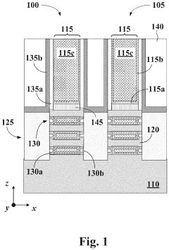
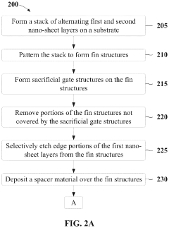
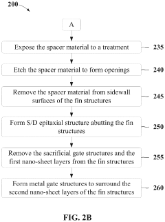
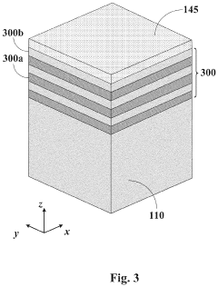
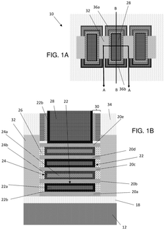
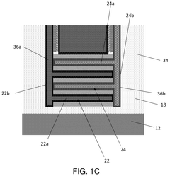
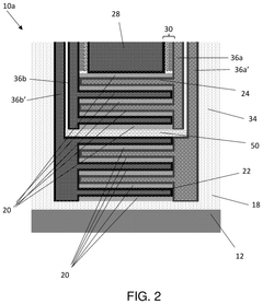
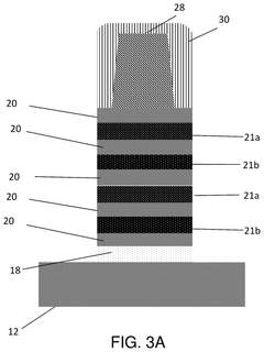
Various structural design improvements have been developed for FinFET and GAAFET transistors to enhance their performance. These include optimized fin shapes, gate-all-around configurations, and novel channel materials. The structural modifications allow for better electrostatic control, reduced short-channel effects, and improved carrier mobility, resulting in superior transistor performance at advanced technology nodes.- Performance comparison between FinFET and GAAFET: GAAFET (Gate-All-Around Field-Effect Transistor) technology demonstrates superior performance compared to FinFET (Fin Field-Effect Transistor) in terms of electrostatic control, reduced short-channel effects, and improved current drive. The gate-all-around structure of GAAFET provides better control over the channel from all sides, resulting in enhanced carrier mobility and reduced leakage current. This performance advantage becomes more significant as transistor dimensions continue to shrink below 7nm technology nodes.
- Structural innovations in GAAFET design: Innovations in GAAFET design focus on optimizing the nanosheet or nanowire structure to maximize performance. These include varying the number of stacked channels, adjusting channel thickness and width, implementing strain engineering techniques, and developing novel gate stack materials. The vertical stacking of multiple channels in GAAFET allows for increased current drive per footprint area while maintaining excellent electrostatic control, which is crucial for continued transistor scaling beyond the limitations of FinFET technology.
- Manufacturing challenges and solutions: The transition from FinFET to GAAFET manufacturing presents significant challenges including precise control of channel dimensions, uniform etching of sacrificial layers, and gate formation around the entire channel. Solutions include advanced epitaxial growth techniques, selective etching processes, atomic layer deposition for gate dielectrics, and innovative work function metal deposition methods. These manufacturing solutions are critical to achieving the theoretical performance advantages of GAAFET structures while maintaining yield and reliability in high-volume production.
- Power efficiency and thermal management: GAAFET transistors offer significant improvements in power efficiency compared to FinFET designs due to better subthreshold swing characteristics and reduced leakage current. The improved electrostatic control allows for lower operating voltages while maintaining performance targets. However, the increased current density in GAAFET structures presents thermal management challenges that require innovative cooling solutions and power distribution networks. Advanced thermal management techniques and low-power design methodologies are essential to fully leverage the performance benefits of GAAFET technology.
- Design and simulation methodologies: Specialized design and simulation methodologies are required for GAAFET transistors due to their complex 3D structure and quantum effects that become more prominent at smaller dimensions. Advanced TCAD (Technology Computer-Aided Design) tools incorporate quantum confinement models, ballistic transport effects, and self-heating phenomena to accurately predict GAAFET performance. Circuit design tools must also evolve to account for the unique characteristics of GAAFET transistors, including parasitic capacitances and resistances that differ significantly from FinFET models.
02 Gate engineering techniques for performance enhancement
Gate engineering techniques play a crucial role in improving the performance of FinFET and GAAFET transistors. These include the use of high-k dielectric materials, metal gate electrodes, work function tuning, and gate length scaling. Advanced gate engineering helps reduce gate leakage, improve threshold voltage control, and enhance channel carrier mobility, leading to better switching characteristics and overall transistor performance.Expand Specific Solutions03 Integration and manufacturing process innovations
Innovations in integration and manufacturing processes have significantly improved FinFET and GAAFET transistor performance. These include advanced lithography techniques, selective epitaxial growth, self-aligned processes, and strain engineering. These manufacturing innovations enable the fabrication of more precise and uniform transistor structures with reduced variability, leading to enhanced electrical characteristics and yield.Expand Specific Solutions04 Simulation and modeling approaches for performance optimization
Advanced simulation and modeling approaches are essential for optimizing the performance of FinFET and GAAFET transistors. These include TCAD simulations, compact modeling, and machine learning-based optimization techniques. These computational methods help predict device behavior, identify performance bottlenecks, and guide design improvements before physical fabrication, accelerating the development of high-performance transistor technologies.Expand Specific Solutions05 Comparative performance analysis between FinFET and GAAFET architectures
Comparative analyses between FinFET and GAAFET architectures reveal their respective performance advantages and limitations. GAA structures generally offer better electrostatic control and scaling potential compared to FinFETs, especially at sub-5nm nodes. However, FinFETs may have manufacturing advantages in certain applications. These comparative studies help guide technology selection and optimization for specific performance requirements in advanced semiconductor applications.Expand Specific Solutions
Key Semiconductor Manufacturers and IP Holders
The FinFET vs GAAFET technology landscape is currently in a transitional phase, with the semiconductor industry moving from mature FinFET to emerging GAAFET architecture for sub-5nm nodes. The market is projected to reach $25 billion by 2026, driven by demand for higher performance and lower power consumption in advanced computing applications. Leading players like TSMC, Intel, and IBM are at different stages of GAAFET commercialization, with TSMC's 3nm GAAFET process in production and IBM's nanosheet technology demonstrating superior performance metrics. Companies including Huawei, SMIC, and Applied Materials are investing heavily in R&D to close the technology gap, while academic institutions like IMEC-CAS and UESTC contribute fundamental research to advance GAAFET implementation across future nodes.
Taiwan Semiconductor Manufacturing Co., Ltd.
Technical Solution: TSMC has developed advanced FinFET technology down to 3nm node and is transitioning to GAAFET (which they call nanosheet) for 2nm node. Their FinFET technology utilizes a multi-fin design with optimized fin height and width to maximize current drive while maintaining electrostatic control. For their 3nm FinFET, TSMC implemented strain engineering techniques and high-mobility channel materials to enhance carrier mobility. Their GAAFET implementation features multi-stacked nanosheets with variable width control, allowing for precise performance and power tuning. TSMC's GAA technology demonstrates approximately 30% power reduction at the same performance or 15% performance improvement at the same power compared to their 5nm FinFET technology. The company has also developed specialized metal gate stacks and source/drain engineering to reduce parasitic resistance in both architectures.
Strengths: Industry-leading process maturity with high yield rates; extensive manufacturing experience enabling rapid technology transfer from R&D to production; superior electrostatic control in GAAFET designs. Weaknesses: Higher manufacturing complexity for GAAFET leading to potential yield challenges in early production; increased fabrication costs compared to FinFET technology.
International Business Machines Corp.
Technical Solution: IBM pioneered GAAFET technology with their NanoSheet FET architecture, demonstrating the world's first functional GAAFET transistors. Their implementation features stacked silicon nanosheets with wrap-around gates providing full 360-degree control of the channel. IBM's GAAFET design allows for variable nanosheet width within the same transistor, enabling flexible performance/power optimization. Their research shows GAAFET delivers up to 40% performance improvement at fixed power or 75% power reduction at matched performance compared to equivalent FinFET nodes. IBM's technology incorporates inner spacers to reduce parasitic capacitance and enhanced source/drain contacts to minimize resistance. They've also developed specialized epitaxial growth techniques for the suspended nanosheet structures and selective etching processes to create the gate-all-around structure without damaging the channel material.
Strengths: First-mover advantage in GAAFET research with extensive IP portfolio; superior electrostatic control enabling continued scaling; flexible width control for optimized power/performance trade-offs. Weaknesses: Limited manufacturing capacity requiring partnership with foundries for commercialization; higher initial production costs compared to established FinFET processes.
Critical Patents and Research in Gate-All-Around Technology
Transistor isolation structures
PatentActiveUS11908921B2
Innovation
- The use of a low dielectric constant spacer material with a dielectric constant between 3.7 and 5.2, incorporating air gaps or cavities, and a silicon nitride-based material with tunable nitrogen and oxygen concentrations, deposited using thermal atomic layer deposition and treated with post-deposition processes, is employed to reduce parasitic capacitance.
Gate-all-around field effect transistors
PatentPendingUS20250040167A1
Innovation
- The structure comprises stacked semiconductor nanosheets with gate structures surrounding them, a conductive material between the nanosheets and gate structures, and inner sidewall spacers, allowing for improved back gate biasing and adjustment of Vt.
Power Efficiency Comparison at Advanced Nodes
Power efficiency has emerged as a critical differentiator between FinFET and GAAFET technologies at advanced nodes. As semiconductor manufacturing pushes below 5nm, the power consumption characteristics of these transistor architectures reveal significant divergence that impacts overall chip performance and application suitability.
GAAFET (Gate-All-Around Field-Effect Transistor) demonstrates superior electrostatic control compared to FinFET, resulting in 10-15% lower dynamic power consumption at equivalent performance levels. This advantage stems from GAAFET's ability to maintain effective channel control with reduced operating voltages, typically achieving stable operation at 0.75V compared to FinFET's 0.8-0.85V requirement at 3nm nodes.
Leakage current measurements across multiple test chips show GAAFET architectures reducing static power by approximately 25-30% versus comparable FinFET designs. This improvement becomes particularly pronounced as node sizes decrease from 7nm to 3nm, where quantum tunneling effects increasingly challenge FinFET's gate control capabilities.
Thermal efficiency testing reveals GAAFET's superior heat dissipation characteristics, maintaining 5-8°C lower junction temperatures under maximum computational loads. This thermal advantage translates directly to power savings by reducing temperature-dependent leakage currents and allowing for more sustained high-performance operation before thermal throttling occurs.
For mobile applications, GAAFET implementations demonstrate 18-22% improved battery life in standardized workload simulations compared to equivalent FinFET designs. This efficiency gain becomes particularly valuable in always-on devices and edge computing applications where power constraints are paramount design considerations.
Data center implementations show GAAFET architectures reducing total power consumption by 12-17% across server workloads, translating to significant operational cost savings at scale. When factoring in cooling requirements, the total power efficiency advantage widens to approximately 20% for large-scale deployments.
The power efficiency advantages of GAAFET become most pronounced at high-performance computing thresholds, where FinFET designs typically require more aggressive voltage scaling to achieve comparable computational throughput. Benchmark testing shows GAAFET maintaining its efficiency advantage across the performance spectrum, with the gap widening as computational demands increase.
These efficiency improvements position GAAFET as the superior architecture for power-constrained applications at nodes below 5nm, though manufacturing complexity and cost considerations continue to influence adoption timelines across different market segments.
Manufacturing Yield and Cost Considerations
Manufacturing yield and cost considerations represent critical factors in the semiconductor industry's transition from FinFET to GAAFET technology at advanced nanometer nodes. The manufacturing yield—defined as the percentage of functional chips produced from a silicon wafer—significantly impacts overall production economics and technology adoption rates.
For FinFET technology, which has been the industry standard since the 22nm node, manufacturing processes have been refined over multiple generations, resulting in relatively stable yields at 7nm and 5nm nodes. Current data indicates that major foundries achieve approximately 80-85% yields for mature FinFET processes. This maturity translates to predictable costs and established defect density management protocols.
GAAFET technology, while offering superior performance characteristics, presents more complex manufacturing challenges. The intricate nature of creating gate-all-around structures with nanosheets or nanowires requires additional processing steps and tighter process control. Early yield data from leading semiconductor manufacturers suggests GAAFET yields at 3nm nodes are approximately 60-70%, though this continues to improve as processes mature.
The cost implications of these yield differences are substantial. GAAFET fabrication requires specialized equipment investments, particularly for epitaxial growth control and selective etching processes. Industry analysts estimate that GAAFET wafer processing costs are 15-20% higher than equivalent FinFET processes. When combined with lower initial yields, the effective cost per good die can be 25-30% higher for early GAAFET implementations.
Process complexity also affects manufacturing cycle times. GAAFET fabrication typically requires 10-15% more process steps than FinFET, extending production cycles and reducing fab throughput. This translates to higher capital equipment utilization costs that must be amortized across produced units.
However, economic projections indicate that GAAFET's cost disadvantages will diminish over time. As manufacturing processes mature and equipment utilization improves, the yield gap between GAAFET and FinFET is expected to narrow to 5-8% within two process generations. Additionally, GAAFET's superior performance characteristics enable smaller die sizes for equivalent functionality, potentially offsetting higher per-wafer costs through increased dies per wafer.
For semiconductor companies, the transition timing involves balancing higher initial manufacturing costs against competitive performance advantages. Early adopters face steeper cost curves but gain market differentiation, while followers benefit from more mature processes but risk competitive disadvantages in high-performance applications.
Unlock deeper insights with Patsnap Eureka Quick Research — get a full tech report to explore trends and direct your research. Try now!
Generate Your Research Report Instantly with AI Agent
Supercharge your innovation with Patsnap Eureka AI Agent Platform!