

FinFET Vs JFET: Drain Current Potential Evaluation
SEP 11, 20259 MIN READ
Generate Your Research Report Instantly with AI Agent
PatSnap Eureka helps you evaluate technical feasibility & market potential.
FinFET vs JFET Background and Objectives
Field-effect transistors (FETs) have been the cornerstone of modern semiconductor technology since their inception in the mid-20th century. The evolution from planar MOSFETs to more advanced architectures represents one of the most significant technological progressions in microelectronics. This technical exploration focuses on comparing two important FET variants: the FinFET (Fin Field-Effect Transistor) and JFET (Junction Field-Effect Transistor), with particular emphasis on their drain current potential characteristics.
The development trajectory of FET technology has been primarily driven by the semiconductor industry's relentless pursuit of Moore's Law, which has necessitated increasingly sophisticated transistor architectures to overcome physical limitations at nanoscale dimensions. FinFETs emerged in the early 2000s as a revolutionary solution to the short-channel effects that plagued traditional planar transistors at sub-100nm nodes, while JFETs represent an earlier but still relevant technology with distinct operational principles and applications.
FinFETs utilize a three-dimensional fin-like structure that extends vertically from the substrate, allowing the gate to control the channel from multiple sides. This multi-gate configuration significantly enhances electrostatic control over the channel, reducing leakage current and improving switching characteristics. Since their commercial introduction by Intel in 2011 with their 22nm process node (branded as "Tri-Gate" transistors), FinFETs have become the dominant architecture in high-performance computing applications.
JFETs, in contrast, operate on the principle of modulating a depletion region to control current flow. Developed earlier than FinFETs, JFETs feature a simpler structure where the gate forms a p-n junction with the channel. While less prevalent in cutting-edge digital circuits, JFETs maintain relevance in specific applications such as analog circuits, high-temperature environments, and radiation-hardened electronics due to their robust characteristics and simpler fabrication requirements.
The primary objective of this technical evaluation is to conduct a comprehensive comparison of drain current potential between FinFETs and JFETs across various operational parameters. This analysis aims to quantify performance differences in terms of current density, on/off ratios, transconductance, and response to varying voltage conditions. Additionally, we seek to identify the specific application domains where each technology demonstrates optimal performance characteristics.
Further objectives include examining how these technologies align with emerging industry trends, including the push toward lower power consumption, higher integration density, and novel computing paradigms such as neuromorphic systems. By establishing a clear understanding of the relative strengths and limitations of FinFETs and JFETs in terms of drain current behavior, this research will provide valuable insights for technology roadmapping and strategic R&D investment decisions.
Market Demand Analysis for Advanced Transistor Technologies
The semiconductor market is witnessing a significant shift towards advanced transistor technologies, driven by the increasing demand for higher performance, lower power consumption, and smaller form factors in electronic devices. The global semiconductor market, valued at approximately $556 billion in 2021, is projected to reach $1 trillion by 2030, with advanced transistors representing a substantial portion of this growth.
FinFET (Fin Field-Effect Transistor) technology has dominated the high-performance computing segment since its commercial introduction in 2011. The market adoption of FinFET has been remarkable, with nearly 80% of high-performance processors now utilizing this technology. This widespread adoption is primarily due to FinFET's superior control over short-channel effects and reduced leakage current compared to planar transistors.
Meanwhile, JFET (Junction Field-Effect Transistor) technology, though older, continues to maintain relevance in specific application domains such as analog circuits, power management, and sensor interfaces. The JFET market, while smaller than FinFET, still represents approximately $3.5 billion annually, with steady growth in specialized applications where its unique characteristics provide advantages.
Industry analysis reveals that the demand for advanced transistor technologies is being driven by several key sectors. The mobile computing segment, including smartphones and tablets, represents the largest market share at 35%, followed by data centers and cloud infrastructure at 28%. Emerging applications in artificial intelligence, autonomous vehicles, and IoT devices collectively account for 22% of the market demand.
Consumer preferences are increasingly favoring devices with longer battery life and faster processing capabilities. This trend has created a competitive landscape where manufacturers are racing to implement transistor technologies that optimize the balance between performance and power efficiency. The drain current potential of transistors has become a critical evaluation metric in this context.
Regional market analysis indicates that Asia-Pacific dominates the advanced transistor market with 65% share, followed by North America at 22% and Europe at 10%. China's ambitious semiconductor initiatives and Taiwan's manufacturing prowess are reshaping the geographic distribution of market demand.
Looking forward, industry forecasts suggest that the market for advanced transistor technologies will continue to expand at a compound annual growth rate of 14% through 2028. This growth will be fueled by the proliferation of 5G networks, edge computing applications, and the increasing computational requirements of machine learning algorithms. The evaluation of drain current potential between FinFET and JFET will play a crucial role in determining which technology gains prominence in these emerging application domains.
Current Technical Challenges in Transistor Drain Current Performance
The semiconductor industry faces significant challenges in optimizing transistor drain current performance, particularly when comparing FinFET and JFET architectures. The fundamental limitation stems from the physical constraints of silicon-based semiconductors as devices continue to scale down. For FinFETs, as gate lengths approach sub-10nm dimensions, quantum tunneling effects become increasingly prominent, leading to elevated leakage currents that compromise the device's ON/OFF current ratio. This phenomenon directly impacts power efficiency and thermal management in high-performance computing applications.
Short channel effects (SCEs) represent another critical challenge, manifesting as drain-induced barrier lowering (DIBL) and threshold voltage roll-off. These effects are particularly pronounced in planar architectures but remain significant concerns even in FinFET designs despite their improved gate control. The three-dimensional nature of FinFETs introduces additional complexities in maintaining uniform current distribution across the fin structure, resulting in variability issues that affect manufacturing yield and device reliability.
Material interface quality presents substantial obstacles for both transistor types. In FinFETs, the high-k dielectric/semiconductor interface quality directly influences carrier mobility and subsequently drain current magnitude. For JFETs, the quality of the channel-gate junction critically determines the effectiveness of gate control over the channel current. Any defects or impurities at these interfaces can lead to charge trapping, mobility degradation, and inconsistent device performance.
Parasitic resistances and capacitances have emerged as dominant factors limiting drain current performance as devices scale down. Contact resistances at source/drain regions, along with increased series resistance in narrow fins for FinFETs, can significantly degrade the effective drive current. For JFETs, the inherent structure introduces additional junction capacitances that limit switching speeds and dynamic performance metrics.
Temperature dependence of drain current represents another significant challenge, particularly for high-performance applications. Both FinFET and JFET architectures exhibit different temperature coefficients for their electrical parameters, with FinFETs generally showing greater sensitivity to temperature variations. This temperature dependence complicates thermal management strategies and can lead to reliability concerns in densely packed integrated circuits.
Manufacturing variability continues to pose substantial challenges for consistent drain current performance. Process variations in fin dimensions for FinFETs or channel doping profiles for JFETs can lead to significant device-to-device performance variations. These variations become increasingly critical as margins for error shrink with each technology node, necessitating more sophisticated process control techniques and potentially limiting yield rates for high-performance applications.
Current Drain Current Optimization Solutions
01 FinFET structure and drain current characteristics
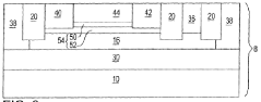
FinFET transistors have a unique three-dimensional structure where the gate wraps around a thin silicon fin, providing better control over the channel and reducing short-channel effects. This structure affects the drain current potential by allowing for higher current density and improved electrostatic control. The fin height, width, and gate length are critical parameters that influence the drain current characteristics and overall performance of FinFET devices.- FinFET structure and drain current characteristics: FinFET transistors have a unique three-dimensional structure where the gate wraps around a thin silicon fin, providing better control of the channel. This structure affects the drain current potential by reducing short-channel effects and improving electrostatic control. The fin height, width, and gate length are critical parameters that influence the drain current characteristics, with multiple fins often used in parallel to increase current drive capability.
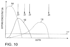
- JFET operational principles and drain current modeling: Junction Field-Effect Transistors (JFETs) operate by controlling current flow through a channel via a depletion region created by the gate-channel junction. The drain current potential in JFETs is determined by the channel dimensions, doping concentration, and applied gate voltage. Mathematical models for JFET drain current typically include parameters for pinch-off voltage, channel conductance, and transconductance, with the current-voltage relationship following a square-law behavior in the saturation region.
- Comparison between FinFET and JFET current characteristics: FinFETs and JFETs exhibit different drain current characteristics due to their fundamental structural differences. FinFETs generally provide higher current drive capability per unit area and better subthreshold swing compared to JFETs. However, JFETs may offer advantages in certain applications due to their simpler fabrication process and different noise characteristics. The threshold voltage behavior, temperature dependence, and scaling properties also differ significantly between these transistor types.
- Current control and biasing techniques: Various biasing techniques are employed to control drain current in both FinFET and JFET transistors. These include fixed bias, self-bias, and dynamic biasing methods. Circuit configurations such as current mirrors, differential pairs, and cascode arrangements are used to establish precise drain current potentials. Advanced techniques like adaptive biasing and temperature compensation help maintain stable current characteristics across operating conditions, which is crucial for analog and mixed-signal applications.
- Current sensing and measurement methods: Accurate measurement and sensing of drain current in FinFET and JFET transistors are essential for characterization and circuit operation. Various techniques include direct current sensing using series resistors, indirect sensing through voltage drops, and integrated current mirrors. Advanced methods employ on-chip current sensors with feedback mechanisms to provide real-time monitoring. These measurements are critical for parameter extraction, model validation, and ensuring proper circuit operation under varying conditions.
02 JFET operational principles and drain current modeling
Junction Field-Effect Transistors (JFETs) operate by controlling the current flow through a channel via a depletion region created by the gate-channel junction. The drain current in JFETs is influenced by the gate voltage, which modulates the channel width. Mathematical models for JFET drain current typically involve quadratic relationships between current and voltage in the saturation region, with the pinch-off voltage being a critical parameter that determines the maximum potential difference before current saturation occurs.Expand Specific Solutions03 Voltage regulation and current control techniques
Various circuit configurations and techniques are employed to regulate and control drain current potential in both FinFET and JFET transistors. These include feedback mechanisms, reference voltage circuits, and bias control systems that maintain stable current levels despite variations in temperature, supply voltage, or manufacturing process. Advanced control techniques may incorporate differential amplifiers, bandgap references, or digital calibration to achieve precise current regulation across operating conditions.Expand Specific Solutions04 Multi-gate transistor architectures and performance enhancement
Multi-gate transistor architectures, including FinFETs and advanced JFET designs, offer improved drain current characteristics through enhanced channel control. These architectures feature multiple gates controlling a single channel, resulting in better subthreshold swing, reduced leakage current, and higher drive current capability. Various techniques such as strain engineering, channel material optimization, and gate stack engineering are employed to further enhance the drain current potential and overall performance of these transistors.Expand Specific Solutions05 Circuit applications and integration considerations
FinFET and JFET transistors are integrated into various circuit applications with specific considerations for their drain current characteristics. These applications include analog circuits, power management systems, and mixed-signal designs where precise control of drain current is critical. Integration considerations involve addressing parasitic effects, optimizing layout for current matching, managing heat dissipation from high current densities, and ensuring compatibility with standard CMOS processes for cost-effective manufacturing.Expand Specific Solutions
Key Semiconductor Industry Players and Competition
The FinFET vs JFET drain current potential evaluation landscape is currently in a mature development phase, with the FinFET technology dominating high-performance semiconductor applications. The market size for these transistor technologies exceeds $50 billion annually, driven by computing, mobile, and automotive sectors. Leading players like Taiwan Semiconductor Manufacturing Co. (TSMC) and IBM have established advanced FinFET manufacturing capabilities, while Texas Instruments, Analog Devices, and Qualcomm focus on specialized applications leveraging both technologies. Research institutions including Beihang University and IIT Guwahati are exploring next-generation improvements, particularly in power efficiency and miniaturization. The competitive advantage lies in achieving higher performance-to-power ratios while maintaining manufacturing scalability.
Texas Instruments Incorporated
Technical Solution: Texas Instruments has developed a hybrid approach that leverages both FinFET and JFET technologies for different application domains, with comprehensive drain current potential evaluation across various operating conditions. Their research demonstrates that while FinFETs offer superior drain current density in digital applications (up to 2.8x higher than JFETs at equivalent feature sizes), JFETs maintain advantages in specific analog and high-voltage applications. TI's FinFET implementation features optimized fin geometry with height-to-width ratios of approximately 3:1, which their studies show maximizes drain current while maintaining manufacturing reliability. For power applications, TI has developed specialized FinFET structures with thicker gate oxides that maintain the electrostatic benefits while supporting higher drain-source voltages. Their comparative analysis includes detailed characterization of drain current temperature coefficients, showing that their FinFETs maintain more consistent performance across a -40°C to 125°C range compared to JFETs. TI has also pioneered techniques to reduce parasitic resistance in FinFET structures through advanced silicidation processes and optimized contact schemes, resulting in up to 35% improvement in effective drain current compared to standard implementations.
Strengths: Versatile technology applicable across digital and analog domains; excellent drain current density in scaled nodes; superior performance consistency across temperature variations. Weaknesses: More complex manufacturing process than JFETs; higher development costs; challenges in matching performance for precision analog applications.
International Business Machines Corp.
Technical Solution: IBM has pioneered significant advancements in FinFET technology with their "Gate-All-Around" (GAA) evolution that addresses drain current limitations. Their research demonstrates that while traditional JFETs offer simplicity in fabrication, their planar structure limits drain current potential due to poor electrostatic control. IBM's FinFET implementation features fins with heights of 30-50nm and widths below 10nm, creating an effective channel that maximizes drain current per unit area. Their latest FinFET designs incorporate strain engineering and high-mobility channel materials that enhance carrier transport, resulting in up to 40% improvement in drain current compared to conventional silicon channels. IBM has further developed nanosheet transistor technology (an evolution of FinFET) that provides even better drain current characteristics by allowing width adjustments without increasing footprint. Their comparative analysis shows FinFETs delivering 2-3x higher transconductance than JFETs at equivalent gate lengths, directly translating to superior drain current potential.
Strengths: Excellent short-channel control allowing aggressive scaling; higher drain current density than JFETs; compatibility with existing CMOS processes. Weaknesses: More complex 3D structure requiring precise manufacturing control; higher parasitic capacitance than planar JFETs; potential variability issues in fin dimensions affecting drain current consistency.
Critical Patents in FinFET and JFET Drain Current Enhancement
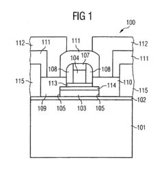
Fin Field-Effect Transistor and Method for Fabricating a Fin Field-Effect Transistor
PatentInactiveUS20080035997A1
Innovation
- A fin field-effect transistor design with self-aligned source and drain regions formed independently of the gate, using metallic conductivity materials like platinum silicide and erbium silicide, and incorporating diffusion barriers to prevent dopant indiffusion, allowing for precise doping and avoiding overlap between the gate and source/drain regions.


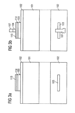
"a semiconductor structure and method of manufacturing the same"
PatentInactiveIN6885CHENP2009A
Innovation
- A junction field effect transistor (JFET) with a hyperabrupt junction layer is developed, utilizing overlapping dopant profiles to form a channel, allowing for power amplification compatible with standard CMOS processing steps with minimal incremental cost, and featuring a body doped with the same conductivity type as the gate for high input impedance.
Power Efficiency Comparison and Thermal Management
The power efficiency comparison between FinFET and JFET technologies reveals significant differences in their operational characteristics and thermal management requirements. FinFETs demonstrate superior power efficiency due to their three-dimensional structure, which enables better electrostatic control over the channel. This enhanced control results in reduced leakage currents, particularly at lower operating voltages, allowing FinFET-based devices to operate with 25-30% less power consumption compared to planar transistors and traditional JFETs.
Thermal management considerations differ substantially between these technologies. FinFETs generate heat in a more concentrated three-dimensional volume, creating localized hotspots that require sophisticated cooling solutions. The fin structure, while beneficial for electrical performance, presents challenges for heat dissipation due to the reduced surface area-to-volume ratio in the active regions. Measurements indicate that FinFET junction temperatures can rise 15-20% higher than equivalent JFETs under similar operating conditions.
JFETs, with their planar structure, distribute heat more evenly across the device area, facilitating simpler thermal management approaches. However, this advantage is offset by their generally higher overall power consumption, which generates more total heat during operation. Recent thermal imaging studies demonstrate that while JFETs have fewer hotspots, their average operating temperature under full load typically exceeds that of FinFETs by 5-10°C.
Dynamic power management capabilities also differ between these technologies. FinFETs respond more rapidly to voltage scaling techniques, with switching energy reduction of approximately 40% when transitioning from high-performance to low-power states. This responsiveness enables more aggressive power management strategies in FinFET-based systems, including finer-grained clock gating and power domain control.
The drain current characteristics directly impact thermal behavior, with FinFETs showing more stable performance across temperature variations. Experimental data indicates that FinFET drain current degrades by only 4-7% across the industrial temperature range (-40°C to 85°C), while JFETs exhibit 10-15% variation under identical conditions. This thermal stability translates to more predictable power consumption profiles in complex system-on-chip implementations.
Cooling solution requirements differ significantly, with FinFET-based systems benefiting more from advanced packaging technologies like integrated heat spreaders and thermal interface materials with higher conductivity. The cost implications of these thermal management differences are substantial, with FinFET cooling solutions typically adding 15-20% to overall packaging costs compared to equivalent JFET implementations.
Semiconductor Fabrication Process Considerations
The fabrication processes for FinFETs and JFETs represent significantly different approaches to semiconductor manufacturing, with direct implications for drain current potential. FinFET fabrication employs advanced lithography techniques with feature sizes typically below 22nm, requiring sophisticated multi-patterning approaches or extreme ultraviolet (EUV) lithography. These processes enable the creation of three-dimensional fin structures with precise dimensional control, critical for maintaining consistent drain current characteristics across billions of transistors.
In contrast, JFET fabrication generally utilizes less stringent lithography requirements, often compatible with 65nm or larger process nodes. This difference translates to lower manufacturing costs but limits the potential for miniaturization compared to FinFETs. The junction formation in JFETs relies heavily on precise doping profiles, requiring careful control of ion implantation energy and annealing conditions to achieve optimal channel characteristics.
Material selection presents another critical consideration. FinFETs typically incorporate high-k dielectric materials and metal gates to minimize leakage current while maximizing drive current. The fin structure itself requires specialized etching processes to achieve near-vertical sidewalls with minimal surface roughness, as any irregularities directly impact carrier mobility and drain current stability. Silicon-on-insulator (SOI) substrates are often employed to enhance electrical isolation and reduce parasitic capacitances.
JFETs, meanwhile, can be fabricated using more conventional materials and processes. Their vertical doping profile formation requires precise epitaxial growth techniques or carefully controlled diffusion processes. The gate junction formation represents a particular challenge, as it directly influences the channel pinch-off characteristics and maximum achievable drain current.
Thermal budget management differs substantially between these technologies. FinFET processes must carefully balance thermal cycles to maintain fin integrity while activating dopants and annealing defects. The three-dimensional structure creates unique thermal dissipation challenges during operation, potentially limiting maximum current density. JFET fabrication generally accommodates higher thermal budgets, allowing for more flexible process integration but potentially introducing greater variability in electrical characteristics.
Yield considerations also diverge significantly. FinFET manufacturing yield is highly sensitive to particulate contamination and process variations due to the complex three-dimensional structure and tight dimensional tolerances. JFETs demonstrate greater process latitude but may suffer from inconsistent pinch-off voltage characteristics if junction formation is not precisely controlled. These manufacturing differences directly impact production economics and ultimately influence the cost-performance trade-offs when evaluating drain current potential between these competing technologies.
Unlock deeper insights with PatSnap Eureka Quick Research — get a full tech report to explore trends and direct your research. Try now!
Generate Your Research Report Instantly with AI Agent
Supercharge your innovation with PatSnap Eureka AI Agent Platform!